 | –≠–ª–µ–∫—Ç—Ä–æ–Ω–Ω—ã–π –∫–æ–º–ø–æ–Ω–µ–Ω—Ç: EL2005 | –°–∫–∞—á–∞—Ç—å:  PDF PDF  ZIP ZIP |

EL2005EL2005C
January
1990
Rev
F
EL2005 EL2005C
High Accuracy Fast Buffer
Note All information contained in this data sheet has been carefully checked and is believed to be accurate as of the date of publication however this data sheet cannot be a ``controlled document'' Current revisions if any to these
specifications are maintained at the factory and are available upon your request We recommend checking the revision level before finalization of your design documentation Patent pending
CMS
2005DS
1989 Elantec Inc
Features
Low input current
50 pA
Low offset and drift
2 mV 25
mV C
High slew rate
1500 V
ms
Fast rise and fall time
2 5 ns
High input resistance
1000 G
X
Bandwidth
140 MHz
Pin compatible with ELH0033
MIL-STD-883 Revision C devices
manufactured in U S A
Advantages
No input loading
Input current independent of
input voltage
Eliminates offset adjustments
Drives cables directly
Ordering Information
Part No
Temp Range
Package Outline
EL2005CG
b
25 C to
a
85 C
TO-8
MDP0002
EL2005G
b
55 C to
a
125 C
TO-8
MDP0002
EL2005G 883B
b
55 C to
a
125 C
TO-8
MDP0002
Connection Diagram
2005 ≠ 1
Top View
Note Case is electrically isolated
General Description
The EL2005 is a high-speed
FET input buffer similar to
ELH0033 and EL2004 but with input specifications significant-
ly improved over the previous types The input stage employs a
cascode configuration to maintain constant input characteris-
tics over the full
g
10V input range The input looks like a 3 pF
capacitor to ground in almost all cases since the DC bias current
is constant with input voltage In sample and hold circuits this
results in an order of magnitude improvement in hold charac-
teristics Input offset voltage and offset voltage drift are also
improved a factor of two over previous types
These excellent DC characteristics are complemented by a wide
140 MHz bandwidth while the 1500 V
ms slew rate and excel-
lent phase linearity of the ELH0033 family are preserved allow-
ing direct plug-in replacement for upgraded performance (For
even faster operation see EL2004 )
Elantec facilities comply with MIL-I-45208A and are MIL-
STD-1772 certified
Elantec's Military devices comply with
MIL-STD-883B Revision C and are manufactured in our rigidly
controlled ultra-clean facilities in Milpitas California For ad-
ditional information on Elantec's Quality and Reliability Assur-
ance Policy and procedures request brochure QRA-1
Simplified Schematic
2005 ≠ 2
EL2005 EL2005C
High Accuracy Fast Buffer
Absolute Maximum Ratings
(T
A
e
25 C)
V
S
Supply Voltage (V
a b
V
b
)
40V
V
IN
Input Voltage
40V
P
D
Power Dissipation (See curves)
1 5W
I
OC
Continuous Output Current
g
100 mA
I
OP
Peak Output Current
g
250 mA
T
A
Operating Temperature Range
EL2005
b
55 C to
a
125 C
EL2005C
b
25 C to
a
85 C
T
J
Operating Junction Temperature
175 C
T
ST
Storage Temperature
b
65 C to
a
150 C
Lead Temperature
(Soldering 10 seconds)
300 C
Important Note
All parameters having Min Max specifications are guaranteed The Test Level column indicates the specific device testing actually
performed during production and Quality inspection Elantec performs most electrical tests using modern high-speed automatic test
equipment specifically the LTX77 Series system Unless otherwise noted all tests are pulsed tests therefore T
J
e
T
C
e
T
A
Test Level
Test Procedure
I
100% production tested and QA sample tested per QA test plan QCX0002
II
100% production tested at T
A
e
25 C and QA sample tested at T
A
e
25 C
T
MAX
and T
MIN
per QA test plan QCX0002
III
QA sample tested per QA test plan QCX0002
IV
Parameter is guaranteed (but not tested) by Design and Characterization Data
V
Parameter is typical value at T
A
e
25 C for information purposes only
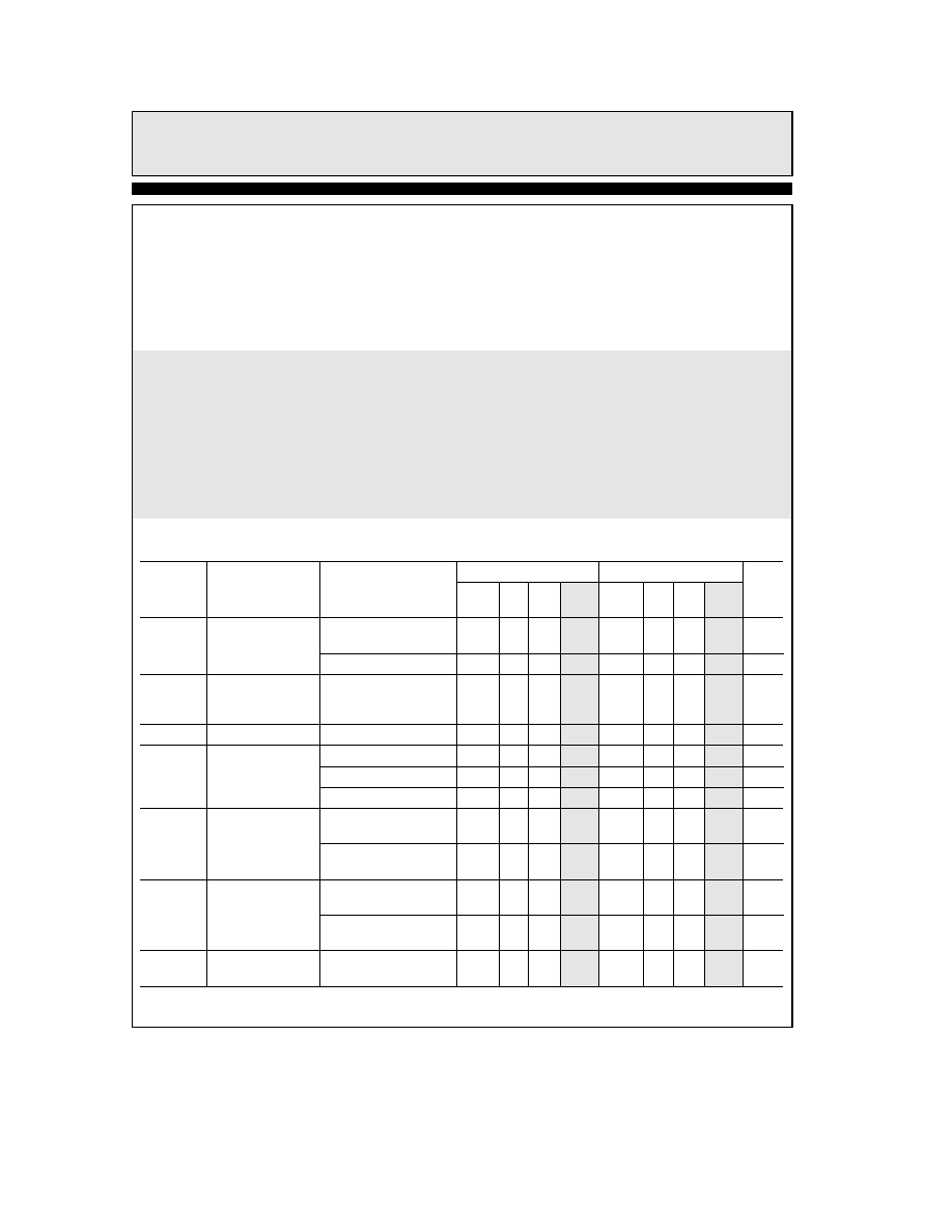
DC Electrical Characteristics
V
S
e
g
15V V
IN
e
0V T
MIN
s
T
A
s
T
MAX
Parameter
Description
Test Conditions
EL2005
EL2005C
Units
Min
Typ Max
Test
Min
Typ Max
Test
Level
Level
V
OS
Output Offset
R
S
s
100 k
X T
J
e
25 C
2
5
I
3
10
I
mV
Voltage
(Note 1)
R
S
s
100 k
X
10
I
15
III
mV
DV
OS
DT
Average Temperature
Coefficient of
R
S
e
100
X
25
V
25
V
mV C
Offset Voltage
PSRR
Supply Rejection
g
10V
s
V
S
s g
20V
65
75
I
60
75
II
dB
I
B
Input Bias Current
T
J
e
25 C (Notes 1 and 3)
2
50
I
5
100
I
pA
T
A
e
25 C (Notes 2 and 3)
50
500
IV
100
1000
IV
pA
T
J
e
T
A
e
T
MAX
2
5
I
0 5
5
III
nA
A
V
Voltage Gain
R
S
e
100
X R
L
e
1 k
X
0 97
0 98
1 0
I
0 96
0 98
1 0
II
V V
V
IN
e
g
10V
R
S
e
100
X R
L
e
100
X
0 88
0 95
0 98
I
0 88
0 95
0 99
II
V V
v
IN
e
g
10V
R
IN
Input Impedance
R
L
e
1 k
X
2
c
10
9
10
12
I
2
c
10
9
10
12
IV
X
b
10V
s
V
IN
s g
10V
T
J
e
25 C (Note 1)
10
10
10
12
I
10
10
10
12
I
X
R
L
e
1 k
X
R
O
Output
R
L
e
1 k
X
4
8
I
4
9
II
X
Impedance
V
IN
e
g
1V
2
TD
is
38in
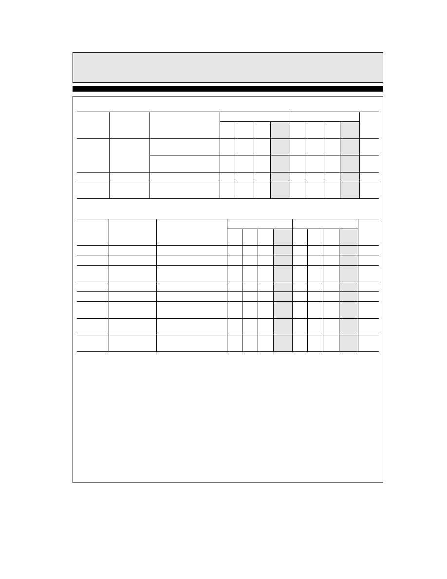
EL2005 EL2005C
High Accuracy Fast Buffer
DC Electrical Characteristics
V
S
e
g
15V V
IN
e
0V T
MIN
s
T
A
s
T
MAX
Contd
Parameter
Description
Test Conditions
EL2005
EL2005C
Units
Min
Typ
Max
Test
Min
Typ
Max
Test
Level
Level
V
O
Output Voltage
V
IN
e
g
14V
g
12 5
V
g
12 5
V
V
Swing
R
L
e
1 k
X
V
IN
e
g
10 5V R
L
e
100
X
g
9
g
9 8
I
g
9
g
9 8
I
V
T
A
e
25 C
I
S
Supply Current
V
IN
e
0 (Note 1)
19
22
I
19
24
II
mA
PD
Power
V
IN
e
0
570
660
I
570
720
II
mW
Consumption
AC Electrical Characteristics
T
C
e
25 C V
S
e
g
15V R
S
e
50
X R
L
e
1 k
X
Parameter
Description
Test Conditions
EL2005
EL2005C
Units
Min
Typ
Max
Test
Min
Typ
Max
Test
Level
Level
SR
Slew Rate
V
IN
e
g
10V V
OUT
e
g
5V
1000
1500
III
1000
1500
III
V
ms
BW
Bandwidth
V
IN
e
1 V
rms
140
V
140
V
MHz
w
NL
Phase
BW
e
1 MHz to 20 MHz
2
V
2
V
Degree
Non-Linearity
t
r
Rise Time
DV
IN
e
0 5V
2 5
V
2 5
V
ns
t
P
Propagation Delay
DV
IN
e
0 5V
1 0
V
1 0
V
ns
HD
Harmonic
f
l
1 kHz
k
0 1
V
k
0 1
V
%
Distortion
A
V
Voltage Gain
R
S
e
100
X V
IN
e
1 V
rms
0 97
0 99
1 0
I
0 96
0 99
1 0
II
V V
f
e
1 kHz
R
O
Output Impedance
V
IN
e
1 V
rms
4
8
I
4
9
II
X
f
e
1 kHz
Note 1 Specification is at 25 C junction temperature due to requirements of high-speed automatic testing Actual values at operating
temperatures will exceed the value at T
J
e
25 C When supply voltages are
g
15V no-load operating junction temperatures
may rise 40 C to 60 C above ambient and more under load conditions Accordingly V
OS
may change one to several mV and
I
B
will change significantly during warm-up Refer to I
B
vs Temperature graph for expected values
Note 2 Measured in still air seven minutes after application of power
Note 3 Input bias current is guaranteed over the input range of
b
10V
s
V
IN
s
a
10V
3
TD
is
17in
TD
is
25in
EL2005 EL2005C
High Accuracy Fast Buffer
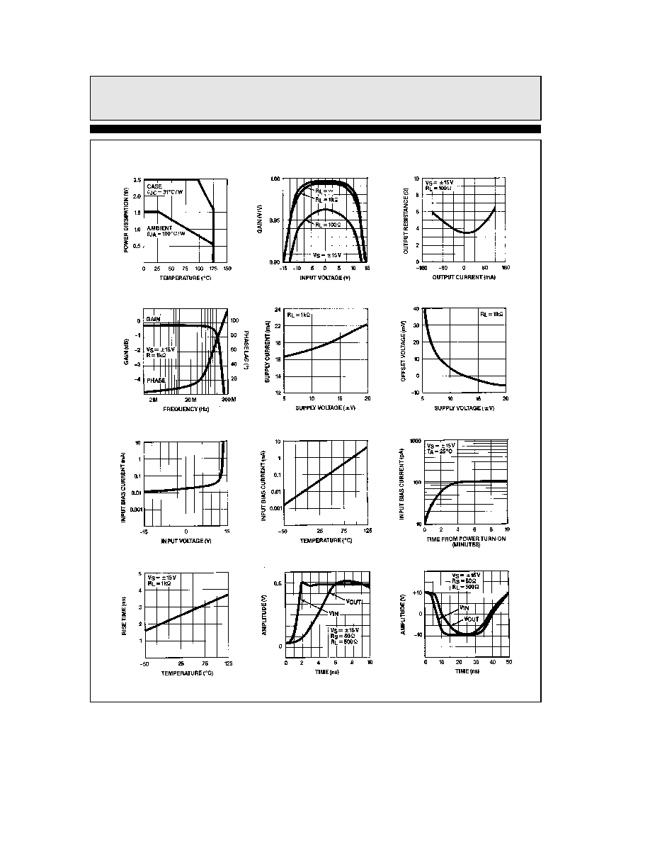
Typical Performance Curves
Dissipation
Maximum Power
Gain vs Input Voltage
Output Resistance vs
Output Current
Frequency Response
Supply Voltage
Supply Current vs
Offset Voltage vs
Supply Voltage
2005 ≠ 3
Input Voltage
Input Bias Current vs
Temperature
Input Bias Current vs
During Warm-up
Input Bias Current
Temperature
Rise Time vs
Small Signal Pulse
Response
Large Signal Pulse
Response
2005 ≠ 4
4
EL2005 EL2005C
High Accuracy Fast Buffer
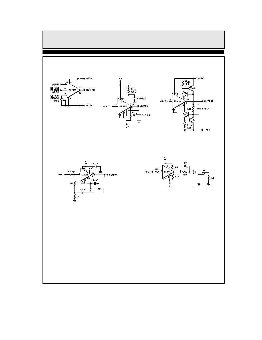
Typical Applications
Offset Zero Adjust
2005 ≠ 5
Using Resistor
Current Limiting
2005 ≠ 6
Current Limiting
Using Current Sources
2005 ≠ 7
Q1
e
Q2
e
2N2905
Q3
e
Q4
e
2N2219
High Input Impedance
AC Coupled Amplifier
2005 ≠ 8
Coaxial Cable Driver
Select C1 for optimum pulse response
2005 ≠ 9
5