 | –≠–ª–µ–∫—Ç—Ä–æ–Ω–Ω—ã–π –∫–æ–º–ø–æ–Ω–µ–Ω—Ç: EL2020CM | –°–∫–∞—á–∞—Ç—å:  PDF PDF  ZIP ZIP |
EL2020C
December
1995
Rev
G
EL2020C
50 MHz Current Feedback Amplifier
Note All information contained in this data sheet has been carefully checked and is believed to be accurate as of the date of publication however this data sheet cannot be a ``controlled document'' Current revisions if any to these
specifications are maintained at the factory and are available upon your request We recommend checking the revision level before finalization of your design documentation
1989 Elantec Inc
Features
Slew rate 500 V ms
g
33 mA output current
Drives
g
2 4V into 75
X
Differential phase
k
0 1
Differential gain
k
0 1%
V supply
g
5V to
g
18V
Output short circuit protected
Uses current mode feedback
1% settling time of 50 ns for 10V
step
Low cost
9 mA supply current
8-pin mini-dip
Applications
Video gain block
Residue amplifier
Radar systems
Current to voltage converter
Coax cable driver with
gain of 2
Ordering Information
Part No
Temp Range
Pkg
Outline
EL2020CN
b
40 C to a85 C P-DIP
MDP0031
EL2020CM
b
40 C to a85 C 20-Lead MDP0027
SOL
General Description
The EL2020 is a fast settling wide bandwidth amplifier opti-
mized for gains between
b
10 and
a
10 Built using the Elantec
monolithic Complementary Bipolar process this amplifier uses
current mode feedback to achieve more bandwidth at a given
gain then a conventional voltage feedback operational amplifi-
er
The EL2020 will drive two double terminated 75
X coax cables
to video levels with low distortion Since it is a closed loop de-
vice the EL2020 provides better gain accuracy and lower distor-
tion than an open loop buffer The device includes output short
circuit protection and input offset adjust capability
The bandwidth and slew rate of the EL2020 are relatively inde-
pendent of the closed loop gain taken The 50 MHz bandwidth
at unity gain only reduces to 30 MHz at a gain of 10 The
EL2020 may be used in most applications where a conventional
op amp is used with a big improvement in speed power prod-
uct
Elantec products and facilities comply with Elantec document
QRA-1 Processing-Monolithic Products
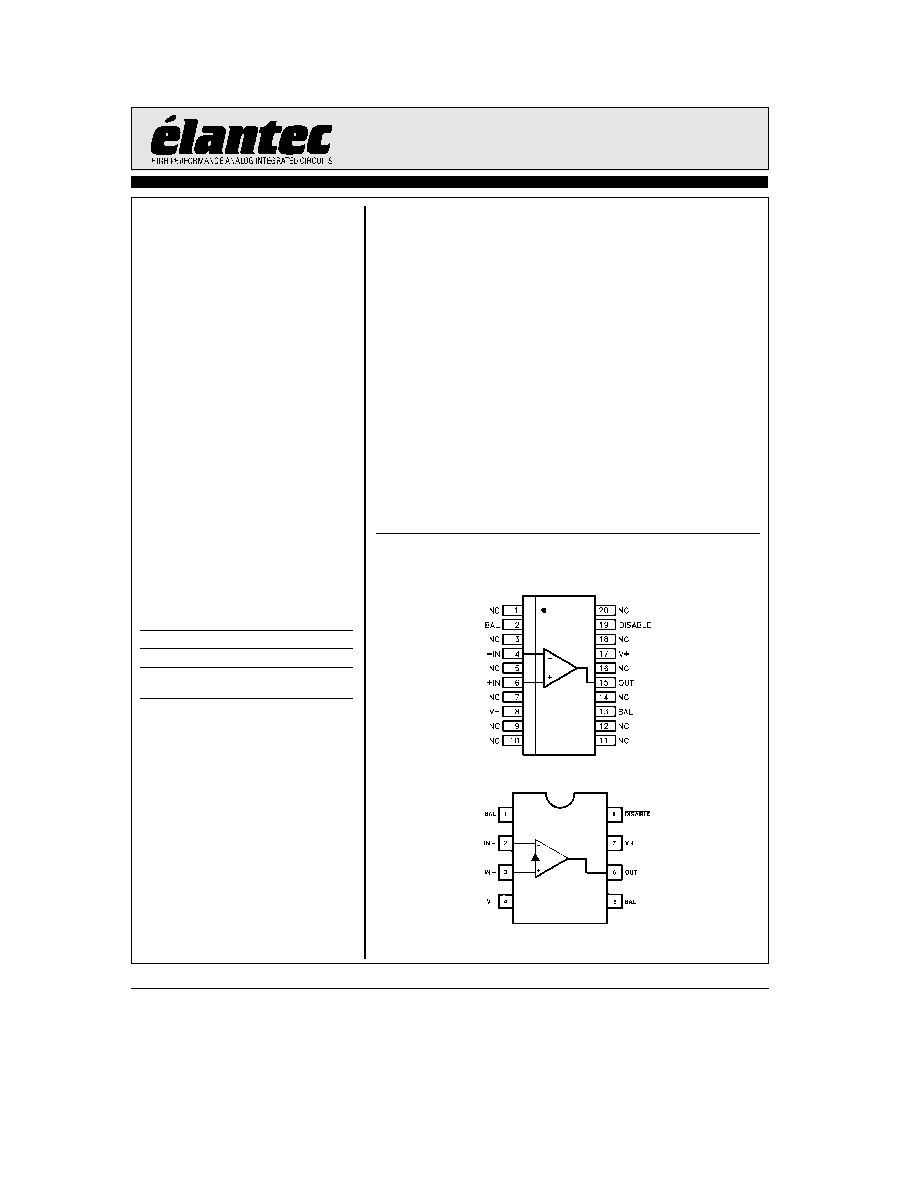
Connection Diagrams
SOL
2020 ≠ 2
DIP
2020 ≠ 1
Manufactured under U S Patent No 4 893 091

EL2020C
50 MHz Current Feedback Amplifier
Absolute Maximum Ratings
(25 C)
V
S
Supply Voltage
g
18V or 36V
V
IN
Input Voltage
g
15V or V
S
DV
IN
Differential Input Voltage
g
10V
I
IN
Input Current (Pins 2 or 3)
g
10 mA
I
INS
Input Current (Pins 1 5 or 8)
g
5 mA
P
D
Maximum Power Dissipation
(See Curves)
1 25W
I
OP
Peak Output Current
Short Circuit
Protected
Output Short Circuit Duration
(Note 2)
Continuous
T
A
Operating Temperature Range
b
40 C to
a
85 C
T
J
Operating Junction Temperature
Plastic Package SOL
150 C
T
ST
Storage Temperature
b
65 C to
a
150 C
Important Note
All parameters having Min Max specifications are guaranteed The Test Level column indicates the specific device testing actually
performed during production and Quality inspection Elantec performs most electrical tests using modern high-speed automatic test
equipment specifically the LTX77 Series system Unless otherwise noted all tests are pulsed tests therefore T
J
e
T
C
e
T
A
Test Level
Test Procedure
I
100% production tested and QA sample tested per QA test plan QCX0002
II
100% production tested at T
A
e
25 C and QA sample tested at T
A
e
25 C
T
MAX
and T
MIN
per QA test plan QCX0002
III
QA sample tested per QA test plan QCX0002
IV
Parameter is guaranteed (but not tested) by Design and Characterization Data
V
Parameter is typical value at T
A
e
25 C for information purposes only
Open Loop Characteristics
V
S
e
g
15V
Parameter
Description
Temp
Limits
Test Level
Units
Min
Typ
Max
V
OS
(Note 1)
Input Offset Voltage
25 C
b
10
3
a
10
I
mV
T
MIN
T
MAX
b
15
a
15
III
mV
DV
OS
DT
Offset Voltage Drift
b
30
V
mV C
CMRR (Note 3)
Common Mode Rejection Ratio
ALL
50
60
II
dB
PSRR (Note 4)
Power Supply Rejection Ratio
25 C
65
75
I
dB
T
MIN
T
MAX
60
III
dB
a
I
IN
Non-inverting Input Current
25 C T
MAX
b
15
5
a
15
II
mA
T
MIN
b
25
a
25
III
mA
a
R
IN
Non-Inverting Input Resistance
ALL
1
5
II
M
X
a
IPSR (Note 4)
Non-Inverting Input Current
25 C T
MAX
0 05
0 5
II
mA V
Power Supply Rejection
T
MIN
1 0
III
mA V
b
I
IN
(Note 1)
b
Input Current
25 C T
MAX
b
40
10
a
40
II
mA
T
MIN
b
50
a
50
III
mA
2
TD
is
28in
EL2020C
50 MHz Current Feedback Amplifier
Open Loop Characteristics
V
S
e
g
15V
Contd
Parameter
Description
Temp
Limits
Test Level
Units
Min
Typ
Max
b
ICMR (Note 3)
b
Input Current
25 C T
MAX
0 5
2 0
II
mA V
Common Mode Rejection
T
MIN
4 0
III
mA V
b
IPSR (Note 4)
b
Input Current
25 C T
MAX
0 05
0 5
II
mA V
Power Supply Rejection
T
MIN
1 0
III
mA V
R
ol
Transimpedence (
DV
OUT
D(
b
I
IN
))
25 C T
MAX
300
1000
II
V mA
R
L
e
400
X V
OUT
e
g
10V
T
MIN
50
III
V mA
A
VOL1
Open Loop DC Voltage Gain
25 C T
MAX
70
80
II
dB
R
L
e
400
X V
OUT
e
g
10V
T
MIN
60
III
dB
A
VOL2
Open Loop DC Voltage Gain
25 C T
MAX
60
70
II
dB
R
L
e
100
X V
OUT
e
g
2 5V
T
MIN
55
III
dB
V
O
Output Voltage Swing
25 C T
MAX
g
12
g
13
II
V
R
L
e
400
X
T
MIN
g
11
III
V
I
OUT
Output Current
25 C T
MAX
g
30
g
32 5
II
mA
R
L
e
400
X
T
MIN
g
27 5
III
mA
I
s
Quiescent Supply Current
25 C
9
12
I
mA
T
MIN
T
MAX
15
III
mA
I
s off
Supply Current Disabled V
8
e
0V
ALL
5 5
7 5
II
mA
I
logic
Pin 8 Current Pin 8
e
0V
ALL
1 1
1 5
II
mA
I
D
Min Pin 8 Current to Disable
ALL
120
250
II
mA
I
e
Max Pin 8 Current to Enable
ALL
30
II
mA
3
TD
is
41in

EL2020C
50 MHz Current Feedback Amplifier
AC Closed Loop Characteristics EL2020C
V
S
e
g
15V T
A
e
25 C
Parameter
Description
Min
Typ
Max
Test
Units
Level
Closed Loop Gain of 1 V V (0 dB) R
F
e
1 k
X
SR1
Slew Rate R
l
e
400
X V
O
e
g
10V test at V
O
e
g
5V
300
500
I
V
ms
FPBW1
Full Power Bandwidth (Note 5)
4 77
7 95
I
MHz
t
r
1
Rise Time R
l
e
100
X V
OUT
e
1V 10% to 90%
6
V
ns
t
f
1
Fall Time R
l
e
100
X V
OUT
e
1V 10% to 90%
6
V
ns
t
p
1
Propagation Delay R
l
e
100
X V
OUT
e
1V 50% Points
8
V
ns
Closed Loop Gain of 1 V V (0 dB) R
F
e
820
X
BW
b
3 dB Small Signal Bandwidth R
l
e
100
X V
O
e
100 mV
50
V
MHz
t
s
1% Settling Time R
l
e
400
X V
O
e
10V
50
V
ns
t
s
0 1% Settling Time R
l
e
400
X V
O
e
10V
90
V
ns
Closed Loop Gain of 10 V V (20 dB) R
F
e
1 k
X R
G
e
111
X
SR10
Slew Rate R
l
e
400
X V
O
e
g
10V Test at V
O
e
g
5V
300
500
I
V
ms
FPBW10
Full Power Bandwidth (Note 5)
4 77
7 95
I
MHz
t
r
10
Rise Time R
l
e
100
X V
OUT
e
1V 10% to 90%
25
V
ns
t
f
10
Fall Time R
l
e
100
X V
OUT
e
1V 10% to 90%
25
V
ns
t
p
10
Propagation Delay R
l
e
100
X V
OUT
e
1V 50% points
12
V
ns
Closed Loop Gain of 10 V V (20 dB) R
F
e
680
X R
G
e
76
X
BW
b
3 dB Small Signal Bandwidth R
l
e
100
X V
O
e
100 mV
30
V
MHz
t
s
1% Settling Time R
l
e
400
X V
O
e
10V
55
V
ns
t
s
0 1% Settling Time R
l
e
400
X V
O
e
10V
280
V
ns
Note 1 The offset voltage and inverting input current can be adjusted with an external 10 k
X pot between pins 1 and 5 with the
wiper connected to V
CC
(Pin 7) to make the output offset voltage zero
Note 2 A heat sink is required to keep the junction temperature below the absolute maximum when the output is short circuited
Note 3 V
CM
e
g
10V
Note 4
g
4 5V
s
V
S
s g
18V
Note 5 Full Power Bandwidth is guaranteed based on Slew Rate measurement FPBW
e
SR 2
q
V
peak
4
TD
is
32in

EL2020C
50 MHz Current Feedback Amplifier
Typical Performance Curves
Non-Inverting Gain of One
A
VCL
e
a
1
Gain vs Frequency
Frequency
Phase Shift vs
Output Swing
Settling Time vs
Supply Voltage
b
3 dB Bandwidth vs
Temperature
Prop Delay vs
Rise Time and
Supply Voltage
Slew Rate vs
Temperature
Slew Rate vs
2020 ≠ 4
5