 | –≠–ª–µ–∫—Ç—Ä–æ–Ω–Ω—ã–π –∫–æ–º–ø–æ–Ω–µ–Ω—Ç: EL2030CN | –°–∫–∞—á–∞—Ç—å:  PDF PDF  ZIP ZIP |

EL2030C
December
1995
Rev
F
EL2030C
120 MHz Current Feedback Amplifier
Note All information contained in this data sheet has been carefully checked and is believed to be accurate as of the date of publication however this data sheet cannot be a ``controlled document'' Current revisions if any to these
specifications are maintained at the factory and are available upon your request We recommend checking the revision level before finalization of your design documentation
1989 Elantec Inc
Features
b
3 dB bandwidth
e
120 MHz
A
V
e
1
b
3 dB bandwidth
e
110 MHz
A
V
e
2
0 01% differential gain and
0 01 differential phase (NTSC
PAL)
0 05% differential gain and
0 02 differential phase (HDTV)
Slew rate 2000 V ms
65 mA output current
Drives
g
10V into 200
X load
Characterized at
g
5V and
g
15V
Low voltage noise
Current mode feedback
Settling time of 40 ns to 0 25%
for a 10V step
Output short circuit protected
Low cost
Applications
Video gain block
Video distribution amplifier
HDTV amplifier
Residue amplifiers in ADC
Current to voltage converter
Coax cable driver
Ordering Information
Part No
Temp Range
Package
Outline
EL2030CN
b
40 C to
a
85 C
8-Pin P-DIP
MDP0031
EL2030CM
b
40 C to
a
85 C
20-Lead SOL
MDP0027
General Description
The EL2030 is a very fast wide bandwidth amplifier optimized
for gains between
b
10 and
a
10 Built using the Elantec mono-
lithic Complementary Bipolar process this amplifier uses cur-
rent mode feedback to achieve more bandwidth at a given gain
than a conventional voltage feedback operational amplifier
Due to its wide operating supply range (
g
15V) and extremely
high slew rate of 2000 V
ms the EL2030 drives
g
10V into 200
X
at a frequency of 30 MHz while achieving 110 MHz of small
signal bandwidth at A
V
e a
2 This bandwidth is still 95 MHz
for a gain of
a
10 On
g
5V supplies the amplifier maintains a
90 MHz bandwidth for A
V
e
a
2 When used as a unity gain
buffer the EL2030 has a 120 MHz bandwidth with the gain
precision and low distortion of closed loop buffers
The EL2030 features extremely low differential gain and phase
a low noise topology that reduces noise by a factor of 2 over
competing amplifiers and settling time of 40 ns to 0 25% for a
10V step The output is short circuit protected In addition da-
tasheet limits are guaranteed for
g
5V and
g
15V supplies
Elantec's products and facilities comply with applicable quality
specifications
See Elantec document
QRA-1
Processing
Monolithic Integrated Circuits
Connection Diagrams
Mini DIP
2030 ≠ 1
Top View
SOL
2030 ≠ 3
Top View
Note Non-designated pins are no connects
and are not electrically connected internally
Manufactured under U S Patent No 4 893 091

EL2030C
120 MHz Current Feedback Amplifier
Absolute Maximum Ratings
(T
A
e
25 C)
V
S
Supply Voltage
g
18V or 36V
V
IN
Input Voltage
g
15V or V
S
DV
IN
Differential Input Voltage
g
6V
P
D
Maximum Power Dissipation
See Curves
I
IN
Input Current
g
10 mA
I
OP
Peak Output Current
Short Circuit Protected
Output Short Circuit Duration
Continuous
(Note 1)
T
A
Operating Temperature Range
b
40 C to
a
85 C
T
J
Operating Junction Temperature
Plastic Packages
150 C
T
ST
Storage Temperature
b
65 C to
a
150 C
Important Note
All parameters having Min Max specifications are guaranteed The Test Level column indicates the specific device testing actually
performed during production and Quality inspection Elantec performs most electrical tests using modern high-speed automatic test
equipment specifically the LTX77 Series system Unless otherwise noted all tests are pulsed tests therefore T
J
e
T
C
e
T
A
Test Level
Test Procedure
I
100% production tested and QA sample tested per QA test plan QCX0002
II
100% production tested at T
A
e
25 C and QA sample tested at T
A
e
25 C
T
MAX
and T
MIN
per QA test plan QCX0002
III
QA sample tested per QA test plan QCX0002
IV
Parameter is guaranteed (but not tested) by Design and Characterization Data
V
Parameter is typical value at T
A
e
25 C for information purposes only
Open Loop DC Electrical Characteristics
V
S
e
g
15V R
L
e
200
X unless otherwise specified
Parameter
Description
Condition
Temp
Min
Typ
Max
Test Level
Units
EL2030C
V
OS
Input Offset Voltage
V
S
e
g
15V
25 C
10
20
I
mV
T
MIN
T
MAX
30
III
mV
V
S
e
g
5V
25 C
5
10
I
mV
T
MIN
T
MAX
15
III
mV
DV
OS
DT
Offset Voltage Drift
25
V
mV C
a
I
IN
a
Input Current
V
S
e
g
5V
g
15V
25 C
5
15
I
mA
T
MIN
T
MAX
25
III
mA
b
I
IN
b
Input Current
V
S
e
g
5V
g
15V
25 C
10
40
I
mA
T
MIN
T
MAX
50
III
mA
a
R
IN
a
Input Resistance
Full
1 1
2 0
II
M
X
C
IN
Input Capacitance
25 C
1
V
pF
CMRR
Common Mode
V
S
e
g
5V
g
15V
Full
50
60
II
dB
Rejection Ratio (Note 2)
b
ICMR
Input Current Common
25 C
5
10
I
mA V
Mode Rejection (Note 2)
T
MIN
T
MAX
20
III
mA V
PSRR
Power Supply Rejection
Full
60
70
II
dB
Ratio (Note 3)
a
IPSR
a
Input Current Power
25 C
0 1
0 5
II
mA V
Supply Rejection (Note 3)
T
MIN
T
MAX
1 0
III
mA V
b
IPSR
b
Input Current Power
25 C
0 5
5 0
II
mA V
Supply Rejection (Note 3)
T
MIN
T
MAX
8 0
III
mA V
2
TD
is
36in

EL2030C
120 MHz Current Feedback Amplifier
Open Loop DC Electrical Characteristics
V
S
e
g
15V R
L
e
200
X unless otherwise specified
Contd
Parameter
Description
Condition
Temp
Min
Typ
Max
Test Level
Units
EL2030C
R
OL
Transimpedance
V
S
e
g
15V
25 C
88
150
II
V mA
(
DV
OUT
D(
b
I
IN
))
T
MIN
T
MAX
75
III
V mA
V
OUT
e
g
10V
V
OUT
e
g
2 5V
V
S
e
g
5V
25 C
80
120
II
V mA
(Note 6)
T
MIN
T
MAX
70
III
V mA
A
VOL
Open Loop DC
V
S
e
g
15V
Voltage Gain
Full
60
70
II
dB
V
OUT
e
g
10V
V
OUT
e
g
2 5V
V
S
e
g
5V
Full
56
65
II
dB
(Note 6)
V
O
Output Voltage Swing
V
S
e
g
15V
Full
12
13
II
V
(Note 6)
V
S
e
g
5V
Full
3
3 5
II
V
I
OUT
Output Current
V
S
e
g
15V
Full
60
65
II
mA
(Note 9)
V
S
e
g
5V
Full
30
35
II
mA
R
OUT
Output Resistance
25 C
5
V
X
I
S
Quiescent Supply Current
Full
15
21
II
mA
I
SC
Short Circuit Current
25 C
85
V
mA
Closed Loop AC Electrical Characteristics
V
S
e
g
15V A
V
e a
2 R
F
e
820
X R
G
e
820
X and R
L
e
200
X
Parameter
Description
Condition
Temp
Min
Typ
Max
Test Level
Units
EL2030C
SR
Slew Rate (Note 7)
25 C
1200
2000
IV
V
ms
FPBW
Full Power Bandwidth
25 C
19
31 8
IV
MHz
(Note 4)
t
r
t
f
Rise Time Fall Time
V
pp
e
250 mV
25 C
3
V
ns
t
s
Settling Time to 0 25%
25 C
40
V
ns
for 10V step (Note 5)
DG
Differential Gain (Note 8)
25 C
0 01
V
% p-p
Dw
Differential Phase
25 C
0 01
V
p-p
(Note 8)
eN
Input Spot Noise at 1 kHz
25 C
4
V
nV
0
Hz
R
G
e
101 R
F
e
909
Note 1 A heat sink is required to keep the junction temperature below absolute maximum when the output is shorted
Note 2 V
CM
e
g
10V for V
S
e
g
15V For V
S
e
g
5V V
CM
e
g
2 5V
Note 3 V
OS
is measured at V
S
e
g
4 5V and at V
S
e
g
18V Both supplies are changed simultaneously
Note 4 Full Power Bandwidth is specified based on Slew Rate measurement FPBW
e
SR 2
q
V
P
Note 5 Settling Time measurement techniques are shown in ``Take The Guesswork Out of Settling Time Measurements'' EDN
September 19 1985 Available from the factory upon request
Note 6 R
L
e
100
X
Note 7 V
O
e
g
10V tested at V
O
e
g
5 See test circuit
Note 8 NTSC (3 58 MHz) and PAL (4 43 MHz)
Note 9 For V
S
e
g
15V V
OUT
e
g
10V For V
S
g
5V V
OUT
e
g
2 5V
3
TD
is
28in
TD
is
19in

EL2030C
120 MHz Current Feedback Amplifier
Typical Performance Curves
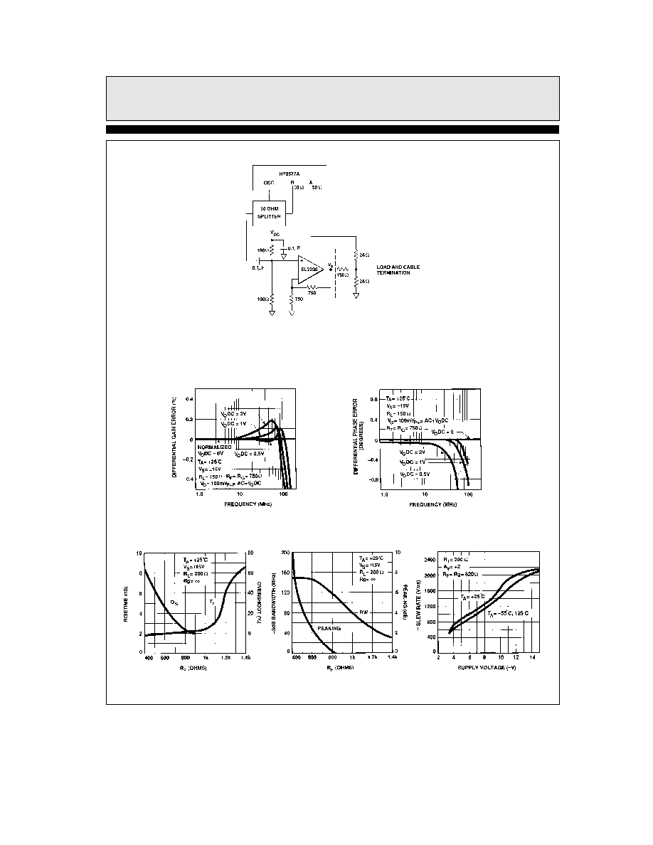
2030 ≠ 5
Figure 1 NTSC Video Differential Gain and Phase Test Set-Up
vs Load Resistance Gain e a1
Differential Gain and Phase
vs Load Capacitance Gain e a1
Differential Gain and Phase
vs Supply Voltage Gain e a1
Differential Gain and Phase
vs Load Resistance Gain e a2
Differential Gain and Phase
vs Load Capacitance Gain e a2
Differential Gain and Phase
vs Supply Voltage Gain e a2
Differential Gain and Phase
2030 ≠ 6
4
EL2030C
120 MHz Current Feedback Amplifier
Typical Performance Curves
Contd
2030 ≠ 7
Figure 2 HDTV and Wideband Video Differential Gain and Phase Test Set-Up
DC Output Levels
vs Frequency for Various
Differential Gain Error
DC Output Levels
vs Frequency for Various
Differential Phase Error
for A
V
e
a
1
Risetime and Overshoot vs R
F
R
F
for A
V
e
a
1
Bandwidth and Peaking vs
g
Slew Rate vs Supply Voltage
2030 ≠ 8
5