 | –≠–ª–µ–∫—Ç—Ä–æ–Ω–Ω—ã–π –∫–æ–º–ø–æ–Ω–µ–Ω—Ç: EL2045CS | –°–∫–∞—á–∞—Ç—å:  PDF PDF  ZIP ZIP |
EL2045C
December
1995
Rev
C
EL2045C
Low-Power 100 MHz Gain-of-2 Stable Operational Amplifier
Note All information contained in this data sheet has been carefully checked and is believed to be accurate as of the date of publication however this data sheet cannot be a ``controlled document'' Current revisions if any to these
specifications are maintained at the factory and are available upon your request We recommend checking the revision level before finalization of your design documentation
1992 Elantec Inc
Features
100 MHz gain-bandwidth
product
Gain-of-2 stable
Low supply current
e
5 2 mA at V
S
e
g
15V
Wide supply range
e
g
2V to
g
18V dual-supply
e
2 5V to 36V single-supply
High slew rate
e
275 V
ms
Fast settling
e
80 ns to 0 1% for
a 10V step
Low differential gain
e
0 02% at
A
V
e a
2 R
L
e
150
X
Low differential phase
e
0 07 at
A
V
e a
2 R
L
e
150
X
Stable with unlimited capacitive
load
Wide output voltage swing
e
g
13 6V with V
S
e
g
15V
R
L
e
1000
X
e
3 8V 0 3V with V
S
e a
5V
R
L
e
500
X
Applications
Video amplifier
Single-supply amplifier
Active filters integrators
High-speed sample-and-hold
High-speed signal processing
ADC DAC buffer
Pulse RF amplifier
Pin diode receiver
Log amplifier
Photo multiplier amplifier
Difference amplifier
Ordering Information
Part No
Temp Range
Package
Outline
EL2045CN
0 C to
a
75 C
8-Pin P-DIP
MDP0031
EL2045CS
0 C to
a
75 C
8-Lead SO
MDP0027
General Description
The EL2045C is a high speed low power low cost monolithic
operational amplifier built on Elantec's proprietary comple-
mentary bipolar process The EL2045C is gain-of-2 stable and
features a 275 V
ms slew rate and 100 MHz gain-bandwidth
product while requiring only 5 2 mA of supply current
The power supply operating range of the EL2045C is from
g
18V down to as little as
g
2V For single-supply operation
the EL2045C operates from 36V down to as little as 2 5V The
excellent power supply operating range of the EL2045C makes
it an obvious choice for applications on a single
a
5V or
a
3V
supply
The EL2045C also features an extremely wide output voltage
swing of
g
13 6V with V
S
e
g
15V and R
L
e
1000
X At
g
5V
output voltage swing is a wide
g
3 8V with R
L
e
500
X and
g
3 2V with R
L
e
150
X Furthermore for single-supply opera-
tion at
a
5V output voltage swing is an excellent 0 3V to 3 8V
with R
L
e
500
X
At a gain of
a
2 the EL2045C has a
b
3 dB bandwidth of
100 MHz with a phase margin of 50
It can drive unlimited
load capacitance and because of its conventional voltage-feed-
back topology the EL2045C allows the use of reactive or non-
linear elements in its feedback network This versatility com-
bined with low cost and 75 mA of output-current drive makes
the EL2045C an ideal choice for price-sensitive applications re-
quiring low power and high speed
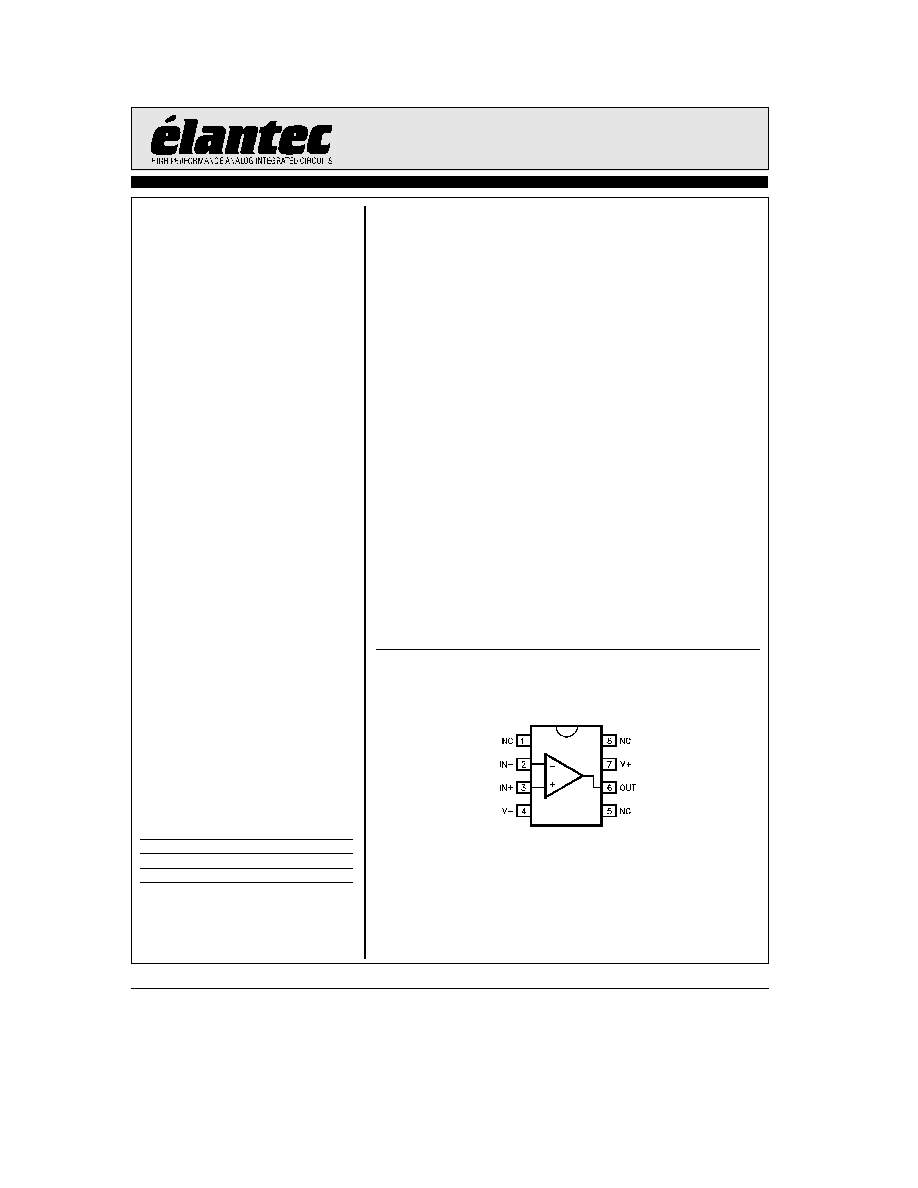
Connection Diagram
DIP and SO Package
2045 ≠ 1
EL2045C
Low-Power 100 MHz Gain-of-2 Stable Operational Amplifier
Absolute Maximum Ratings
(T
A
e
25 C)
Supply Voltage (V
S
)
g
18V or 36V
Peak Output Current (I
OP
)
Short-Circuit Protected
Output Short-Circuit Duration
Infinite
(Note 1)
Input Voltage (V
IN)
g
V
S
Differential Input Voltage (dV
IN
)
g
10V
Power Dissipation (P
D
)
See Curves
Operating Temperature
Range (T
A
)
0 C to
a
75 C
Operating Junction
Temperature (T
J
)
150 C
Storage Temperature (T
ST
)
b
65 C to
a
150 C
Important Note
All parameters having Min Max specifications are guaranteed The Test Level column indicates the specific device testing actually
performed during production and Quality inspection Elantec performs most electrical tests using modern high-speed automatic test
equipment specifically the LTX77 Series system Unless otherwise noted all tests are pulsed tests therefore T
J
e
T
C
e
T
A
Test Level
Test Procedure
I
100% production tested and QA sample tested per QA test plan QCX0002
II
100% production tested at T
A
e
25 C and QA sample tested at T
A
e
25 C
T
MAX
and T
MIN
per QA test plan QCX0002
III
QA sample tested per QA test plan QCX0002
IV
Parameter is guaranteed (but not tested) by Design and Characterization Data
V
Parameter is typical value at T
A
e
25 C for information purposes only
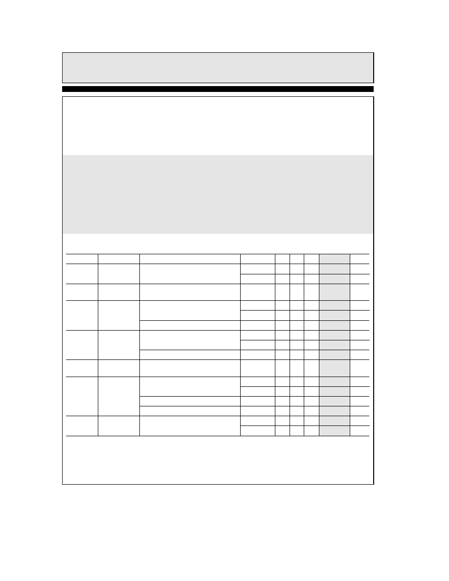
DC Electrical Characteristics
V
S
e
g
15V R
L
e
1000
X unless otherwise specified
Parameter
Description
Condition
Temp
Min Typ Max Test Level Units
V
OS
Input Offset
V
S
e
g
15V
25 C
0 5
7 0
I
mV
Voltage
T
MIN
T
MAX
9 0
III
mV
TCV
OS
Average Offset
(Note 2)
All
10 0
V
mV C
Voltage Drift
I
B
Input Bias
V
S
e
g
15V
25 C
2 8
8 2
I
mA
Current
T
MIN
T
MAX
9 2
III
mA
V
S
e
g
5V
25 C
2 8
V
mA
I
OS
Input Offset
V
S
e
g
15V
25 C
50
300
I
nA
Current
T
MIN
T
MAX
400
III
nA
V
S
e
g
5V
25 C
50
V
nA
TCI
OS
Average Offset
(Note 2)
All
0 3
V
nA C
Current Drift
A
VOL
Open-Loop Gain V
S
e
g
15V V
OUT
e
g
10V R
L
e
1000
X
25 C
1500 3000
I
V V
T
MIN
T
MAX
1500
III
V V
V
S
e
g
5V V
OUT
e
g
2 5V R
L
e
500
X
25 C
2500
V
V V
V
S
e
g
5V V
OUT
e
g
2 5V R
L
e
150
X
25 C
1750
V
V V
PSRR
Power Supply
V
S
e
g
5V to
g
15V
25 C
65
85
I
dB
Rejection Ratio
T
MIN
T
MAX
60
III
dB
2
TD
is
35in
EL2045C
Low-Power 100 MHz Gain-of-2 Stable Operational Amplifier
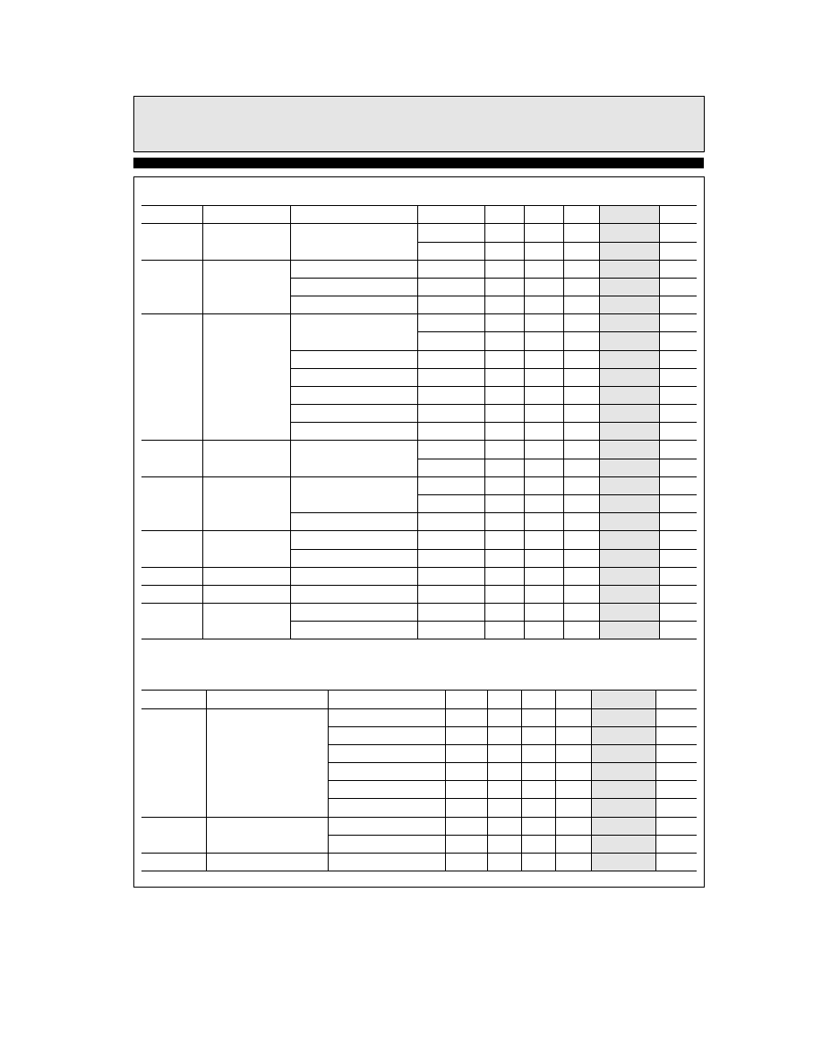
DC Electrical Characteristics
V
S
e
g
15V R
L
e
1000
X unless otherwise specified
Contd
Parameter
Description
Condition
Temp
Min
Typ
Max
Test Level
Units
CMRR
Common-Mode
V
CM
e
g
12V V
OUT
e
0V
25 C
70
95
I
dB
Rejection Ratio
T
MIN
T
MAX
70
III
dB
CMIR
Common-Mode
V
S
e
g
15V
25 C
g
14 0
V
V
Input Range
V
S
e
g
5V
25 C
g
4 2
V
V
V
S
e a
5V
25 C
4 2 0 1
V
V
V
OUT
Output Voltage
V
S
e
g
15V R
L
e
1000
X
25 C
g
13 4
g
13 6
I
V
Swing
T
MIN
T
MAX
g
13 1
III
V
V
S
e
g
15V R
L
e
500
X
25 C
g
12 0
g
13 4
I
V
V
S
e
g
5V R
L
e
500
X
25 C
g
3 4
g
3 8
IV
V
V
S
e
g
5V R
L
e
150
X
25 C
g
3 2
V
V
V
S
e a
5V R
L
e
500
X
25 C
3 6 0 4
3 8 0 3
I
V
T
MIN
T
MAX
3 5 0 5
III
V
I
SC
Output Short
25 C
40
75
I
mA
Circuit Current
T
MIN
T
MAX
35
III
mA
I
S
Supply Current
V
S
e
g
15V No Load
25 C
5 2
7
I
mA
T
MIN
T
MAX
7 6
III
mA
V
S
e
g
5V No Load
25 C
5 0
V
mA
R
IN
Input Resistance
Differential
25 C
150
V
k
X
Common-Mode
25 C
15
V
M
X
C
IN
Input Capacitance
A
V
e a
2
10 MHz
25 C
1 0
V
pF
R
OUT
Output Resistance
A
V
e a
2
25 C
50
V
m
X
PSOR
Power-Supply
Dual-Supply
25 C
g
2 0
g
18 0
V
V
Operating Range
Single-Supply
25 C
2 5
36 0
V
V
Closed-Loop AC Electrical Characteristics
V
S
e
g
15V A
V
e a
2 R
f
e
R
g
e
1 k
X C
f
e
3 pF R
L
e
1000
X unless otherwise specified
Parameter
Description
Condition
Temp
Min
Typ
Max
Test Level
Units
BW
b
3 dB Bandwidth
V
S
e
g
15V A
V
e a
2
25 C
100
V
MHz
(V
OUT
e
0 4 V
PP
)
V
S
e
g
15V A
V
e b
1
25 C
75
V
MHz
V
S
e
g
15V A
V
e a
5
25 C
20
V
MHz
V
S
e
g
15V A
V
e a
10
25 C
10
V
MHz
V
S
e
g
15V A
V
e a
20
25 C
5
V
MHz
V
S
e
g
5V A
V
e a
2
25 C
75
V
MHz
GBWP
Gain-Bandwidth Product
V
S
e
g
15V
25 C
100
V
MHz
V
S
e
g
5V
25 C
75
V
MHz
PM
Phase Margin
R
L
e
1 k
X C
L
e
10 pF
25 C
50
V
3
TD
is
45in
TD
is
19in

EL2045C
Low-Power 100 MHz Gain-of-2 Stable Operational Amplifier
Closed-Loop AC Electrical Characteristics
V
S
e
g
15V A
V
e a
2 R
f
e
R
g
e
1 k
X C
f
e
3 pF R
L
e
1000
X unless otherwise specified
Contd
Parameter
Description
Condition
Temp
Min
Typ
Max
Test Level
Units
SR
Slew Rate (Note 3)
V
S
e
g
15V R
L
e
1000
X
25 C
200
275
I
V
ms
V
S
e
g
5V R
L
e
500
X
25 C
200
V
V
ms
FPBW
Full-Power Bandwidth
V
S
e
g
15V
25 C
3 2
4 4
I
MHz
(Note 4)
V
S
e
g
5V
25 C
12 7
V
MHz
t
r
t
f
Rise Time Fall Time
0 1V Output Step
25 C
3 0
V
ns
OS
Overshoot
0 1V Output Step
25 C
20
V
%
t
PD
Propagation Delay
25 C
2 5
V
ns
t
s
Settling to
a
0 1%
V
S
e
g
15V 10V Step
25 C
80
V
ns
(A
V
e a
2)
V
S
e
g
5V 5V Step
25 C
60
V
ns
dG
Differential Gain (Note 5)
NTSC PAL
25 C
0 02
V
%
dP
Differential Phase (Note 5)
NTSC PAL
25 C
0 07
V
eN
Input Noise Voltage
10 kHz
25 C
15 0
V
nV
0
Hz
iN
Input Noise Current
10 kHz
25 C
1 50
V
pA
0
Hz
CI STAB
Load Capacitance Stability
A
V
e a
2
25 C
Infinite
V
pF
Note 1 A heat-sink is required to keep junction temperature below absolute maximum when an output is shorted
Note 2 Measured from T
MIN
to T
MAX
Note 3 Slew rate is measured on rising edge
Note 4 For V
S
e
g
15V V
OUT
e
20 V
PP
For V
S
e
g
5V V
OUT
e
5 V
PP
Full-power bandwidth is based on slew rate
measurement using FPBW
e
SR (2
q
Vpeak)
Note 5 Video Performance measured at V
S
e
g
15V A
V
e
a
2 with 2 times normal video level across R
L
e
150
X This
corresponds to standard video levels across a back-terminated 75
X load For other values of R
L
see curves
EL2045C Test Circuit
2045 ≠ 2
4
TD
is
28in

EL2045C
Low-Power 100 MHz Gain-of-2 Stable Operational Amplifier
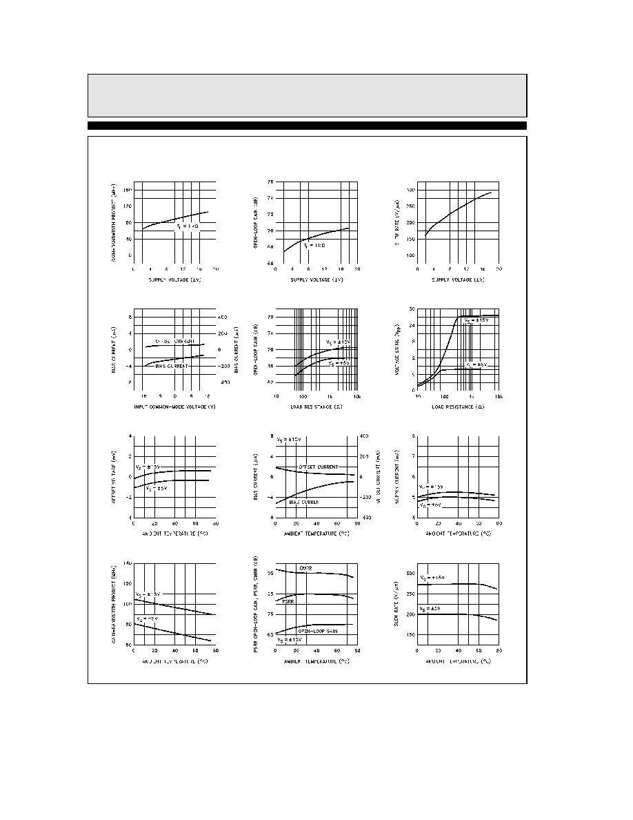
Typical Performance Curves
(T
A
e
25 C R
f
e
1 k
X C
f
e
3 pF R
L
e
1000
X A
V
e a
2 unless otherwise specified)
Frequency Response
Non-Inverting
Inverting Frequency Response
Various Load Resistances
Frequency Response for
Phase vs Frequency
Open-Loop Gain and
vs Frequency
Output Voltage Swing
Equivalent Input Noise
Output Resistance vs Frequency
CMRR PSRR and Closed-Loop
Distortion vs Frequency
2nd and 3rd Harmonic
Output Voltage Change
Settling Time vs
Supply Voltage
Supply Current vs
vs Supply Voltage
Common-Mode Input Range
vs Supply Voltage
Output Voltage Range
2045 ≠ 3
5
EL2045C
Low-Power 100 MHz Gain-of-2 Stable Operational Amplifier
Typical Performance Curves
(T
A
e
25 C R
f
e
1 k
X C
f
e
3 pF R
L
e
1000
X A
V
e a
2 unless otherwise specified)
Contd
vs Supply Voltage
Gain-Bandwidth Product
vs Supply Voltage
Open-Loop Gain
Supply Voltage
Slew-Rate vs
vs Input Common-Mode Voltage
Bias and Offset Current
vs Load Resistance
Open-Loop Gain
vs Load Resistance
Voltage Swing
vs Temperature
Offset Voltage
Current vs Temperature
Bias and Offset
vs Temperature
Supply Current
vs Temperature
Gain-Bandwidth Product
and CMRR vs Temperature
Open-Loop Gain PSRR
Temperature
Slew Rate vs
2045 ≠ 4
6

EL2045C
Low-Power 100 MHz Gain-of-2 Stable Operational Amplifier
Typical Performance Curves
(T
A
e
25 C R
f
e
1 k
X C
f
e
3 pF R
L
e
1000
X A
V
e a
2 unless otherwise specified)
Contd
Short-Circuit Current
vs Temperature
Gain-Bandwidth Product
vs Load Capacitance
Overshoot vs
Load Capacitance
2045 ≠ 5
Small-Signal
Step Response
2045 ≠ 6
Large-Signal
Step Response
2045 ≠ 7
Offset at 3 58 MHz
Phase vs DC Input
Differential Gain and
Offset at 4 43 MHz
Phase vs DC Input
Differential Gain and
150X Loads at 3 58 MHz
Phase vs Number of
Differential Gain and
150X Loads at 4 43 MHz
Phase vs Number of
Differential Gain and
vs Ambient Temperature
Maximum Power Dissipation
8-Pin Plastic DIP
vs Ambient Temperature
Maximum Power Dissipation
8-Lead SO
2045 ≠ 8
7
EL2045C
Low-Power 100 MHz Gain-of-2 Stable Operational Amplifier
Simplified Schematic
2045 ≠ 9
8
EL2045C
Low-Power 100 MHz Gain-of-2 Stable Operational Amplifier
Burn-In Circuit
2045 ≠ 10
All Packages Use the Same Schematic
Applications Information
Product Description
The EL2045C is a low-power wideband gain-of-2
stable monolithic operational amplifier built on
Elantec's proprietary high-speed complementary
bipolar process The EL2045C uses a classical
voltage-feedback topology which allows it to be
used in a variety of applications where current-
feedback amplifiers are not appropriate because
of restrictions placed upon the feedback element
used with the amplifier The conventional topolo-
gy of the EL2045C allows for example a capaci-
tor to be placed in the feedback path making it
an excellent choice for applications such as active
filters sample-and-holds or integrators Similar-
ly because of the ability to use diodes in the feed-
back network the EL2045C is an excellent choice
for applications such as fast log amplifiers
Single-Supply Operation
The EL2045C has been designed to have a wide
input and output voltage range This design also
makes the EL2045C an excellent choice for sin-
gle-supply operation Using a single positive sup-
ply
the lower input voltage range is within
100 mV of ground (R
L
e
500
X) and the lower
output voltage range is within 300 mV of ground
Upper input voltage range reaches 4 2V and out-
put voltage range reaches 3 8V with a 5V supply
and R
L
e
500
X This results in a 3 5V output
swing on a single 5V supply This wide output
voltage range also allows single-supply operation
with a supply voltage as high as 36V or as low as
2 5V On a single 2 5V supply the EL2045C still
has 1V of output swing
Gain-Bandwidth Product and the
b
3 dB
Bandwidth
The EL2045C has a gain-bandwidth product of
100 MHz while using only 5 2 mA of supply cur-
rent For gains greater than 4 its closed-loop
b
3 dB bandwidth is approximately equal to the
gain-bandwidth product divided by the noise
gain of the circuit For gains less than 4 higher-
order poles in the amplifier's transfer function
contribute to even higher closed loop band-
widths For example the EL2045C has a
b
3 dB
bandwidth of 100 MHz at a gain of
a
2 dropping
to 20 MHz at a gain of
a
5 It is important to
note that the EL2045C has been designed so that
this ``extra'' bandwidth in low-gain applications
does not come at the expense of stability As seen
in the typical performance curves the EL2045C
in a gain of
a
2 only exhibits 1 0 dB of peaking
with a 1000
X load
Video Performance
An industry-standard method of measuring the
video distortion of a component such as the
EL2045C is to measure the amount of differential
gain (dG) and differential phase (dP) that it in-
troduces
To
make
these
measurements
a
0 286 V
PP
(40 IRE) signal is applied to the device
with 0V DC offset (0 IRE) at either 3 58 MHz for
NTSC or 4 43 MHz for PAL A second measure-
ment is then made at 0 714V DC offset (100
IRE)
Differential gain is a measure of the
change in amplitude of the sine wave and is mea-
sured in percent Differential phase is a measure
of the change in phase and is measured in de-
grees
For signal transmission and distribution a back-
terminated cable (75
X in series at the drive end
and 75
X to ground at the receiving end) is pre-
ferred since the impedance match at both ends
will absorb any reflections However when dou-
ble termination is used the received signal is
halved therefore a gain of 2 configuration is typi-
cally used to compensate for the attenuation
The EL2045C has been designed as an economi-
cal solution for applications requiring low video
distortion It has been thoroughly characterized
9

EL2045C
Low-Power 100 MHz Gain-of-2 Stable Operational Amplifier
Applications Information
Contd
for video performance in the topology described
above and the results have been included as typi-
cal dG and dP specifications and as typical per-
formance curves In a gain of
a
2 driving 150
X
with standard video test levels at the input the
EL2045C exhibits dG and dP of only 0 02% and
0 07 at NTSC and PAL Because dG and dP can
vary with different DC offsets the video per-
formance of the EL2045C has been characterized
over the entire DC offset range from
b
0 714V to
a
0 714V
For more information
refer to the
curves of dG and dP vs DC Input Offset
The output drive capability of the EL2045C al-
lows it to drive up to 2 back-terminated loads
with good video performance For more demand-
ing applications such as greater output drive or
better video distortion a number of alternatives
such as the EL2120 EL400 or EL2074 should be
considered
Output Drive Capability
The EL2045C has been designed to drive low im-
pedance loads It can easily drive 6 V
PP
into a
150
X load This high output drive capability
makes the EL2045C an ideal choice for RF IF
and video applications Furthermore the current
drive of the EL2045C remains a minimum of
35 mA at low temperatures The EL2045C is cur-
rent-limited at the output allowing it to with-
stand shorts to ground However power dissipa-
tion with the output shorted can be in excess of
the power-dissipation capabilities of the package
Capacitive Loads
For ease of use the EL2045C has been designed
to drive any capacitive load
However
the
EL2045C remains stable by automatically reduc-
ing its gain-bandwidth product as capacitive load
increases Therefore for maximum bandwidth
capacitive loads should be reduced as much as
possible or isolated via a series output resistor
(Rs) Similarly coax lines can be driven but best
AC performance is obtained when they are termi-
nated with their characteristic impedance so that
the capacitance of the coaxial cable will not add
to the capacitive load seen by the amplifier Al-
though stable with all capacitive loads
some
peaking still occurs as load capacitance increases
A series resistor at the output of the EL2045C
can be used to reduce this peaking and further
improve stability
Printed-Circuit Layout
The EL2045C is well behaved and easy to apply
in most applications However a few simple tech-
niques will help assure rapid high quality results
As with any high-frequency device good PCB
layout is necessary for optimum performance
Ground-plane construction is highly recommend-
ed as is good power supply bypassing A 0 1
mF
ceramic capacitor is recommended for bypassing
both supplies Lead lengths should be as short as
possible and bypass capacitors should be as close
to the device pins as possible For good AC per-
formance parasitic capacitances should be kept
to a minimum at both inputs and at the output
Resistor values should be kept under 5 k
X be-
cause of the RC time constants associated with
the parasitic capacitance Metal-film and carbon
resistors are both acceptable use of wire-wound
resistors is not recommended because of their
parasitic inductance Similarly capacitors should
be low-inductance for best performance
The EL2045C Macromodel
This macromodel has been developed to assist
the user in simulating the EL2045C with sur-
rounding circuitry It has been developed for the
PSPICE simulator (copywritten by the Microsim
Corporation) and may need to be rearranged for
other simulators It approximates DC AC and
transient response for resistive loads but does
not accurately model capacitive loading
This
model is slightly more complicated than the
models used for low-frequency op-amps but it is
much more accurate for AC analysis
The model does not simulate these characteristics
accurately
noise
non-linearities
settling-time
temperature effects
CMRR
manufacturing variations
PSRR
10

EL2045C
Low-Power 100 MHz Gain-of-2 Stable Operational Amplifier
EL2045C Macromodel
Contd
Connections
a
input
Models
l
b
input
model qn npn(is
e
800E
b
18 bf
e
200 tf
e
0 2nS)
l
l
a
Vsupply
model qpa pnp(is
e
864E
b
18 bf
e
100 tf
e
0 2nS)
l
l
l
b
Vsupply
model qp pnp(is
e
800E
b
18 bf
e
125 tf
e
0 2nS)
l
l
l
l
output
ends
l
l
l
l
l
subckt M2045
3
2
7
4
6
Input stage
ie 7 37 0 9mA
r6 36 37 400
r7 38 37 400
rc1 4 30 850
rc2 4 39 850
q1 30 3 36 qp
q2 39 2 38 qpa
ediff 33 0 39 30 1 0
rdiff 33 0 1Meg
Compensation Section
ga 0 34 33 0 1m
rh 34 0 2Meg
ch 34 0 1 5pF
rc 34 40 1K
cc 40 0 1pF
Poles
ep 41 0 40 0 1
rpa 41 42 200
cpa 42 0 2pF
rpb 42 43 200
cpb 43 0 2pF
Output Stage
ios1 7 50 1 0mA
ios2 51 4 1 0mA
q3 4 43 50 qp
q4 7 43 51 qn
q5 7 50 52 qn
q6 4 51 53 qp
ros1 52 6 25
ros2 6 53 25
Power Supply Current
ips 7 4 2 7mA
11
TAB
WIDE
TD
is
07in
TD
is
07in
EL2045C
December
1995
Rev
C
EL2045C
Low-Power 100 MHz Gain-of-2 Stable Operational Amplifier
EL2045C Macromodel
Contd
2045 ≠ 11
EL2045C Model
General Disclaimer
Specifications contained in this data sheet are in effect as of the publication date shown Elantec Inc reserves the right to make changes
in the circuitry or specifications contained herein at any time without notice Elantec Inc assumes no responsibility for the use of any
circuits described herein and makes no representations that they are free from patent infringement
Elantec Inc
1996 Tarob Court
Milpitas CA 95035
Telephone (408) 945-1323
(800) 333-6314
Fax (408) 945-9305
European Office 44-71-482-4596
WARNING
Life Support Policy
Elantec Inc products are not authorized for and should not be
used within Life Support Systems without the specific written
consent of Elantec Inc Life Support systems are equipment in-
tended to support or sustain life and whose failure to perform
when properly used in accordance with instructions provided can
be reasonably expected to result in significant personal injury or
death Users contemplating application of Elantec Inc products
in Life Support Systems are requested to contact Elantec Inc
factory headquarters to establish suitable terms
conditions for
these applications Elantec Inc 's warranty is limited to replace-
ment of defective components and does not cover injury to per-
sons or property or other consequential damages
Printed in U S A
12