
EL2071CEL2171C
December
1995
Rev
E
EL2071C EL2171C
150 MHz Current Feedback Amplifier
Note All information contained in this data sheet has been carefully checked and is believed to be accurate as of the date of publication however this data sheet cannot be a ``controlled document'' Current revisions if any to these
specifications are maintained at the factory and are available upon your request We recommend checking the revision level before finalization of your design documentation
1991 Elantec Inc
Features
150 MHz
b
3 dB bandwidth
A
V
e
20
10 ns settling to 0 1%
V
S
e
g
5V
15 mA
2 5 ns rise fall times (2V step)
Overload short-circuit protected
g
7 to
g
50 closed-loop gain
range
Low cost
EL2171 is direct replacement for
CLC401
Disable capability on EL2071
Applications
Line drivers
DC-coupled log amplifiers
High-speed modems radios
High-speed A D conversion
D A I-V conversion
Photodiode CCD preamps
IF processors
High-speed communications
Analog multiplexing
(using disable
EL2071)
Power down mode
(using disable
EL2071)
Ordering Information
Part No
Temp Range
Package
Outline
EL2171CN
b
40 C to
a
85 C 8-Pin P-DIP MDP0031
EL2171CS
b
40 C to
a
85 C 8-Lead SO
MDP0027
EL2071CN
b
40 C to
a
85 C 8-Pin P-DIP MDP0031
EL2071CS
b
40 C to
a
85 C 8-Lead SO
MDP0027
General Description
The EL2071 and EL2171 are wide bandwidth fast settling
monolithic amplifiers built using an advanced complementary
bipolar process The EL2071 has a disable enable feature which
allows power down and analog multiplexing These amplifiers
use current-mode feedback to achieve more bandwidth at a giv-
en gain than conventional operational amplifiers Designed for
closed-loop gains of
g
7 to
g
50 the EL2071 and EL2171 have a
150 MHz
b
3 dB bandwidth (A
V
e
a
20) and 2 5 ns rise fall
time while consuming only 15 mA of supply current The
EL2071 consumes only 1 5 mA when disabled
The wide 150 MHz bandwidth and extremely linear phase
(0 2 dB deviation from linear at 50 MHz) allow superior signal
fidelity These features make the EL2071 and EL2171 especially
suited for many digital communication system applications
The EL2071's and EL2171's settling to 0 1% in 10 ns and ability
to drive capacitive loads make them ideal in flash A D applica-
tions D A systems can also benefit from the EL2071 and
EL2171 especially if linearity and drive levels are important
Elantec products and facilities comply with MIL-I-45208A and
other applicable quality specifications
For information on
Elantec's processing see Elantec document QRA-1 Elantec's
Processing Monolithic Integrated Circuits
Connection Diagrams
EL2171
DIP and SO Package
2071 � 1
Top View
EL2071
DIP and SO Package
2071 � 2
Top View
Manufactured under U S Patent No 4 893 091
EL2071C EL2171C
150 MHz Current Feedback Amplifier
Absolute Maximum Ratings
(T
A
e
25 C)
Supply Voltage (V
S
)
g
7V
Output Current
Output is short-circuit protect-
ed to ground however maxi-
mum reliability is obtained if
I
OUT
does not exceed 70 mA
Common Mode Input Voltage
g
V
S
Differential Input Voltage
5V
Power Dissipation
See Curves
Operating Temperature
b
40 C to
a
85 C
Operating Junction Temperature
Ceramic Packages
175 C
Plastic Packages
150 C
Storage Temperature
b
60 C to
a
150 C
Important Note
All parameters having Min Max specifications are guaranteed The Test Level column indicates the specific device testing actually
performed during production and Quality inspection Elantec performs most electrical tests using modern high-speed automatic test
equipment specifically the LTX77 Series system Unless otherwise noted all tests are pulsed tests therefore T
J
e
T
C
e
T
A
Test Level
Test Procedure
I
100% production tested and QA sample tested per QA test plan QCX0002
II
100% production tested at T
A
e
25 C and QA sample tested at T
A
e
25 C
T
MAX
and T
MIN
per QA test plan QCX0002
III
QA sample tested per QA test plan QCX0002
IV
Parameter is guaranteed (but not tested) by Design and Characterization Data
V
Parameter is typical value at T
A
e
25 C for information purposes only
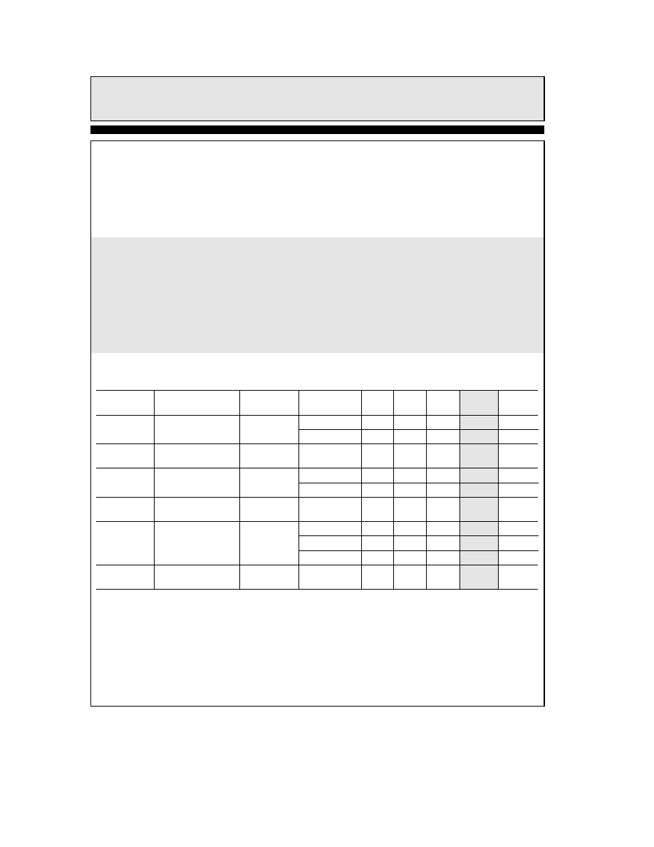
Open Loop DC Electrical Characteristics
V
S
e
g
5V R
L
e
100
X unless otherwise specified
Parameter
Description
Test
Temp
Min
Typ
Max
Test
Units
Conditions
Level
V
OS
Input Offset Voltage
25 C
3
6
I
mV
T
MIN
T
MAX
10
III
mV
TC V
OS
Average Offset
(Note 1)
All
20
50
IV
mV C
Voltage Drift
a
I
IN
a
Input Current
25 C T
MAX
10
20
II
mA
T
MIN
36
III
mA
TC (
a
I
IN
)
Average
a
Input
(Note 1)
All
100
200
IV
nA C
Current Drift
b
I
IN
b
Input Current
25 C
10
30
I
mA
T
MIN
46
III
mA
T
MAX
40
III
mA
TC (
b
I
IN
)
Average
b
Input
(Note 1)
All
100
200
IV
nA C
Current Drift
2
TD
is
08in
TD
is
26in
EL2071C EL2171C
150 MHz Current Feedback Amplifier
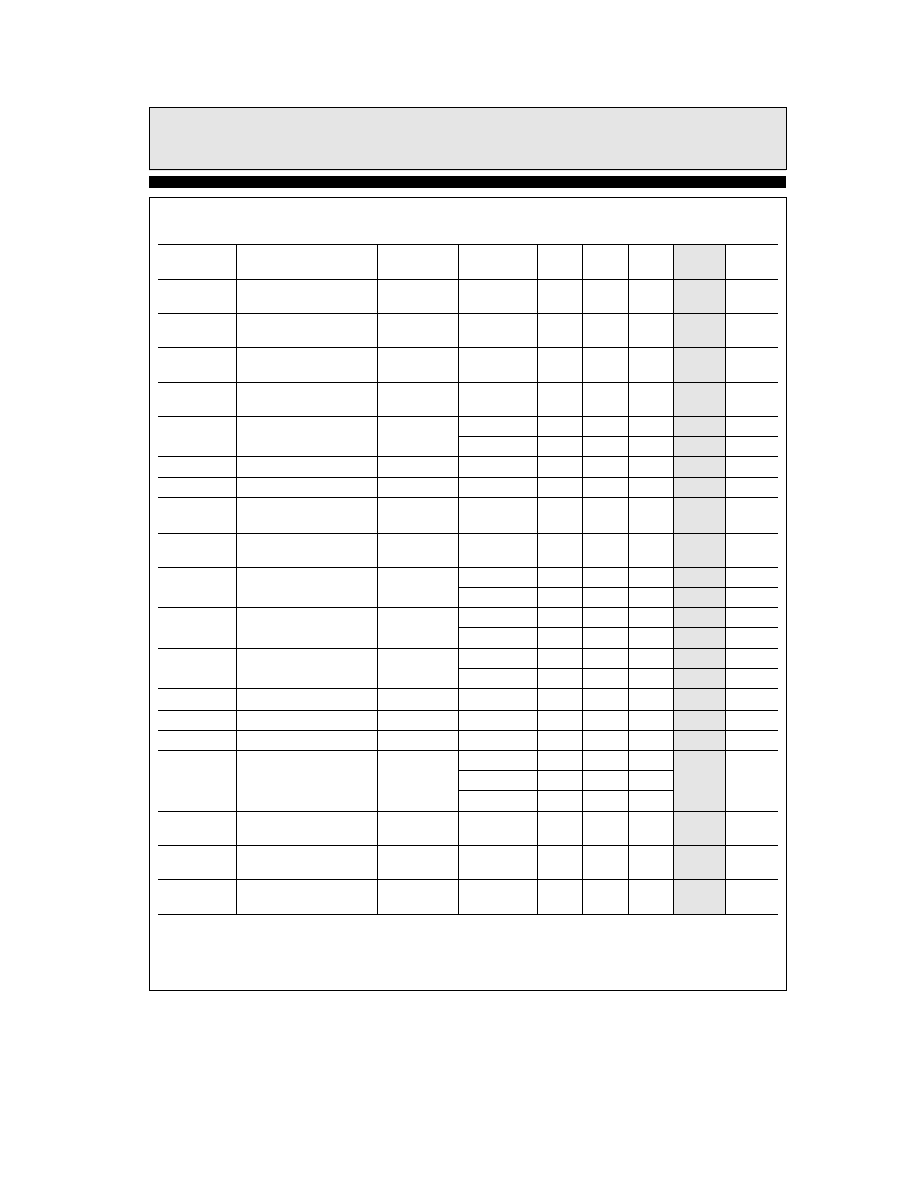
Open Loop DC Electrical Characteristics
V
S
e
g
5V R
L
e
100
X unless otherwise specified
Contd
Parameter
Description
Test
Temp
Min
Typ
Max
Test
Units
Conditions
Level
PSRR
Power Supply
(Note 2)
All
50
55
II
dB
Rejection Ratio
CMRR
Common-Mode
All
40
50
II
dB
Rejection Ratio
I
S
Supply Current
No Load
All
15
21
II
mA
Quiescent
I
SOFF
Supply Current
EL2071C
All
1 5
3 0
II
mA
Disabled
(Note 3)
a
R
IN
a
Input Resistance
25 C T
MAX
100
200
II
k
X
T
MIN
50
III
k
X
C
IN
Input Capacitance
All
0 5
2 5
IV
pF
R
OUT
Output Resistance (DC)
All
0 2
0 3
IV
X
R
OUTD
Output Resistance (DC)
EL2071C
All
100
200
IV
k
X
Disabled
C
OUTD
Output Capacitance (DC)
EL2071C
All
0 5
2 0
IV
pF
Disabled
CMIR
Common-Mode Input
(Note 4)
25 C T
MAX
g
2 5
g
2 8
IV
V
Range
T
MIN
g
2
IV
V
I
OUT
Output Current
25 C T
MAX
50
70
II
mA
T
MIN
35
III
mA
V
OUT
Output Voltage Swing
No Load
25 C T
MAX
3 2
3 5
II
V
T
MIN
3
II
V
V
OUTL
Output Voltage Swing
R
L
e
100
X
25 C
3 2
3 4
I
V
R
OL
Transimpedance
25 C
250
1000
I
V mA
I
LOGIC
Pin 8 Current
a
5V
EL2071C
All
500
750
II
mA
V
DIS
Minimum Pin 8
EL2071C
25 C
4 3
V to Disable
T
MIN
4 0
II
V
T
MAX
4 6
V
EN
Maximum Pin 8
EL2071C
All
0 7
II
V
V to Enable
I
DIS
Minimum Pin 8
EL2071C
All
750
II
mA
I to Disable
I
EN
Maximum Pin 8
EL2071C
All
35
II
mA
I to Enable
3
TD
is
62in

EL2071C EL2171C
150 MHz Current Feedback Amplifier
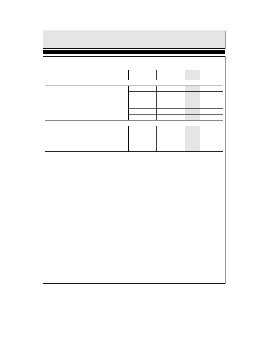
Closed Loop AC Electrical Characteristics
V
S
e
g
5V R
F
e
1 5 k
X A
V
e a
20 R
L
e
100
X unless otherwise specified
Parameter
Description
Test
Temp
Min
Typ
Max
Test
Units
Conditions
Level
FREQUENCY RESPONSE
SSBW
b
3 dB Bandwidth
25 C
100
150
V
MHz
(V
OUT
k
2 0 V
PP
)
T
MIN
100
V
MHZ
T
MAX
70
V
MHz
LSBW
b
3 dB Bandwidth
25 C T
MIN
65
100
IV
MHz
(V
OUT
k
5 0 V
PP
)
T
MAX
55
IV
MHz
GAIN FLATNESS
GFPL
Peaking
k
25 MHz
25 C
0 0
0 1
V
dB
V
OUT
k
2 0 V
PP
T
MIN
T
MAX
0 1
V
dB
GFPH
Peaking
l
25 MHz
25 C
0 0
0 2
V
dB
V
OUT
k
2 0 V
PP
T
MIN
T
MAX
0 2
V
dB
GFR
Rolloff
k
50 MHz
25 C
0 2
1 0
V
dB
V
OUT
k
2 0 V
PP
T
MIN
1 0
V
dB
T
MAX
1 3
V
dB
LPD
Linear Phase Deviation
k
50 MHz
25 C T
MIN
0 2
1 0
IV
V
OUT
k
2 0 V
PP
T
MAX
1 5
IV
TIME-DOMAIN RESPONSE
t
r1
t
f1
Rise Time Fall Time
2 0V Step
25 C T
MIN
2 5
3 5
IV
ns
T
MAX
5
IV
ns
t
r2
t
f2
Rise Time Fall Time
5 0V Step
25 C T
MIN
5
7
IV
ns
T
MAX
8
IV
ns
t
s
Settling Time to 0 1%
2 0V Step
All
10
15
IV
ns
OS
Overshoot
2 0V Step
All
0
10
IV
%
SR
Slew Rate
25 C T
MIN
800
1200
IV
V
ms
T
MAX
700
IV
V
ms
DISTORTION
HD2
2nd Harmonic
2 V
PP
25 C
b
45
b
35
V
dBc
Distortion
20 MHz
T
MIN
T
MAX
b
35
V
dBc
HD3
3rd Harmonic
2 V
PP
25 C
b
60
b
50
V
dBc
Distortion
20 MHz
T
MIN
b
50
V
dBc
T
MAX
b
45
V
dBc
4
TD
is
61in
EL2071C EL2171C
150 MHz Current Feedback Amplifier
Closed Loop AC Electrical Characteristics
V
S
e
g
5V R
F
e
1 5 k
X A
V
e a
20 R
L
e
100
X unless otherwise specified
Contd
Parameter
Description
Test
Temp
Min
Typ
Max
Test
Units
Conditions
Level
EQUIVALENT INPUT NOISE
NF
Noise Floor
l
100 kHz
25 C
b
158
b
155
IV
dBm (1 Hz)
T
MIN
b
155
IV
dBm (1 Hz)
T
MAX
b
154
IV
dBm (1 Hz)
INV
Integrated Noise
25 C
35
50
IV
mV
100 kHz to 200 MHz
T
MIN
50
IV
mV
T
MAX
55
IV
mV
DISABLE ENABLE PERFORMANCE
EL2071C
T
OFF
V
OUT
e
2 V
PP
20 MHz
Disable Time
All
70
200
IV
ns
to
l
40 dB
T
ON
Enable Time
All
40
100
IV
ns
ISO
Off Isolation
20 MHz
All
50
55
IV
dB
Note 1 Measured from T
MIN
to T
MAX
Note 2 PSRR is measured at V
S
e
g
4 5V and V
S
e
g
5 5V Both supplies are changed simultaneously
Note 3 Supply current when disabled is measured at the negative supply
Note 4 Common-Mode Input Range for Rated Performance
5
TD
is
26in