 | –≠–ª–µ–∫—Ç—Ä–æ–Ω–Ω—ã–π –∫–æ–º–ø–æ–Ω–µ–Ω—Ç: EL2074CS | –°–∫–∞—á–∞—Ç—å:  PDF PDF  ZIP ZIP |
Note: All information contained in this data sheet has been carefully checked and is believed to be accurate as of the date of publication; however, this data sheet cannot be a "controlled document". Current revisions, if any, to these
specifications are maintained at the factory and are available upon your request. We recommend checking the revision level before finalization of your design documentation.
© 2001 Elantec Semiconductor, Inc.
E
L
2
0
7
4
C
General Description
The EL2074C is a precision voltage-feedback amplifier featuring a
400MHz gain-bandwidth product, fast settling time, excellent differ-
ential gain and differential phase performance, and a minimum of
50mA output current drive over temperature.
The EL2074C is gain-of-2 stable with a -3dB bandwidth of 400MHz
at A
V
= +2. It has a very low 200µV of input offset voltage, only 2µA
of input bias current, and a fully symmetrical differential input. Like
all voltage-feedback operational amplifiers, the EL2074C allows the
use of reactive or non-linear components in the feedback loop. This
combination of speed and versatility makes the EL2074C the ideal
choice for all op-amp applications at a noise gain of 2 or greater
requiring high speed and precision, including active filters, integra-
tors, sample-and-holds, and log amps. The low distortion, high output
current, and fast settling makes the EL2074C an ideal amplifier for
signal-processing and digitizing systems.
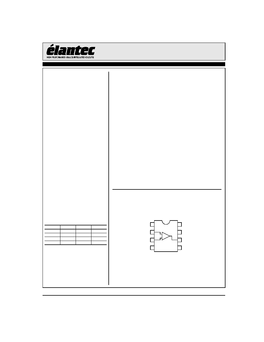
Connection Diagram
1
2
3
4
8
7
6
5
EL2074C
(8-Pin SO & 8-Pin PDIP)
NC
IN-
IN+
V-
NC
V+
OUT
NC
-
+
Features
∑ 400MHz gain-bandwidth product
∑ Gain-of-2 stable
∑ Ultra low video distortion =
0.01%/0.015∞ @NTSC/PAL
∑ Conventional voltage-feedback
topology
∑ Low offset voltage = 200µV
∑ Low bias current = 2µA
∑ Low offset current = 0.1µA
∑ Output current = 50mA over
temperature
∑ Fast settling = 13ns to 0.1%
∑ Low distortion = -55dB HD2,
------
-70dB HD3 @20MHz, 2V
PP
, A
V
=
+2
Applications
∑ High resolution video
∑ Active filters/integrators
∑ High-speed signal processing
∑ ADC/DAC buffers
∑ Pulse/RF amplifiers
∑ Pin diode receivers
∑ Log amplifiers
∑ Photo multiplier amplifiers
∑ High speed sample-and-holds
Ordering Information
Part No.
Package
Tape & Reel
Outline #
EL2074CN
8-Pin PDIP
-
MDP0031
EL2074CS
8-Pin SO
-
MDP0027
EL2074CS-T7
8-Pin SO
7"
MDP0027
EL2074CS-T13
8-Pin SO
13"
MDP0027
EL2074C
400MHz GBWP Gain-of-2 Stable Operational Amplifier
S
e
p
t
e
m
b
e
r
2
6
,
2
0
0
1

2
EL2074C
400MHz GBWP Gain-of-2 Stable Operational Amplifier
E
L
2
0
7
4
C
Absolute Maximum Ratings
(T
A
= 25∞C)
Supply Voltage (V
S
)
±7V
Output Current Output is short-circuit protected to ground, however,
maximum reliability is obtained if I
OUT
does not exceed 70mA.
Common-Mode Input
±V
S
Differential Input Voltage
5V
Thermal Resistance (PDIP)
JA
= 95∞C/W
Thermal Resistance (SO)
JA
= 175∞C/W
Operating Temperature
0∞C to +75∞C
Junction Temperature
175∞C
Storage Temperature
-60∞C to +150∞C
Note: See EL2071/EL2171 for Thermal Impedance curves
Important Note:
All parameters having Min/Max specifications are guaranteed. Typ values are for information purposes only. Unless otherwise noted, all tests are at the
specified temperature and are pulsed tests, therefore: T
J
= T
C
= T
A
.
Open Loop DC Electrical Characteristics
V
S
= ±5V, R
L
= 100
, unless otherwise specified.
Parameter
Description
Test Conditions
Temp
Min
Typ
Max
Unit
V
OS
Input Offset Voltage
V
CM
= 0V
25∞C
0.2
1.5
mV
T
MIN
, T
MAX
3
mV
TCV
OS
Average Offset
Voltage Drift
[1]
All
8
µV/∞C
I
B
Input Bias Current
V
CM
= 0V
All
2
6
µA
I
OS
Input Offset Current
V
CM
= 0V
25∞C
0.1
1
µA
T
MIN
, T
MAX
2
µA
PSRR
Power Supply Rejection Ratio
[2]
All
60
80
dB
CMRR
Common Mode Rejection Ratio
[3]
All
65
90
dB
I
S
Supply Current - Quiescent
No Load
25∞C
21
25
mA
T
MIN
, T
MAX
25
mA
R
IN
(diff)
R
IN
(Differential)
Open-Loop
25∞C
15
k
C
IN
(diff)
C
IN
(Differential)
Open-Loop
25∞C
1
pF
R
IN
(cm)
R
IN
(Common-Mode)
25∞C
1
M
C
IN
(cm)
C
IN
(Common-Mode)
25∞C
1
pF
R
OUT
Output Resistance
25∞C
20
m
CMIR
Common-Mode Input
Range
25∞C
±3
±3.5
V
T
MIN
, T
MAX
±2.5
V
I
OUT
Output Current
All
50
70
mA
V
OUT
Output Voltage Swing
No Load
All
±3.5
±4
V
V
OUT
100
Output Voltage Swing
100
All
±3
±3.6
V
V
OUT
50
Output Voltage Swing
50
All
±2.5
±3.4
V
A
VOL
100
Open-Loop Gain
100
25∞C
500
1000
V/V
T
MIN
, T
MAX
400
V/V
A
VOL
50
Open-Loop Gain
50
25∞C
400
800
V/V
T
MIN
, T
MAX
300
V/V
eN@ > 1MHz
Noise Voltage 1MHz to 100MHz
25∞C
2.3
nV/
Hz
iN@ > 100kHz
Noise Current 100kHz to 100MHz
25∞C
3.2
pA/
Hz
1. Measured from T
MIN
, T
MAX
2. ±V
CC
= ±4.5V to 5.5V
3. ±V
IN
= ±2.5V, V
OUT
= 0V

3
EL2074C
400MHz GBWP Gain-of-2 Stable Operational Amplifier
E
L
2
0
7
4
C
Closed Loop AC Electrical Characteristics
V
S
= ±5V, A
V
= +2, R
F
= R
G
= 250
, C
F
= 3pF, R
L
= 100
unless otherwise specified.
Parameter
Description
Test Conditions
Temp
Min
Typ
Max
Unit
SSBW
-3dB Bandwidth
A
V
= -1
25∞C
400
MHz
(V
OUT
= 0.4V
PP
)
A
V
= +2
25∞C
250
400
MHz
T
MIN
, T
MAX
250
MHz
A
V
= +5
25∞C
100
MHz
A
V
= +10
25∞C
40
MHz
GBWP
Gain-Bandwidth Product
A
V
= +10
25∞C
400
MHz
LSBWa
-3dB Bandwidth
V
OUT
= 2V
PP
[1]
All
43
63
MHz
LSBWb
-3dB Bandwidth
V
OUT
= 5V
PP
[1]
All
17
25
MHz
GFPL
Peaking (<50MHz)
V
OUT
= 0.4V
PP
25∞C
0
1
dB
T
MIN
, T
MAX
1
dB
GFPH
Peaking (>50MHz)
V
OUT
= 0.4V
PP
25∞C
0
2
dB
T
MIN
, T
MAX
2
dB
GFR
Rolloff (<100MHz)
V
OUT
= 0.4V
PP
25∞C
0.1
0.5
dB
T
MIN
, T
MAX
0.5
dB
LPD
Linear Phase Deviation (<100MHz)
V
OUT
= 0.4V
PP
All
1
1.8
∞
PM
Phase Margin
A
V
= +2
25∞C
50
∞
tr1, tf1
Rise Time, Fall Time
0.4V Step, A
V
= +2
25∞C
1.8
ns
tr2, tf2
Rise Time, Fall Time
5V Step, A
V
= +2
25∞C
8
ns
ts1
Settling to 0.1% (A
V
= -1)
2V Step
25∞C
13
ns
ts2
Settling to 0.01% (A
V
= -1)
2V Step
25∞C
25
ns
OS
Overshoot
2V Step
25∞C
5
%
SR
Slew Rate
2V Step
All
275
400
V/µs
Distortion
[2]
HD2a
2nd Harmonic Distortion
@ 10MHz, A
V
= +2
25∞C
-65
-55
dBc
HD2c
2nd Harmonic Distortion
@ 20MHz, A
V
= +2
25∞C
-55
-45
dBc
T
MIN
, T
MAX
-45
dBc
HD3a
3rd Harmonic Distortion
@ 10MHz, A
V
= +2
25∞C
-72
-60
dBc
HD3c
3rd Harmonic Distortion
@ 20MHz, A
V
= +2
25∞C
-70
-60
dBc
T
MIN
, T
MAX
-60
dBc
Video Performance
[3]
dG
Differential Gain
NTSC
25∞C
0.01
0.05
%
pp
dP
Differential Phase
NTSC
25∞C
0.015
0.05
∞
pp
dG
Differential Gain
30MHz
25∞C
0.1
%
pp
dP
Differential Phase
30MHz
25∞C
0.1
∞
pp
VBW
±0.1 dB Bandwidth Flatness
25∞C
25
50
MHz
1. Large-signal bandwidth calculated using LSBW = Slew Rate / 2
V
PEAK
2. All distortion measurements are made with V
OUT
= 2V
PP
, R
L
= 100
3. Video performance measured at A
V
= +2 with 2 times normal video level across R
L
= 100
. This corresponds to standard video levels across a back-
terminated 50
load, i.e., 0≠100 IRE, 40IREpp giving a 1V
PP
video signal across the 50
load. For other values of R
L
, see curves

4
EL2074C
400MHz GBWP Gain-of-2 Stable Operational Amplifier
E
L
2
0
7
4
C
Typical Performance Curves
Non-Inverting Frequency
Response
Inverting Frequency Response
Frequency Response for Various
R
L
s
Open Loop Gain and Phase
Output Voltage Swing vs
Frequency
Equivalent Input Noise
PSRR, CMRR, and Closed-Loop
R
O
vs Frequency
2nd and 3rd Harmonic
Distortion vs Frequency
2-Tone, 3rd Order
Intermodulation Intercept

5
EL2074C
400MHz GBWP Gain-of-2 Stable Operational Amplifier
E
L
2
0
7
4
C
Series Resistor and Resulting
Bandwidth vs Capacitive Load
Settling Time vs
Output Voltage Change
Settling Time vs
Closed-Loop Gain
Supply Current
vs Temperature
Bias and Offset Current vs
Input Common-Mode Voltage
Common-Mode Rejection Ratio vs
Input Common-Mode Voltage
Bias and Offset Current vs
Temperature
Offset Voltage vs Temperature
A
VOL
, PSRR, and CMRR vs
Temperature