 | –≠–ª–µ–∫—Ç—Ä–æ–Ω–Ω—ã–π –∫–æ–º–ø–æ–Ω–µ–Ω—Ç: EL2099CT | –°–∫–∞—á–∞—Ç—å:  PDF PDF  ZIP ZIP |

EL2099C
January
1996
Rev
D
EL2099C
Video Distribution Amplifier
Note All information contained in this data sheet has been carefully checked and is believed to be accurate as of the date of publication however this data sheet cannot be a ``controlled document'' Current revisions if any to these
specifications are maintained at the factory and are available upon your request We recommend checking the revision level before finalization of your design documentation
1992 Elantec Inc
Features
50 MHz
b
3 dB bandwidth
A
V
e a
2
Differential gain 0 03%
Differential phase 0 05
Output short circuit current
800 mA
Can drive six 75X double
terminated cables
g
11V
Slew rate
e
1000V
ms
Wide supply voltage range
g
5V to
g
15V
Applications
Video line driver
ATE pin driver
High speed data acquisition
Ordering Information
Part No
Temp Range
Pkg
Outline
EL2099CT 0 C to a75 C 5-Pin TO-220 MDP0028
General Description
The EL2099C is a high speed monolithic operational amplifier
featuring excellent video performance and high output current
capability Built using Elantec's Complementary Bipolar pro-
cess the EL2099C uses current mode feedback to achieve wide
bandwidth and is stable in unity gain configuration
Operation from power supplies ranging from
g
5V to
g
15V
makes the EL2099C extremely versatile
With supplies at
g
15V the EL2099C can deliver
g
11V into 25
X at slew rates of
1000V
ms At
g
5V supplies output voltage range is
g
3V into
25
X Its speed and output current capability make this device
ideal for video line driver and automatic test equipment appli-
cations
Differential Gain and Phase of the EL2099C are 0 03% and
0 05 respectively and
b
3 dB bandwidth is 50 MHz These fea-
tures make the EL2099C especially well suited for video distri-
bution applications
Elantec products and facilities comply with MIL-I-45208A and
other applicable quality specifications
For information on
Elantec's processing see Elantec document QRA-1 Elantec's
Processing Monolithic Integrated Circuits
Connection Diagram
5-Pin TO-220
2099 ≠ 1
Manufactured under U S Patent Nos 5 179 355 4 893 091 U K Patent No
2261786

EL2099C
Video Distribution Amplifier
Absolute Maximum Ratings
(T
A
e
25 C)
Voltage between V
S
a
and V
S
b
a
33V
Voltage at V
S
a
a
16 5V
Voltage at V
S
b
b
16 5V
Voltage between V
INa
and V
INb
g
6V
Current into V
INa
or V
INb
g
10 mA
Internal Power Dissipation
See Curves
Operating Ambient Temperature Range
0 C to
a
75 C
Operating Junction Temperature
150 C
Storage Temperature Range
b
65 C to
a
150 C
Important Note
All parameters having Min Max specifications are guaranteed The Test Level column indicates the specific device testing actually
performed during production and Quality inspection Elantec performs most electrical tests using modern high-speed automatic test
equipment specifically the LTX77 Series system Unless otherwise noted all tests are pulsed tests therefore T
J
e
T
C
e
T
A
Test Level
Test Procedure
I
100% production tested and QA sample tested per QA test plan QCX0002
II
100% production tested at T
A
e
25 C and QA sample tested at T
A
e
25 C
T
MAX
and T
MIN
per QA test plan QCX0002
III
QA sample tested per QA test plan QCX0002
IV
Parameter is guaranteed (but not tested) by Design and Characterization Data
V
Parameter is typical value at T
A
e
25 C for information purposes only
Open Loop DC Electrical Characteristics
V
S
e
g
15V R
L
e
25
X T
A
e
25 C unless otherwise specified
Parameter
Description
Temp
Min
Typ
Max
Test
Units
Level
V
OS
Input Offset Voltage
25 C
5
20
I
mV
T
MIN
T
MAX
25
IV
mV
TC V
OS
Average Offset Voltage Drift
Full
20
V
mV C
a
I
IN
a
Input Current
25 C
5
20
I
mA
T
MIN
T
MAX
30
IV
mA
b
I
IN
b
Input Current
25 C
8
35
I
mA
T
MIN
T
MAX
50
IV
mA
CMRR
Common Mode Rejection
25 C
50
60
I
dB
Ratio (Note 1)
PSRR
Power Supply Rejection
25 C
60
70
I
dB
Ratio (Note 2)
R
OL
Transimpedance
25 C
85
140
I
k
X
a
R
IN
a
Input Resistance
25 C
700
1000
I
k
X
(Note 3)
T
MIN
T
MAX
600
IV
k
X
a
C
IN
a
Input Capacitance
25 C
3
V
pF
CMIR
Common Mode Input Range
25 C
g
12 5
V
V
2
TD
is
32in

EL2099C
Video Distribution Amplifier
Open Loop DC Electrical Characteristics
Contd
V
S
e
g
15V R
L
e
25
X T
A
e
25 C unless otherwise specified
Parameter
Description
Temp
Min
Typ
Max
Test
Units
Level
V
O
Output Voltage Swing
25 C
g
9
g
11
I
V
V
S
e
g
15V
Output Voltage Swing
25 C
g
2 4
g
3 0
I
V
V
S
e
g
5V
I
OUT
Output Current
25 C
360
440
I
mA
I
SC
Output Short-Circuit
25 C
600
800
I
mA
Current
T
MIN
T
MAX
800
V
mA
I
S
Supply Current
25 C
32
45
I
mA
Closed Loop AC Electrical Characteristics
V
S
e
g
15V A
V
e a
2 R
F
e
510
X R
L
e
25
X T
A
e
25 C unless otherwise specified
Paremeter
Description
Min
Typ
Max
Test
Units
Level
SR
Slew Rate (Notes 4 7)
500
1000
IV
V
ms
BW
b
3 dB Bandwidth (Note 7)
50
V
MHz
Peaking
(Note 7)
0 3
V
dB
t
r
t
f
Rise Time Fall Time
7
V
ns
(Notes 5 7)
dG
Differential Gain DC Input Offset
from 0V through
a
0 714V AC
0 03
V
%
Amplitude 286 mV
p-p
f
e
3 58 MHz
(Notes 6 7)
dP
Differential Phase DC Input Offset
from 0V through
a
0 714V AC
0 05
V
deg ( )
Amplitude 286 mV
p-p
f
e
3 58 MHz
(Notes 6 7)
Note 1 The input is moved from
b
10V to
a
10V
Note 2 The supplies are moved from
g
5V to
g
15V
Note 3 V
IN
e
g
5V See typical performance curve for larger values of V
IN
Note 4 Slew Rate is with V
OUT
from
a
5V to
b
5V and measured at 20% and 80%
Note 5 Rise and Fall Times are with V
OUT
between
b
0 5V and
a
0 5V and measured at 10% and 90%
Note 6 See typical performance curves for other conditions
Note 7 All AC tests are performed on a ``warmed up'' part except for Slew Rate which is pulse tested
3
TD
is
17in
TD
is
24in
EL2099C
Video Distribution Amplifier
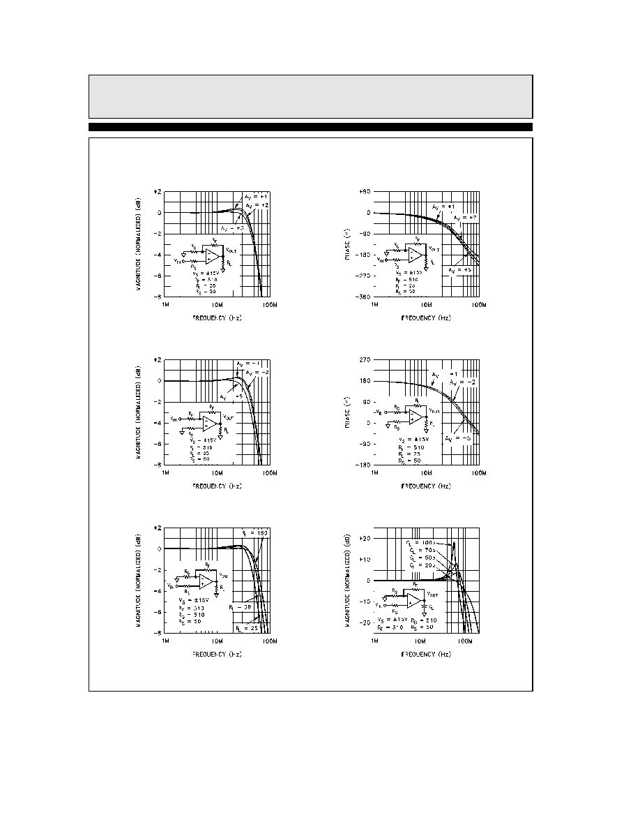
Typical Performance Curves
(T
A
e
25 C R
L
e
25
X A
V
e a
2 R
F
e
510 unless otherwise specified)
Frequency Response (GAIN)
Non-Inverting
Frequency Response (PHASE)
Non-Inverting
Response (GAIN)
Inverting Frequency
Response (PHASE)
Inverting Frequency
Frequency Response for Various R
L
Frequency Response for Various C
L
2099 ≠ 2
4
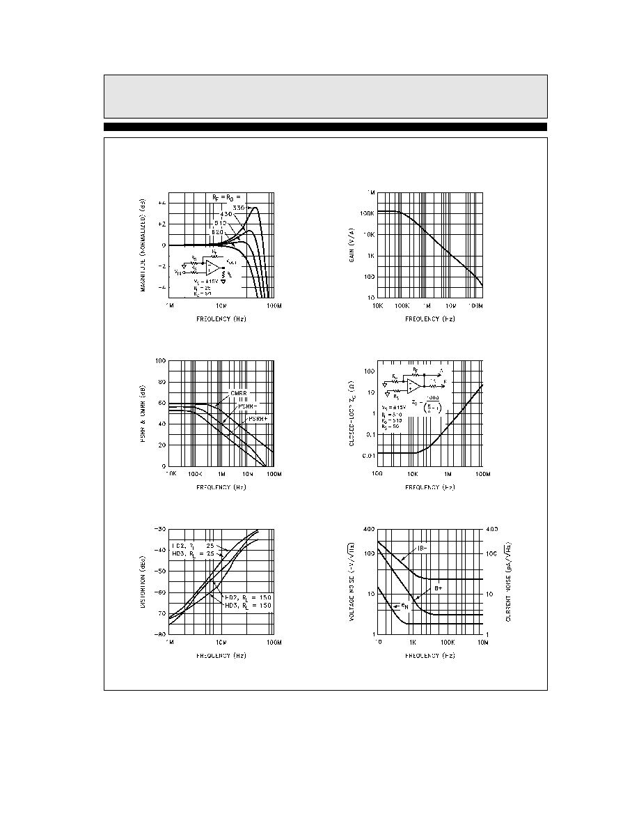
EL2099C
Video Distribution Amplifier
Typical Performance Curves
(T
A
e
25 C R
L
e
25
X A
V
e
a
2 R
F
e
510 unless otherwise specified)
Contd
Various R
F
R
G
Frequency Response for
Transimpedance (R
OL
)
PSRR
CMRR vs Frequency
Impedance vs Frequency
Closed-Loop Output
Distortion vs Frequency
2nd and 3rd Harmonic
Noise vs Frequency
Voltage and Current
2099 ≠ 3
5