 | –≠–ª–µ–∫—Ç—Ä–æ–Ω–Ω—ã–π –∫–æ–º–ø–æ–Ω–µ–Ω—Ç: EL2120C | –°–∫–∞—á–∞—Ç—å:  PDF PDF  ZIP ZIP |

EL2120C
January
1996
Rev
E
EL2120C
100 MHz Current Feedback Amplifier
Note All information contained in this data sheet has been carefully checked and is believed to be accurate as of the date of publication however this data sheet cannot be a ``controlled document'' Current revisions if any to these
specifications are maintained at the factory and are available upon your request We recommend checking the revision level before finalization of your design documentation
1991 Elantec Inc
Features
Excellent differential gain and
phase on
g
5V to
g
15V supplies
100 MHz
b
3 dB bandwidth from
gains of
g
1 to
g
10
700 V ms slew rate
0 1 dB flatness to 20 MHz
Output disable in 50 ns - remains
high impedance even when
driven with large slew rates
Single
a
5V supply operation
AC characteristics are lot and
temperature stable
Available in small SO-8 package
Applications
Video gain block
Residue amplifier
Multiplexer
Current to voltage converter
Coax cable driver with gain of 2
ADC driver
Ordering Information
Part No
Temp Range
Package
Outline
EL2120CN
0 C to
a
75 C
8-Pin P-DIP
MDP0031
EL2120CS
0 C to
a
75 C
8-Lead SO
MDP0027
Connection Diagrams
P-DIP
2120 ≠ 1
SO
2120 ≠ 2
Top View
General Description
The EL2120C is a wideband current feedback amplifier opti-
mized for video performance Its 0 01% differential gain and
0 03 degree differential phase performance when at
g
5V sup-
plies exceeds the performance of other amplifiers running on
g
15V supplies Operating on
g
8 to
g
15V supplies reduces dis-
tortions to 0 01% and 0 01 degrees and below The EL2120C can
operate with supplies as low as
g
2 5V or a single
a
5V supply
Being a current feedback design bandwidth is a relatively con-
stant 100 MHz over the
g
1 to
g
10 gain range The EL2120C
has been optimized for flat gain over frequency and all charac-
teristics are maintained at positive unity gain Because the in-
put slew rate is similar to the 700 V
ms output slew rate the
part makes an excellent high-speed buffer
The EL2120C has a superior output disable function Time to
enable or disable is 50 ns and does not change markedly with
temperature Furthermore in disable mode the output does not
draw excessive currents when driven with 1000 V
ms slew rates
The output appears as a 3 pF load when disabled
Simplified Schematic
2120 ≠ 21

EL2120C
100 MHz Current Feedback Amplifier
Absolute Maximum Ratings
(T
A
e
25 C)
Voltage between V
a
and V
b
33V
Voltage at
a
IN
b
IN V
OUT
(V
b
)
b
0 5V to (V
a
)
a
0 5V
Voltage between
a
IN and
b
IN
g
5V
Voltage at Disable
(V
a
)
b
10V to (V
a
)
a
0 5V
Current into
a
IN
b
IN and Disable
g
5 mA
Output Current
g
50 mA
Internal Power Dissipation
See Curves
Operating Ambient
Temperature Range
0 to 75 C
Operating Junction Temperature
P-DIP or SO
150 C
Storage Temperature Range
b
65 C to
a
150 C
Important Note
All parameters having Min Max specifications are guaranteed The Test Level column indicates the specific device testing actually
performed during production and Quality inspection Elantec performs most electrical tests using modern high-speed automatic test
equipment specifically the LTX77 Series system Unless otherwise noted all tests are pulsed tests therefore T
J
e
T
C
e
T
A
Test Level
Test Procedure
I
100% production tested and QA sample tested per QA test plan QCX0002
II
100% production tested at T
A
e
25 C and QA sample tested at T
A
e
25 C
T
MAX
and T
MIN
per QA test plan QCX0002
III
QA sample tested per QA test plan QCX0002
IV
Parameter is guaranteed (but not tested) by Design and Characterization Data
V
Parameter is typical value at T
A
e
25 C for information purposes only
Open Loop DC Electrical Characteristics
V
S
e
g
5V R
L
e
150
X T
A
e
25 C unless otherwise specified
Parameter
Description
Temp
Min
Typ
Max
Test
Units
Level
V
OS
Input Offset Voltage
Full
4
20
II
mV
V
S
e
g
15V
Full
2
25
II
mV
DV
OS
DT
Input Offset Drift
Full
20
V
mV C
I
Ba
a
V
IN
Input Bias Current
Full
5
15
II
mA
I
Bb
b
V
IN
Input Bias Current
Full
10
50
II
mA
CMRR
Common-Mode Rejection
Full
50
55
II
dB
(Note 1)
b
ICMR
b
Input Current Common-Mode
Full
8
20
II
mA V
Rejection (Note 1)
PSRR
Power Supply Rejection
Full
65
80
II
dB
(Note 2)
a
IPSR
a
Input Current Power Supply
25 C
0 03
V
mA V
Rejection (Note 2)
b
IPSR
b
Input Current Power Supply
Full
0 6
5
II
mA V
Rejection (Note 2)
R
OL
Transimpedance
Full
70
140
II
k
X
A
VOL
Voltage Gain
Full
58
66
II
dB
a
R
IN
a
V
IN
Input Impedance
25 C
2
V
M
X
2
TD
is
32in

EL2120C
100 MHz Current Feedback Amplifier
Open Loop DC Electrical Characteristics
Contd
V
S
e
g
5V R
L
e
150
X T
A
e
25 C unless otherwise specified
Parameter
Description
Temp
Min
Typ
Max
Test
Units
Level
V
IN
a
V
IN
Range
Full
g
3 0
g
3 5
II
V
V
O
Output Voltage Swing
Full
g
3 0
g
3 5
II
V
I
SC
Output Short-Circuit
25 C
100
II
mA
Current
I
O DIS
Output Current Disabled
Full
5
50
II
mA
V
DIS ON
Disable Pin Voltage for
Full
(V
a
)
b
1
II
V
Output Enabled
V
DIS OFF
Disable Pin Voltage for
Full
(V
a
)
b
4
II
V
Output Disabled
I
DIS ON
Disable Pin Current for
Full
5
II
mA
Output Enabled
I
DIS OFF
Disable Pin Current for
Full
1 0
II
mA
Output Disabled
I
S
Supply Current (V
S
e
g
15V)
Full
17
20
II
mA
Note 1 The input is moved from
b
3V to
a
3V
Note 2 The supplies are moved from
g
5V to
g
15V
Closed Loop AC Electrical Characteristics
V
S
e
g
15V A
V
e a
2 (R
F
e
R
G
e
270
X) R
L
e
150
X C
L
e
7 pF C
INb
e
2 pF T
A
e
25 C
Parameter
Description
Min
Typ
Max
Test
Units
Level
SR
Slew Rate V
OUT
from
b
3V to
a
3V
Measured at
b
2V and
a
2V
V
S
e
g
15V
750
V
V
ms
V
S
e
g
5V
550
V
V
ms
t
S
Settling Time to 0 25% of a
0 to
a
10V Swing A
V
e a
1 with
R
F
e
270
X R
G
e
%
and R
L
e
400
X
50
V
ns
BW
Bandwidth
b
3 dB
95
V
MHz
g
1 dB
50
V
MHz
g
0 1 dB
16
V
MHz
BW 2 5V
Bandwidth at
b
3 dB
75
V
MHz
V
S
e
g
2 5V
g
1 dB
35
V
MHz
g
0 1 dB
11
V
MHz
Peaking
0 5
V
dB
3
TD
is
27in
TD
is
24in
EL2120C
100 MHz Current Feedback Amplifier
Closed Loop AC Electrical Characteristics
Contd
V
S
e
g
15V A
V
e a
2 (R
F
e
R
G
e
270
X) R
L
e
150
X C
L
e
7 pF C
INb
e
2 pF T
A
e
25 C
Parameter
Description
Min
Typ
Max
Test
Units
Level
dG
Differential Gain DC Offset
from
b
0 7V through
a
0 7V AC
Amplitude 286 mVp ≠ p
V
S
e
g
15V f
e
3 58 MHz
k
0 01
V
%
V
S
e
g
15V f
e
30 MHz
0 1
V
%
V
S
e
g
5V f
e
3 58 MHz
0 01
V
%
d
i
Differential Phase DC Offset
from
b
0 7V through
a
0 7V AC
Amplitude 286 mVp ≠ p
V
S
e
g
15V f
e
3 58 MHz
0 01
V
V
S
e
g
15V f
e
30 MHz
0 1
V
V
S
e
g
5V f
e
3 58 MHz
0 06
V
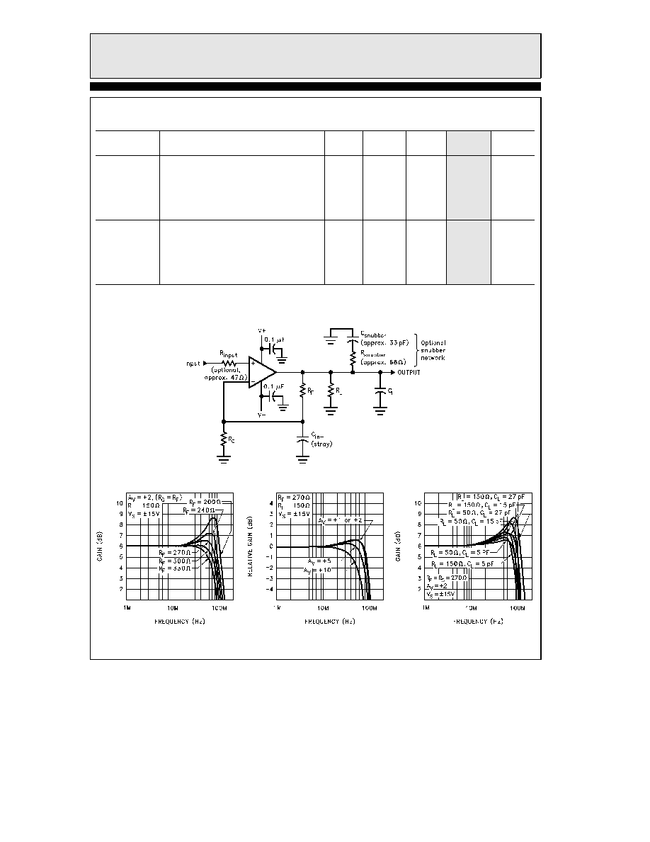
Typical Performance Curves
AC Test Circuit
2120 ≠ 3
Frequency Response vs R
F
2120 ≠ 4
Frequency Response vs Gain
2120 ≠ 5
Frequency Response vs Load
2120 ≠ 6
4
TD
is
20in
EL2120C
100 MHz Current Feedback Amplifier
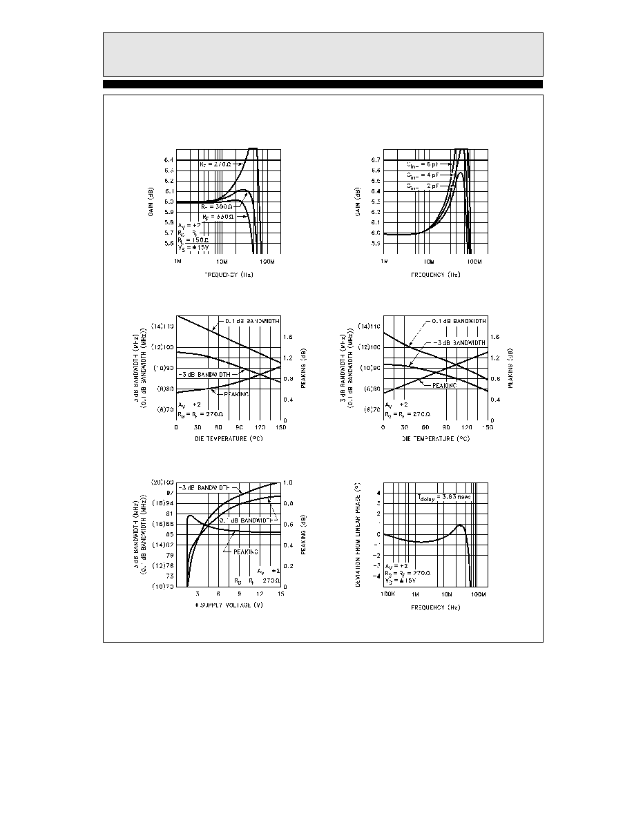
Typical Performance Curves
Contd
Gain Flatness vs R
F
Gain Flatness vs C
IN
b
at V
S
g
15V
and Peaking vs Temperature
b
3 dB Bandwidth 0 1 dB Bandwidth
at V
S
g
5V
and Peaking vs Temperature
b
3 dB Bandwidth 0 1 dB Bandwidth
Peaking vs Supply Voltage
0 1 dB Bandwidth and
b
3 dB Bandwidth
Phase vs Frequency
Deviation From Linear
2120 ≠ 7
5

EL2120C
100 MHz Current Feedback Amplifier
Typical Performance Curves
Contd
at 3 58 MHz
DC Input Offset
Differential Gain vs
at 3 58 MHz
DC Input Offset
Differential Phase vs
at 30 MHz
DC Input Offset
Differential Gain vs
at 30 MHz
DC Input Offset
Differential Phase vs
(V
IN
DC from 0 to a0 7V)
vs Supply Voltage
Differential Gain and Phase
and Current
Input Noise Voltage
2120 ≠ 8
6

EL2120C
100 MHz Current Feedback Amplifier
Typical Performance Curves
Contd
Swing vs Frequency
Undistorted Output
Slew Rate vs Temperature
2120 ≠ 9
Small-Signal Transient Response
2120 ≠ 10
A
V
e a
2 R
F
e
R
G
e
270
X
R
L
e
150
X
Large-Signal Transient Response
2120 ≠ 11
A
V
e a
2 R
F
e
R
G
e
270
X
R
L
e
150
X V
S
e
g
15V
Settling Time vs Swing
Long Term Settling Error
2120 ≠ 12
7

EL2120C
100 MHz Current Feedback Amplifier
Typical Performance Curves
Contd
Enable Response for
a Family of Inputs
2120 ≠ 13
A
V
e a
2 R
L
e
150
X
V
S
e
g
5V
Disable Response for
a Family of Inputs
A
V
e a
2 R
L
e
150
X
2120 ≠ 14
V
S
e
g
5V
Supply Voltage
Supply Current vs
Maximum Power Dissipation
8-Pin Plastic DIP
vs Ambient Temperature
8-Lead SO
vs Ambient Temperature
Maximum Power Dissipation
2120 ≠ 15
8

EL2120C
100 MHz Current Feedback Amplifier
Applications Information
The EL2120C represents the third generation of
current-feedback amplifier design It is designed
to provide good high-frequency performance over
wide supply voltage load impedance gain tem-
perature and manufacturing lot variations It is
a well-behaved amplifier in spite of its 100 MHz
bandwidth but a few precautions should be tak-
en to obtain maximum performance
The power supply pins must be well bypassed
0 01
mF ceramic capacitors are adequate but lead
length should be kept below
and a ground
plane is recommended Bypassing with 4 7
mF
tantalum capacitors can improve settling charac-
teristics and smaller capacitors in parallel will
not be needed The lead length of sockets general-
ly deteriorates the amplifier's frequency response
by exaggerating peaking and increasing ringing
in response to transients Short sockets cause lit-
tle degradation
Load capacitance also increases ringing and
peaking Capacitance greater than 35 pF should
be isolated with a series resistor Capacitance at
the V
IN
b
terminal has a similar effect
and
should be kept below 5 pF Often the inductance
of the leads of a load capacitance will be self-reso-
nant at frequencies from 40 MHz to 200 MHz
and can cause oscillations A resonant load can be
de-Q'ed with a small series or parallel resistor A
``snubber'' can sometimes be used to reduce reso-
nances This is a resistor and capacitor in series
connected from output to ground Values of 68
X
and 33 pF are typical Increasing the feedback
resistor can also improve frequency flatness
The V
IN
a
pin can oscillate in the 200 MHz to
500 MHz realm if presented with a resonant or
inductive source impedance A series 27
X to 68X
resistor right on the V
IN
a
pin will suppress such
oscillations without affecting frequency response
b
3 dB bandwidth is inversely proportional to
the value of feedback resistor R
F
The EL2120C
will tolerate values as low as 180
X for a maxi-
mum bandwidth of about 140 MHz but peaking
will increase and tolerance to stray capacitance
will reduce At gains greater than 5
b
3 dB band-
width begins to reduce and a smaller R
F
can be
used to maximize frequency response
The greatest frequency response flatness (to
0 1 dB for instance) occurs with R
F
e
300
X to
330
X Even the moderate peaking caused by low-
er values of R
F
will cause the gain to peak out of
the 0 1 dB window and higher values of R
F
will
cause an overcompensated response where the
gain falls below the 0 1 dB level Parasitic capaci-
tances will generally degrade the frequency flat-
ness
The EL2120C should not output a continuous
current above 50 mA as stated in the ABSO-
LUTE MAXIMUM RATINGS table The out-
put current limit is set to 120 mA at a die temper-
ature of 25 C and reduces to 85 mA at a die tem-
perature of 150 C This large current is needed to
slew load capacitance and drive low impedance
loads with low distortion but cannot be support-
ed continuously Furthermore package dissipa-
tion capabilities cannot be met under short-cir-
cuit conditions Current limit should not occur
longer than a few seconds
The output disable function of the EL2120C is
optimized for video performance While in dis-
able mode the feedthrough of the circuit can be
modeled as a 0 2 pF capacitor from V
IN
a
to the
output No more than
g
5V can be placed be-
tween V
IN
a
and V
IN
b
in disable mode but this
is compatible with common video signal levels
In disabled state the output can withstand about
1000 V
ms slew rate signals impressed on it with-
out the output transistors turning on
The
Disable pin logic level is referred to V
a
With
g
5V supplies a CMOS or TTL driver with
pull-up resistor will suffice
g
15V supplies re-
quire a
a
14
a
11V drive span or
a
15
a
10V
nominally
Open-collector TTL with a tapped
pull-up resistor can provide these spans The im-
pedance of the divider should be 1k or less for
optimum enable disable speed
The EL2120C enables in 50 ns or less When V
IN
e
0 only a small switching glitch occurs at the
output When V
IN
is some other value the out-
put overshoots by about 0 7V when settling
toward its new enabled value
9
EL2120C
100 MHz Current Feedback Amplifier
Applications Information
Contd
When the EL2120C disables it turns off very rapidly for inputs of
g
1V or less and the output sags
more slowly for inputs larger than this For inputs as large as
g
2 5V the output current can be
absorbed by another EL2120C simultaneously enabled Under these conditions switching will be prop-
erly completed in 50 ns or less
The greater thermal resistance of the SO-8 package requires that the EL2120C be operated from
g
10V
supplies or less to maintain the 150 C maximum die temperature over the commercial temperature
range The P-DIP package allows the full
g
16 5V supply operation
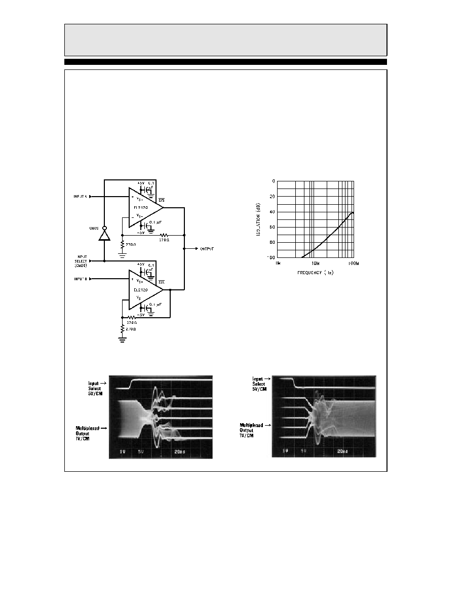
Typical Applications Circuit
A High Quality Two-Input Multiplexer
Dual EL2120C Multiplexer
2120 ≠ 16
Channel-to-Channel Isolation
of Dual EL2120C Multiplexer
2120 ≠ 17
Dual EL2120C Multiplexer Switching
Channels Uncorrelated Sinewave
Switched to a Family of DC Levels
2120 ≠ 18
Dual EL2120C Multiplexer Switching
Channels a Family of DC Levels
Switched to an Uncorrelated Sinewave
2120 ≠ 19
10

EL2120C
100 MHz Current Feedback Amplifier
The EL2120C Macromodel
This macromodel has been developed to assist the user in simulating the EL2120C with surrounding
circuitry It was developed for the PSPICE simulator (copywritten by the Microsim corporation) and
may need to be rearranged for other simulators particularly the H operator It approximates frequency
response and small-signal transients as well although the effects of load capacitance does not show
This model is slightly more complicated than the models used for low-frequency op-amps but is much
more accurate for AC
The model does not simulate these characteristics accurately
noise
non-linearities
slew rate limitations
temperature effects
settling time
manufacturing variations
input or output resonances CMRR and PSRR
Revision A March 1992
Enhancements include PSRR CMRR and Slew Rate Limiting
Connections
a
input
l
b
input
l
l
a
Vsupply
l
l
l
b
Vsupply
l
l
l
l
output
l
l
l
l
l
subckt M2120
3
2
7
4
6
Input Stage
q1 4 18 19 qp
e1 10 0 3 0 1 0
q2 7 18 20 qn
vis 10 9 0V
q3 7 19 21 qn
h2 9 12 vxx 1 0
q4 4 20 22 qp
r1 2 11 25
r7 21 6 4
l1 11 12 20nH
r8 22 6 4
iinp 3 0 10
mA
ios1 7 19 2 5mA
iinm 2 0 5
mA
ios2 20 4 2 5mA
r12 3 0 2Meg
Supply
Slew Rate Limiting
ips 7 4 10mA
h1 13 0 vis 600
r2 13 14 1K
Error Terms
d1 14 0 dclamp
s2 0 14 dclamp
ivos 0 23 5mA
vxx 23 0 0V
High Frequency Pole
e4 24 0 6 0 1 0
e5 25 0 7 0 1 0
e2 30 0 14 0 0 00166666666
e6 26 0 4 0 1 0
15 30 17 1
mH
r9 24 23 562
c5 17 0 0 5pF
r10 25 23 10K
r5 17 0 600
r11 26 23 10K
Transimpedance Stage
Models
g1 0 18 17 0 1 0
model qn npn (is
e
5e
b
15 bf
e
500 tf
e
0 1nS)
rol 18 0 140K
model qp pnp (is
e
5e
b
15 bf
e
500 tf
e
0 1nS)
cdp 18 0 7 9pF
model dclamp d(is
e
1e
b
30 ibv
e
0 02 bv
e
4 n
e
4)
ends
Output Stage
11
TAB
WIDE
TD
is
38in
TD

EL2120C
January
1996
Rev
E
EL2120C
100 MHz Current Feedback Amplifier
The EL2120C Macromodel
Contd
2120 ≠ 20
EL2120 Macromodel
General Disclaimer
Specifications contained in this data sheet are in effect as of the publication date shown Elantec Inc reserves the right to make changes
in the circuitry or specifications contained herein at any time without notice Elantec Inc assumes no responsibility for the use of any
circuits described herein and makes no representations that they are free from patent infringement
Elantec Inc
1996 Tarob Court
Milpitas CA 95035
Telephone (408) 945-1323
(800) 333-6314
Fax (408) 945-9305
European Office 44-71-482-4596
WARNING
Life Support Policy
Elantec Inc products are not authorized for and should not be
used within Life Support Systems without the specific written
consent of Elantec Inc Life Support systems are equipment in-
tended to support or sustain life and whose failure to perform
when properly used in accordance with instructions provided can
be reasonably expected to result in significant personal injury or
death Users contemplating application of Elantec Inc products
in Life Support Systems are requested to contact Elantec Inc
factory headquarters to establish suitable terms
conditions for
these applications Elantec Inc 's warranty is limited to replace-
ment of defective components and does not cover injury to per-
sons or property or other consequential damages
Printed in U S A
12