 | –≠–ª–µ–∫—Ç—Ä–æ–Ω–Ω—ã–π –∫–æ–º–ø–æ–Ω–µ–Ω—Ç: EL2125CW | –°–∫–∞—á–∞—Ç—å:  PDF PDF  ZIP ZIP |
Note: All information contained in this data sheet has been carefully checked and is believed to be accurate as of the date of publication; however, this data sheet cannot be a "controlled document". Current revisions, if any, to these
specifications are maintained at the factory and are available upon your request. We recommend checking the revision level before finalization of your design documentation.
© 2001 Elantec Semiconductor, Inc.
E
L
2
1
2
5
C
-
P
r
e
l
i
m
i
n
a
r
y
Features
∑ Voltage noise of only 0.83nV/
Hz
∑ Current noise of only 2.4pA/
Hz
∑ Low offset voltage
200µV
∑ 180MHz -3dB BW for A
V
=10
∑ Low supply current - 10mA
∑ SOT23 package available
∑ ±2.5V to ±15V operation
Applications
∑ Ultrasound input amplifiers
∑ Wideband instrumentation
∑ Communication equipment
∑ AGC & PLL active filters
∑ Wideband sensors
Ordering Information
Part No
Package
Tape & Reel
Outline #
EL2125CW
5-Pin SOT23
MDP0038
EL2125CS
8-Pin SO
MDP0027
EL2125CN
8-Pin PDIP
MDP0031
General Description
The EL2125C is an ultra-low noise, wideband amplifier that runs on
half the supply current of competitive parts. It is intended for use in
systems such as ultrasound imaging where a very small signal needs to
be amplified by a large amount without adding significant noise. Its
low power dissipation enables it to be packaged in the tiny SOT23
package, which further helps systems where many input channels cre-
ate both space and power dissipation problems.
The EL2125C is stable for gains of 10 and greater and uses traditional
voltage feedback. This allows the use of reactive elements in the feed-
back loop, a common requirement for many filter topologies. It
operates from ±2.5V to ±15V supplies and is available in a 5-pin
SOT23 package and 8-pin SO and 8-pin PDIP packages.
The EL2125C is fabricated in Elantec's proprietary complementary
bipolar process, and is specified for operation from -45∞C to +85∞C.
Connection Diagrams
1
2
3
4
8
7
6
5
EL2125CS
(8-Pin SO and 8-Pin PDIP)
1
2
3
5
4
EL2125CW
(5-Pin SOT23)
-
+
-
+
VS+
IN-
IN+
VS-
OUT
NC
IN-
IN+
VS-
NC
VS+
OUT
NC
EL2125C - Preliminary
Ultra-low Noise, Low Power, Wideband Amplifier
O
c
t
o
b
e
r
2
,
2
0
0
1
2
EL2125C - Preliminary
Ultra-low Noise, Low Power, Wideband Amplifier
E
L
2
1
2
5
C
-
P
r
e
l
i
m
i
n
a
r
y
Absolute Maximum Ratings
(T
A
= 25∞C)
V
S
+ to V
S
-
33V
Continuous Output Current
40mA
Any Input
V
S
- - 0.3V to V
S
+ + 0.3V
Power Dissipation
See Curves
Operating Temperature
-45∞C to +85∞C
Storage Temperature
-60∞C to +150∞C
Important Note:
All parameters having Min/Max specifications are guaranteed. Typ values are for information purposes only. Unless otherwise noted, all tests are at the
specified temperature and are pulsed tests, therefore: T
J
= T
C
= T
A
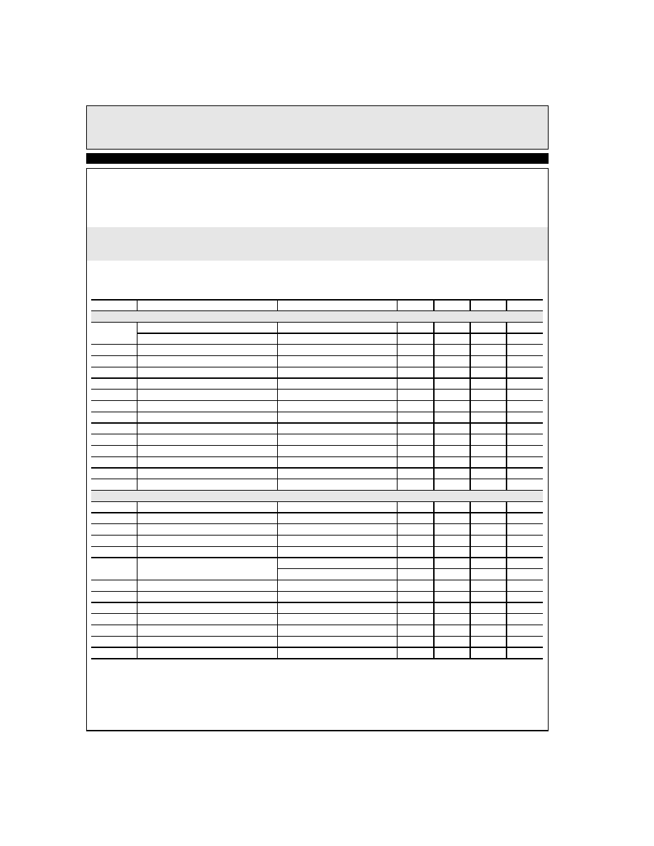
Electrical Characteristics
V
S
= ±5V, T
A
= 25∞C, R
F
= 180
, R
G
= 20
, R
L
= 500
unless otherwise specified.
Parameter
Description
Conditions
Min
Typ
Max
Unit
DC Performance
V
OS
Input Offset Voltage (SO8 & PDIP8)
-0.2
2
mV
Input Offset Voltage (SOT23-5)
3
mV
T
CVOS
Offset Voltage Temperature Coefficient
TBD
µV/∞C
I
B
Input Bias Current
-30
-21
µA
I
OS
Input Bias Current Offset
0.2
1
µA
T
CIB
Input Bias Current Temperature Coefficient
TBD
nA/∞C
C
IN
Input Capacitance
2.2
pF
A
VOL
Open Loop Gain
65
81
dB
PSRR
Power Supply Rejection Ratio
[1]
75
96
dB
CMRR
Common Mode Rejection Ratio
[2]
65
100
dB
CMIR
Common Mode Input Range
V
V
OUT
Output Voltage Swing
No load, R
F
= 1k
3.5
3.8
V
V
OUTL
Output Voltage Swing
R
L
= 100
2.8
3.1
V
I
OUT
Output Short Circuit Current
[3]
80
100
mA
I
S
Supply Current
10.1
12
mA
AC Performance - R
G
= 20
, C
L
= 5pF
BW
-3dB Bandwidth
175
MHz
BW ±0.1dB
±0.1dB Bandwidth
34
MHz
BW ±1dB
±1dB Bandwidth
150
MHz
Peaking
Peaking
0.4
dB
SR
Slew Rate
V
OUT
= 2V
PP
, measured at 20% to 80%
TBD
190
V/µs
OS
Overshoot, 4Vpk-pk Output Square Wave
Positive
0.6
%
Negative
2.7
%
T
S
Settling Time to 0.1% of ±1V Pulse
TBD
ns
V
N
Voltage Noise Spectral Density
0.83
nV/
Hz
I
N
Current Noise Spectral Density
2.4
pA/
Hz
HD2
2nd Harmonic Distortion
[4]
TBD
dBc
HD3
3rd Harmonic Distortion
[4]
TBD
dBc
THD
Total Harmonic Distortion
[5]
TBD
dBc
IMD
Intermodulation Distortion
[6]
TBD
%
1. Measured by moving the supplies from ±4V to ±6V
2. Measured by moving the inputs from +3.5V to -4.4V
3. Pulse test only
4. Frequency = 10MHz, V
OUT
= 1Vpk-pk, into 100
and 5pF load
5. Frequency = 20MHz, V
OUT
= -20dBm (0.0274V
RMS
) into 500
and 15pF load
6. Two-tone IMD, frequencies = 5MHz and 6MHz at -20dBm output level, R
LOAD
= 500
and 15pF
3
EL2125C - Preliminary
Ultra-low Noise, Low Power, Wideband Amplifier
E
L
2
1
2
5
C
-
P
r
e
l
i
m
i
n
a
r
y
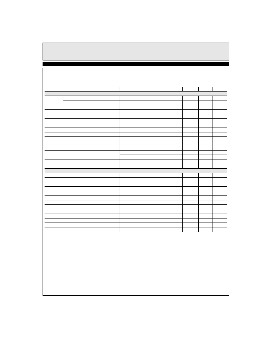
Electrical Characteristics
V
S
= ±15V, T
A
= 25∞C, R
F
= 180
, R
G
= 20
, R
L
= 500
unless otherwise specified.
Parameter
Description
Conditions
Min
Typ
Max
Unit
DC Performance
V
OS
Input Offset Voltage (SO8 & PDIP8)
-0.2
2
mV
Input Offset Voltage (SOT23-5)
3
mV
T
CVOS
Offset Voltage Temperature Coefficient
TBD
µV/∞C
I
B
Input Bias Current
-30
-21
µA
I
OS
Input Bias Current Offset
0.16
1
µA
T
CIB
Input Bias Current Temperature Coefficient
TBD
nA/∞C
C
IN
Input Capacitance
2.2
pF
A
VOL
Open Loop Gain
75
86
dB
PSRR
Power Supply Rejection Ratio
[1]
75
95
dB
CMRR
Common Mode Rejection Ratio
[2]
75
100
dB
CMIR
Common Mode Input Range
TBD
V
V
OUT
Output Voltage Swing
No load, R
F
= 1k
13.5
V
V
OUTL
Output Voltage Swing
Positive, R
F
= 180
, R
L
= 500
12.1
V
Negative
-11.3
V
I
OUT
Output Short Circuit Current
[3]
100
150
mA
I
S
Supply Current
10.8
12
mA
AC Performance - R
G
= 20
, C
L
= 5pF
BW
-3dB Bandwidth
220
MHz
BW ±0.1dB
±0.1dB Bandwidth
23
MHz
BW ±1dB
±1dB Bandwidth
63
MHz
Peaking
Peaking
2.5
dB
SR
Slew Rate
V
OUT
= 2V
PP
, measured at 20% to 80%
TBD
225
V/µs
OS
Overshoot, 4Vpk-pk Output Square Wave
0.6
%
T
S
Settling Time to 0.1% of ±1V Pulse
TBD
ns
V
N
Voltage Noise Spectral Density
0.95
nV/
Hz
I
N
Current Noise Spectral Density
2.1
pA/
Hz
HD2
2nd Harmonic Distortion
[4]
TBD
dBc
HD3
3rd Harmonic Distortion
[4]
TBD
dBc
THD
Total Harmonic Distortion
[5]
TBD
dBc
IMD
Intermodulation Distortion
[6]
TBD
%
1. Measured by moving the supplies from ±13.5V to ±16.5V
2. Measured by moving the inputs from +13.5V to -14.4V
3. Pulse test only
4. Frequency = 10MHz, V
OUT
= 1Vpk-pk, into 100
and 5pF load
5. Frequency = 20MHz, V
OUT
= -20dBm (0.0274V
RMS
) into 500
and 15pF load
6. Two-tone IMD, frequencies = 5MHz and 6MHz at -20dBm output level, R
LOAD
= 500
and 15pF
4
EL2125C - Preliminary
Ultra-low Noise, Low Power, Wideband Amplifier
E
L
2
1
2
5
C
-
P
r
e
l
i
m
i
n
a
r
y
Typical Performance Curves
Non-Inverting Frequency Response for Various R
F
5
-5
1M
10M
100M
1G
Frequency (Hz)
N
o
r
m
a
l
i
z
e
d
G
a
i
n
(
d
B
)
Inverting Frequency Response for Various R
F
6
2
-2
-6
-10
-14
1M
10M
100M
1G
Frequency (Hz)
N
o
r
m
a
l
i
z
e
d
G
a
i
n
(
d
B
)
Inverting Frequency Response for Various R
F
6
2
-2
-6
-10
-14
1M
10M
100M
1G
Frequency (Hz)
N
o
r
m
a
l
i
z
e
d
G
a
i
n
(
d
B
)
Non-Inverting Frequency Response for Various R
F
5
0
-5
1M
10M
100M
1G
Frequency (Hz)
N
o
r
m
a
l
i
z
e
d
G
a
i
n
(
d
B
)
0
R
F
=1k
R
F
=499
R
F
=180
R
F
=100
R
F
=1k
R
F
=180
R
F
=700
R
F
=100
R
F
=499
V
S
=±5V
A
V
=-10
C
L
=5pF
R
F
=1k
R
F
=350
R
F
=200
R
F
=97.6
R
F
=499
V
S
=±15V
A
V
=-10
C
L
=5pF
R
F
=1k
R
F
=350
R
F
=200
R
F
=499
R
F
=97.6
V
S
=±5V
A
V
=10
R
L
=500
C
L
=5pF
V
S
=±15V
A
V
=10
R
L
=500
C
L
=5pF
-5
0
5
1M
10M
100M
1G
Frequency (Hz)
N
o
r
m
a
l
i
z
e
d
G
a
i
n
(
d
B
)
Non-Inverting Frequency Response vs Gain
V
S
=±5V
R
L
=500
C
L
=5pF
R
G
=20
-5
0
5
N
o
r
m
a
l
i
z
e
d
G
a
i
n
(
d
B
)
Non-Inverting Frequency Response for Various Gain
A
V
=10
A
V
=20
A
V
=50
V
S
=±15V
R
L
=500
C
L
=5pF
R
F
=700
1M
10M
100M
1G
Frequency (Hz)
A
V
=10
A
V
=20
A
V
=50
5
EL2125C - Preliminary
Ultra-low Noise, Low Power, Wideband Amplifier
E
L
2
1
2
5
C
-
P
r
e
l
i
m
i
n
a
r
y
Typical Performance Curves
6
N
o
r
m
a
l
i
z
e
d
G
a
i
n
(
d
B
)
Inverting Frequency Response vs Gain
2
-2
-6
-10
-14
0
6
N
o
r
m
a
l
i
z
e
d
G
a
i
n
(
d
B
)
Inverting Frequency Response vs Gain
1M
10M
100M
1G
Frequency (Hz)
-14
A
V
=-10
R
F
=350k
A
V
=-50
R
F
=1.75k
A
V
=-20
R
F
=700k
V
S
=±5V
R
L
=500
C
L
=5pF
1M
10M
100M
1G
Frequency (Hz)
A
V
=-50
A
V
=-20
A
V
=-10
V
S
=±15V
R
L
=500
C
L
=5pF
R
G
=50
-5
5
N
o
r
m
a
l
i
z
e
d
G
a
i
n
(
d
B
)
Non-Inverting Frequency Response for Various Output
Signal Levels
0
-14
6
N
o
r
m
a
l
i
z
e
d
G
a
i
n
(
d
B
)
Inverting Frequency Response for Various Output Signal
Levels
0
1M
10M
100M
1G
Frequency (Hz)
V
S
=±5V
A
V
=10
R
F
=180
R
L
= 500
C
L
=5pF
1V
PP
2V
PP
4V
PP
30mV
PP
500mV
PP
1V
PP
1M
10M
100M
1G
Frequency (Hz)
V
S
=±5V
A
V
=-10
R
F
=350
R
L
= 500
C
L
=5pF
2.5V
PP
500mV
PP
3.3V
PP
250mV
PP
1V
PP
3mV
PP
5
N
o
r
m
a
l
i
z
e
d
G
a
i
n
(
d
B
)
Non-Inverting Frequency Response for Various C
L
3
1
-1
-3
0
5
N
o
r
m
a
l
i
z
e
d
G
a
i
n
(
d
B
)
Non-Inverting Frequency Response for Various C
L
-5
1M
10M
100M
1G
Frequency (Hz)
V
S
=±5V
A
V
=10
R
F
=180
R
L
=500
C
L
=28.5pF
C
L
=16pF
C
L
=5pF
C
L
=1pF
-5
1M
10M
100M
1G
Frequency (Hz)
V
S
=±5V
A
V
=10
R
F
=700
R
L
=500
C
L
=17pF
C
L
=11pF
C
L
=1.2pF
C
L
=5pF

6
EL2125C - Preliminary
Ultra-low Noise, Low Power, Wideband Amplifier
E
L
2
1
2
5
C
-
P
r
e
l
i
m
i
n
a
r
y
Typical Performance Curves
6
N
o
r
m
a
l
i
z
e
d
G
a
i
n
(
d
B
)
Inverting Frequency Response for Various C
L
0
6
N
o
r
m
a
l
i
z
e
d
G
a
i
n
(
d
B
)
Inverting Frequency Response for Various C
L
2
-2
-6
-10
1M
10M
100M
1G
Frequency (Hz)
-14
C
L
=29.4pF
C
L
=16.4pF
C
L
=11.4pF
C
L
=5.1pF
C
L
=1.2pF
V
S
=±5V
A
V
=10
R
F
=350
R
L
=500
-14
1M
10M
100M
1G
Frequency (Hz)
C
L
=29.4pF
C
L
=16.4pF
C
L
=11.4pF
C
L
=5.1pF
C
L
=1.2pF
V
S
=±15V
A
V
=10
R
F
=500
R
L
=500
O
p
e
n
L
o
o
p
G
a
i
n
(
d
B
)
0
40
20
10k
Open Loop Gain and Phase
10M
60
80
100
100k
100M
Frequency (Hz)
1M
P
h
a
s
e
(
∞
)
-250
-50
-150
50
150
250
0
0
Supply Voltage (±V)
S
u
p
p
l
y
C
u
r
r
e
n
t
(
m
A
)
Supply Current vs Supply Voltage
4.8
12
2.4
3
12
15
9.6
7.2
6
9
Peaking vs Supply Voltage
3
2.5
2
1.5
1
0.5
0
2
4
6
8
10
12
14
16
V
S
(±V)
P
e
a
k
i
n
g
(
d
B
)
A
V
=10
A
V
=-10
A
V
=50
A
V
=-50
A
V
=20
A
V
=-20
3dB Bandwidth vs Supply Voltage
250
200
150
100
50
0
2
4
6
8
10
12
14
16
V
S
(±V)
B
a
n
d
w
i
d
t
h
(
M
H
z
)
A
V
=10
A
V
=-10
A
V
=50
A
V
=-50
A
V
=20
A
V
=-20
400M
7
EL2125C - Preliminary
Ultra-low Noise, Low Power, Wideband Amplifier
E
L
2
1
2
5
C
-
P
r
e
l
i
m
i
n
a
r
y
Typical Performance Curves
10ns/div
2
0
m
V
/
d
i
v
Small Signal Step Response
Small Signal Step Response
V
IN
x2
V
O
V
S
=±5V
R
L
=500
R
F
=180
A
V
=10
C
L
=5pF
10ns/div
2
0
m
V
/
d
i
v
V
IN
x2
V
O
V
S
=±15V
R
L
=500
R
F
=180
A
V
=10
C
L
=5pF
Time (20ns/div)
O
u
t
p
u
t
V
o
l
t
a
g
e
(
0
.
5
V
/
d
i
v
)
Large-Signal Step Response
V
S
=±5V
R
L
=500
R
F
=180
A
V
=10
C
L
=5pF
Time (20ns/div)
O
u
t
p
u
t
V
o
l
t
a
g
e
(
0
.
5
V
/
d
i
v
)
Large-Signal Step Response
V
S
=±15V
R
L
=500
R
F
=180
A
V
=10
C
L
=5pF
1MHz Harmonic Distortion vs Output Swing
-40
-50
-60
-70
-90
-100
-110
0
6
7
V
OUT
(V
PP
)
D
i
s
t
o
r
t
i
o
n
(
d
B
c
)
1MHz Harmonic Distortion vs Output Swing
-30
-40
-60
-80
-90
-100
-110
0
5
25
V
OUT
(V
PP
)
D
i
s
t
o
r
t
i
o
n
(
d
B
c
)
4
5
2
3
1
-80
V
S
=±5V
R
F
=180
A
V
=10
R
L
=500
2nd H
3rd H
V
S
=±15V
R
F
=180
A
V
=10
R
L
=500
10
15
20
-50
-70
2nd H
3rd H

8
EL2125C - Preliminary
Ultra-low Noise, Low Power, Wideband Amplifier
E
L
2
1
2
5
C
-
P
r
e
l
i
m
i
n
a
r
y
Typical Performance Curves
Voltage and Current Noise vs Frequency
100
10
1
0.1
10
100
1k
10k
100k
Frequency (Hz)
V
o
l
t
a
g
e
N
o
i
s
e
(
n
V
/
H
z
)
,
C
u
r
r
e
n
t
N
o
i
s
e
(
p
A
/
H
z
)
V
N
, V
S
=±15V
I
N
, V
S
=±5V
I
N
, V
S
=±15V
V
N
, V
S
=±5V
Settling Time vs Accuracy
60
50
40
30
20
10
0
0.1
1
10
Accuracy (%)
S
e
t
t
l
i
n
g
T
i
m
e
(
n
s
)
V
S
=±15V
V
O
=5V
PP
V
S
=±5V
V
O
=5V
PP
V
S
=±15V
V
O
=2V
PP
V
S
=±5V
V
O
=2V
PP
Total Harmonic Distortion vs Frequency
-30
-60
-80
-90
1k
10k
100M
Frequency (Hz)
T
H
D
(
d
B
c
)
V
S
=±5V
V
O
=2V
PP
A
V
=10
R
F
=180
R
L
=500
100k
1M
10M
-40
-50
-70
-6
14
1
400
Frequency (MHz)
G
r
o
u
p
D
e
l
a
y
(
n
s
)
Group Delay
2
10
6
-2
10
100
A
V
=20
A
V
=10
V
S
=±15V
-110
-10
10
100M
Frequency (Hz)
C
M
R
R
(
d
B
)
CMRR
-70
-30
-50
-99
100
10M
1k
10k
100k
1M
P
S
R
R
(
d
B
)
10
50
30
10K
PSRR
10M
70
90
110
100K
100M
Frequency (Hz)
1M
PSRR-
PSRR+
600M

9
EL2125C - Preliminary
Ultra-low Noise, Low Power, Wideband Amplifier
E
L
2
1
2
5
C
-
P
r
e
l
i
m
i
n
a
r
y
Typical Performance Curves
Bandwidth vs Temperature
200
160
40
0
-40
160
Temperature (∞C)
-
3
d
B
B
a
n
d
w
i
d
t
h
(
M
H
z
)
120
80
80
0
40
120
3.5
3
2.5
1.5
2
1
0.5
0
P
e
a
k
i
n
g
(
d
B
)
Bandwidth
Peaking
R
o
u
t
(
æ
)
0.001
0.1
0.01
10k
Closed Loop Output Impedance vs Frequency
1
10
100
Frequency (Hz)
100M
100k
1M
10M

10
EL2125C - Preliminary
Ultra-low Noise, Low Power, Wideband Amplifier
E
L
2
1
2
5
C
-
P
r
e
l
i
m
i
n
a
r
y
General Disclaimer
Specifications contained in this data sheet are in effect as of the publication date shown. Elantec, Inc. reserves the right to make changes in the cir-
cuitry or specifications contained herein at any time without notice. Elantec, Inc. assumes no responsibility for the use of any circuits described
herein and makes no representations that they are free from patent infringement.
WARNING - Life Support Policy
Elantec, Inc. products are not authorized for and should not be used
within Life Support Systems without the specific written consent of
Elantec, Inc. Life Support systems are equipment intended to sup-
port or sustain life and whose failure to perform when properly used
in accordance with instructions provided can be reasonably
expected to result in significant personal injury or death. Users con-
templating application of Elantec, Inc. Products in Life Support
Systems are requested to contact Elantec, Inc. factory headquarters
to establish suitable terms & conditions for these applications. Elan-
tec, Inc.'s warranty is limited to replacement of defective
components and does not cover injury to persons or property or
other consequential damages.
O
c
t
o
b
e
r
2
,
2
0
0
1
Printed in U.S.A.
Elantec Semiconductor, Inc.
675 Trade Zone Blvd.
Milpitas, CA 95035
Telephone: (408) 945-1323
(888) ELANTEC
Fax:
(408) 945-9305
European Office: +44-118-977-6020
Japan Technical Center: +81-45-682-5820