
Note: All information contained in this data sheet has been carefully checked and is believed to be accurate as of the date of publication; however, this data sheet cannot be a "controlled document". Current revisions, if any, to these
specifications are maintained at the factory and are available upon your request. We recommend checking the revision level before finalization of your design documentation.
© 2002 Elantec Semiconductor, Inc.
E
L
2126C
Features
∑ Voltage noise of only 1.3nV/
Hz
∑ Current noise of only 1.2pA/
Hz
∑ 200µV offset voltage
∑ 100MHz -3dB BW for A
V
=10
∑ Very low supply current - 4.7mA
∑ SOT23 package
∑ ±2.5V to ±15V operation
Applications
∑ Ultrasound input amplifiers
∑ Wideband instrumentation
∑ Communication equipment
∑ AGC & PLL active filters
∑ Wideband sensors
Ordering Information
Part No
Package
Tape &
Reel
Outline #
EL2126CW-T7
5-Pin SOT23
7"
MDP0038
EL2126CW-T13
5-Pin SOT23
13"
MDP0038
EL2126CS
8-Pin SO
-
MDP0027
EL2126CS-T7
8-Pin SO
7"
MDP0027
EL2126CS-T13
8-Pin SO
13"
MDP0027
General Description
The EL2126C is an ultra-low noise, wideband amplifier that runs on
half the supply current of competitive parts. It is intended for use in
systems such as ultrasound imaging where a very small signal needs to
be amplified by a large amount without adding significant noise. Its
low power dissipation enables it to be packaged in the tiny SOT23
package, which further helps systems where many input channels cre-
ate both space and power dissipation problems.
The EL2126C is stable for gains of 10 and greater and uses traditional
voltage feedback. This allows the use of reactive elements in the feed-
back loop, a common requirement for many filter topologies. It
operates from ±2.5V to ±15V supplies and is available in 5-pin SOT23
and 8-pin SO packages.
The EL2126C is fabricated in Elantec's proprietary complementary
bipolar process, and is specified for operation over the full -40∞C to
+85∞C temperature range.
Connection Diagrams
1
2
3
4
8
7
6
5
EL2126C
(8-Pin SO)
1
2
3
5
4
EL2126C
(5-Pin SOT23)
-
+
-
+
VS+
IN-
IN+
VS-
OUT
NC
IN-
IN+
VS-
NC
VS+
OUT
NC
EL2126C
Ultra-Low Noise, Low Power, Wideband Amplifier
Mar
c
h 15,
2002

2
EL2126C
Ultra-Low Noise, Low Power, Wideband Amplifier
E
L
21
26C
Absolute Maximum Ratings
(T
A
= 25∞C)
V
S
+ to V
S
-
33V
Continuous Output Current
40mA
Any Input
V
S
+ - 0.3V to V
S
- + 0.3V
Power Dissipation
See Curves
Operating Temperature
-40∞C to +85∞C
Storage Temperature
-60∞C to +150∞C
Maximum Die Junction Temperature
+150∞C
Important Note:
All parameters having Min/Max specifications are guaranteed. Typ values are for information purposes only. Unless otherwise noted, all tests are at the
specified temperature and are pulsed tests, therefore: T
J
= T
C
= T
A
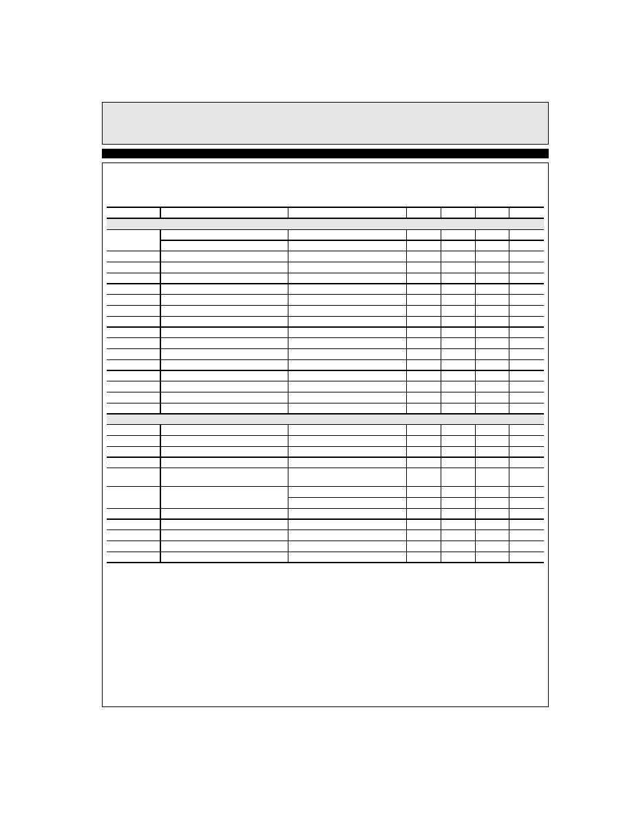
Electrical Characteristics
V
S
+ = +5V, V
S
- = -5V, T
A
= 25∞C, R
F
= 180
, R
G
= 20
, R
L
= 500
unless otherwise specified.
Parameter
Description
Conditions
Min
Typ
Max
Unit
DC Performance
V
OS
Input Offset Voltage (SO8)
0.2
2
mV
Input Offset Voltage (SOT23-5)
3
mV
T
CVOS
Offset Voltage Temperature Coefficient
17
µV/∞C
I
B
Input Bias Current
-10
-7
µA
I
OS
Input Bias Current Offset
0.06
0.6
µA
T
CIB
Input Bias Current Temperature Coefficient
0.013
µA/∞C
C
IN
Input Capacitance
2.2
pF
A
VOL
Open Loop Gain
V
O
= -2.5V to +2.5V
80
87
dB
PSRR
Power Supply Rejection Ratio
[1]
80
100
dB
CMRR
Common Mode Rejection Ratio
at CMIR
75
106
dB
CMIR
Common Mode Input Range
-4.6
3.8
V
V
OUTH
Positive Output Voltage Swing
No load, R
F
= 1k
3.8
3.8
V
V
OUTL
Negative Output Voltage Swing
No load, R
F
= 1k
-4
-3.9
V
V
OUTH2
Positive Output Voltage Swing
R
L
= 100
3.2
3.45
V
V
OUTL2
Negative Output Voltage Swing
R
L
= 100
-3.5
-3.2
V
I
OUT
Output Short Circuit Current
[2]
80
100
mA
I
SY
Supply Current
4.7
5.5
mA
AC Performance - R
G
= 20
, C
L
= 3pF
BW
-3dB Bandwidth, R
L
= 500
100
MHz
BW ±0.1dB
±0.1dB Bandwidth, R
L
= 500
17
MHz
BW ±1dB
±1dB Bandwidth, R
L
= 500
80
MHz
Peaking
Peaking, R
L
= 500
0.6
dB
SR
Slew Rate
V
OUT
= 2V
PP
, measured at 20% to 80%
80
110
V/µs
OS
Overshoot, 4Vpk-pk Output Square Wave
Positive
2.8
%
Negative
-7
%
t
S
Settling Time to 0.1% of ±1V Pulse
51
ns
V
N
Voltage Noise Spectral Density
1.3
nV/
Hz
I
N
Current Noise Spectral Density
1.2
pA/
Hz
HD2
2nd Harmonic Distortion
[3]
-70
dBc
HD3
3rd Harmonic Distortion
[3]
-70
dBc
1. Measured by moving the supplies from ±4V to ±6V
2. Pulse test only and using a 10
load
3. Frequency = 1MHz, V
OUT
= 2Vpk-pk, into 500
and 5pF load
3
EL2126C
Ultra-Low Noise, Low Power, Wideband Amplifier
E
L
2126C
Electrical Characteristics
V
S
+ = +15V, V
S
- = -15V, T
A
= 25∞C, R
F
= 180
, R
G
= 20
, R
L
= 500
unless otherwise specified.
Parameter
Description
Conditions
Min
Typ
Max
Unit
DC Performance
V
OS
Input Offset Voltage (SO8)
0.5
3
mV
Input Offset Voltage (SOT23-5)
3
mV
T
CVOS
Offset Voltage Temperature Coefficient
4.5
µV/∞C
I
B
Input Bias Current
-10
-7
µA
I
OS
Input Bias Current Offset
0.12
0.7
µA
T
CIB
Input Bias Current Temperature Coefficient
0.016
µA/∞C
C
IN
Input Capacitance
2.2
pF
A
VOL
Open Loop Gain
80
90
dB
PSRR
Power Supply Rejection Ratio
[1]
65
80
dB
CMRR
Common Mode Rejection Ratio
at CMIR
70
85
dB
CMIR
Common Mode Input Range
-14.6
13.8
V
V
OUTH
Positive Output Voltage Swing
No load, R
F
= 1k
13.6
13.7
V
V
OUTL
Negative Output Voltage Swing
No load, R
F
= 1k
-13.8
-13.7
V
V
OUTH2
Positive Output Voltage Swing
R
L
= 100
, R
F
= 1k
10.2
11.2
V
V
OUTL2
Negative Output Voltage Swing
R
L
= 100
, R
F
= 1k
-10.3
-9.5
V
I
OUT
Output Short Circuit Current
[2]
140
220
mA
I
SY
Supply Current
5
6
mA
AC Performance - R
G
= 20
, C
L
= 3pF
BW
-3dB Bandwidth, R
L
= 500
135
MHz
BW ±0.1dB
±0.1dB Bandwidth, R
L
= 500
26
MHz
BW ±1dB
±1dB Bandwidth, R
L
= 500
60
MHz
Peaking
Peaking, R
L
= 500
2.1
dB
SR
Slew Rate (±2.5V Square Wave, Measured
25%-75%)
130
150
V/µS
OS
Overshoot, 4Vpk-pk Output Square Wave
Positive
1.6
%
Negative
-4.4
%
T
S
Settling Time to 0.1% of ±1V Pulse
48
ns
V
N
Voltage Noise Spectral Density
1.4
nV/
Hz
I
N
Current Noise Spectral Density
1.1
pA/
Hz
HD2
2nd Harmonic Distortion
[3]
-72
dBc
HD3
3rd Harmonic Distortion
[3]
-73
dBc
1. Measured by moving the supplies from ±13.5V to ±16.5V
2. Pulse test only and using a 10
load
3. Frequency = 1MHz, V
OUT
= 2Vpk-pk, into 500
and 5pF load
4
EL2126C
Ultra-Low Noise, Low Power, Wideband Amplifier
E
L
21
26C
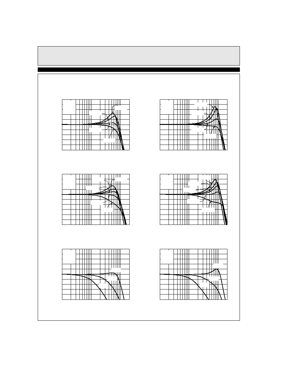
Typical Performance Curves
Non-Inverting Frequency Response for Various R
F
10
6
2
-2
-6
-10
1M
10M
100M
Frequency (Hz)
N
o
r
m
al
i
z
ed
G
a
i
n
(
d
B
)
R
F
=1k
R
F
=500
R
F
=180
R
F
=100
V
S
=±5V
A
V
=10
C
L
=5pF
R
L
=500
Non-Inverting Frequency Response for Various R
F
10
6
2
-2
-6
-10
1M
10M
100M
Frequency (Hz)
N
o
r
m
al
i
z
ed
G
a
i
n
(
d
B
)
R
F
=1k
R
F
=500
R
F
=180
R
F
=100
Inverting Frequency Response for Various R
F
8
4
0
-4
-8
-12
1M
10M
100M
Frequency (Hz)
N
o
r
m
al
i
z
ed
G
a
i
n
(
d
B
)
V
S
=±15V
A
V
=-10
C
L
=5pF
R
L
=500
Inverting Frequency Response for Various R
F
8
4
0
-4
-8
-12
1M
10M
100M
Frequency (Hz)
N
o
r
m
al
i
z
ed
G
a
i
n
(
d
B
)
V
S
=±5V
A
V
=-10
C
L
=5pF
R
L
=500
Non-Inverting Frequency Response for Various Gain
10
6
2
-2
-6
-10
1M
10M
100M
Frequency (Hz)
N
o
r
m
al
i
z
ed
G
a
i
n
(
d
B
)
A
V
=10
V
S
=±5V
R
G
=20
R
L
=500
C
L
=5pF
Non-Inverting Frequency Response for Various Gain
10
6
2
-2
-6
-10
1M
10M
100M
Frequency (Hz)
N
o
r
m
al
i
z
ed
G
a
i
n
(
d
B
)
R
F
=1k
R
F
=350
R
F
=100
R
F
=200
R
F
=500
R
F
=1k
R
F
=500
R
F
=200
R
F
=100
R
F
=350
A
V
=20
A
V
=50
V
S
=±15V
R
G
=20
R
L
=500
C
L
=5pF
A
V
=10
A
V
=20
A
V
=50
V
S
=±15V
A
V
=10
C
L
=5pF
R
L
=500
5
EL2126C
Ultra-Low Noise, Low Power, Wideband Amplifier
E
L
2126C
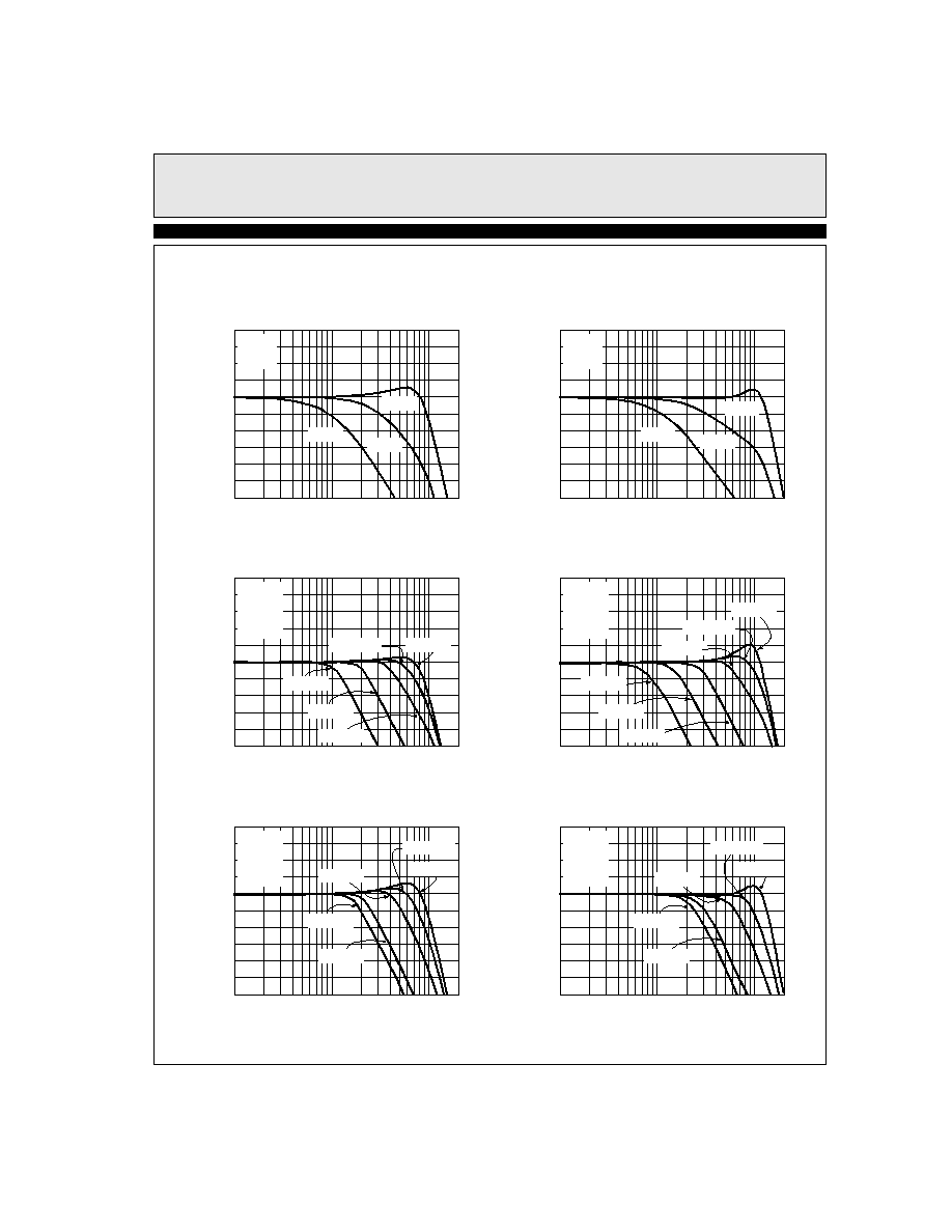
Typical Performance Curves
Inverting Frequency Response for Various Gain
8
4
0
-4
-8
-12
1M
10M
100M
Frequency (Hz)
N
o
r
m
al
i
z
ed
G
a
i
n
(
d
B
)
Inverting Frequency Response for Various R
F
8
4
0
-4
-8
-12
1M
10M
100M
Frequency (Hz)
N
o
r
m
al
i
z
ed
G
a
i
n
(
d
B
)
Non-Inverting Frequency Response for Various Output
Signal Levels
10
6
2
-2
-6
-10
1M
10M
100M
Frequency (Hz)
N
o
r
m
al
i
z
ed
G
a
i
n
(
d
B
)
Non-Inverting Frequency Response for Various Output
Signal Levels
8
4
0
-4
-8
-12
1M
10M
100M
Frequency (Hz)
N
o
r
m
al
i
z
ed
G
a
i
n
(
d
B
)
Inverting Frequency Response for Various Output Signal
Levels
8
4
0
-4
-8
-12
1M
10M
100M
Frequency (Hz)
N
o
r
m
al
i
z
ed
G
a
i
n
(
d
B
)
Inverting Frequency Response for Various Output Signal
Levels
8
4
0
-4
-8
-12
1M
10M
100M
Frequency (Hz)
N
o
r
m
al
i
z
ed
G
a
i
n
(
d
B
)
V
S
=±5V
C
L
=5pF
R
G
=35
A
V
=-10
A
V
=-20
A
V
=-50
V
S
=±15V
C
L
=5pF
R
G
=20
A
V
=-10
A
V
=-20
A
V
=-50
V
S
=±5V
C
L
=5pF
R
L
=500
R
F
=180
A
V
=10
V
O
=2.5V
PP
V
O
=5V
PP
V
O
=1V
PP
V
O
=30mV
PP
V
O
=500mV
PP
V
S
=±15V
C
L
=5pF
R
L
=500
R
F
=180
A
V
=10
V
O
=5V
PP
V
O
=1V
PP
V
O
=2.5V
PP
V
O
=30mV
PP
V
O
=500mV
PP
V
O
=10V
PP
V
S
=±5V
C
L
=5pF
R
L
=500
R
F
=350
A
V
=10
V
O
=3.4V
PP
V
O
=1V
PP
V
O
=2.5V
PP
V
O
=30mV
PP
V
O
=500mV
PP
V
S
=±15V
C
L
=5pF
R
L
=500
R
F
=200
A
V
=10
V
O
=3.4V
PP
V
O
=1V
PP
V
O
=2.5V
PP
V
O
=30mV
PP
V
O
=500mV
PP