 | –≠–ª–µ–∫—Ç—Ä–æ–Ω–Ω—ã–π –∫–æ–º–ø–æ–Ω–µ–Ω—Ç: EL2157C | –°–∫–∞—á–∞—Ç—å:  PDF PDF  ZIP ZIP |
EL2150CEL2157C
June
1996
Rev
B
EL2150C EL2157C
125 MHz Single Supply Clamping Op Amps
Note All information contained in this data sheet has been carefully checked and is believed to be accurate as of the date of publication however this data sheet cannot be a ``controlled document'' Current revisions if any to these
specifications are maintained at the factory and are available upon your request We recommend checking the revision level before finalization of your design documentation
1995 Elantec Inc
Features
Specified for
a
3V
a
5V or
g
5V Applications
Power Down to 0 mA (EL2157C)
Output Voltage Clamp
(EL2157C)
Large Input Comon Mode Range
0V
k
V
CM
k
Vs - 1 2V
Output Swings to Ground
Without Saturating
b
3 dB Bandwidth
e
125 MHz
g
0 1 dB Bandwidth
e
30 MHz
Low Supply Current
e
5 mA
Slew Rate
e
275V
ms
Low Offset Voltage
e
2 mV max
(PDIP and SO Packages)
Output Current
e
g
100 mA
High Open Loop Gain
e
80 dB
Differential Gain
e
0 05%
Differential Phase
e
0 05
Applications
Video Amplifier
PCMCIA Applications
A D Driver
Line Driver
Portable Computers
High Speed Communications
RGB Applications
Broadcast Equipment
Active Filtering
Ordering Information
Part No
Temp Range
Package
Outline
EL2150CN
b
40 C to
a
85 C 8 Pin PDIP
MDP0031
EL2150CS
b
40 C to
a
85 C 8 Pin SOIC
MDP0027
EL2150CW
b
40 C to
a
85 C 5 Pin SOT23
MDP0038
EL2157CN
b
40 C to
a
85 C 8 Pin PDIP
MDP0031
EL2157CS
b
40 C to
a
85 C 8 Pin SOIC
MDP0027
See
Ordering
Information
section
of
databook
General Description
The EL2150C EL2157C are the electronics industry's fastest
single supply op amps available Prior single supply op amps
have generally been limited to bandwidths and slew rates
that of the EL2150C EL2157C
The 125 MHz bandwidth
275 V
ms slew rate and 0 05% 0 05 differential gain differen-
tial phase makes this part ideal for single or dual supply video
speed applications With its voltage feedback architecture this
amplifier can accept reactive feedback networks allowing them
to be used in analog filtering applications The inputs can sense
signals below the bottom supply rail and as high as 1 2V below
the top rail Connecting the load resistor to ground and operat-
ing from a single supply the outputs swing completely to
ground without saturating The outputs can also drive to within
1 2V of the top rail The EL2150C EL2157C will output
g
100
mA and will operate with single supply voltages as low as 2 7V
making it ideal for portable low power applications
The EL2157C has a high speed disable feature Applying a low
logic level to this pin reduces the supply current to 0
mA within
50 ns This is useful for both multiplexing and reducing power
consumption
The EL2157C also has an output voltage clamp feature This
clamp is a fast recovery (
k
7 ns) output clamp that prevents the
output voltage from going above the preset clamp voltage This
feature is desirable for A D applications as A D converters can
require long times to recover if overdriven
For applications where board space is critical the EL2150C is
available in the tiny 5 lead SOT23 package which has a foot-
print 28% the size of an 8 lead SOIC The EL2150C EL2157C
are also both available in 8 pin plastic DIP and SOIC packages
All parts operate over the industrial temperature range of
b
40 C to
a
85 C For dual triple or quad applications contact
the factory
Connection Diagrams
EL2150C
EL2157C
EL2150C
SO P-DIP
SO P-DIP
SOT23-5
2150 ≠ 3
2150 ≠ 2
2150 ≠ 1
Top View
Top View
Top View
EL2150C EL2157C
125 MHz Single Supply Clamping Op Amps
Absolute Maximum Ratings
(T
A
e
25 C)
Supply Voltage between V
Sa
and GND
a
12 6V
Input Voltage (IN
a
IN
b
ENABLE CLAMP)
GND
b
0 3V V
S
a
0 3V
Differential Input Voltage
g
6V
Maximum Output Current
90 mA
Output Short Circuit Duration
(note 1)
Power Dissipation
See Curves
Storage Temperature Range
b
65 C to
a
150 C
Ambient Operating Temperature Range
b
40 C to
a
85 C
Operating Junction Temperature
150 C
Important Note
All parameters having Min Max specifications are guaranteed The Test Level column indicates the specific device testing actually
performed during production and Quality inspection Elantec performs most electrical tests using modern high-speed automatic test
equipment specifically the LTX77 Series system Unless otherwise noted all tests are pulsed tests therefore T
J
e
T
C
e
T
A
Test Level
Test Procedure
I
100% production tested and QA sample tested per QA test plan QCX0002
II
100% production tested at T
A
e
25 C and QA sample tested at T
A
e
25 C
T
MAX
and T
MIN
per QA test plan QCX0002
III
QA sample tested per QA test plan QCX0002
IV
Parameter is guaranteed (but not tested) by Design and Characterization Data
V
Parameter is typical value at T
A
e
25 C for information purposes only
DC Electrical Characteristics
(Note 2) V
S
e a
5V GND
e
0V T
A
e
25 C V
CM
e
1 5V V
OUT
e
1 5V V
CLAMP
e a
5V V
ENABLE
e a
5V unless otherwise specified
Parameter
Description
Conditions
Min Typ Max
Test
Units
Level
V
OS
Offset Voltage
PDIP and SOIC Packages
b
2
2
I
mV
SOT23-5 Package
b
3
3
I
mV
TCV
OS
Offset Voltage Temperature Coefficient
Measured from Tmin to Tmax
10
V
mV C
IB
Input Bias Current
V
IN
e
0V
b
5 5
b
10
I
mA
I
OS
Input Offset Current
V
IN
e
0V
b
750 150
750
I
nA
TCI
OS
Input Bias Current Temperature Coefficient Measured from Tmin to Tmax
50
V
nA C
PSRR
Power Supply Rejection Ratio
V
S
e
V
ENABLE
e a
2 7V to
a
12V
55
70
I
dB
V
CLAMP
e
OPEN
CMRR
Common Mode Rejection Ratio
VCM
e
0V to
a
3 8V
55
65
I
dB
VCM
e
0V to
a
3 0V
55
70
I
dB
CMIR
Common Mode Input Range
0
V
S
b
1 2
I
V
R
IN
Input Resistance
Common Mode
1
2
I
M
X
C
IN
Input Capacitance
SOIC Package
1
V
pF
PDIP Package
1 5
V
pF
R
OUT
Output Resistance
Av
e a
1
40
V
m
X
I
S ON
Supply Current
Enabled
V
S
e
V
CLAMP
e a
12V V
ENABLE
e a
12V
5
6 5
I
mA
I
S OFF
Supply Current
Shut Down
V
S
e
V
CLAMP
e a
10V V
ENABLE
e a
0 5V
0
50
I
mA
V
S
e
V
CLAMP
e a
12V V
ENABLE
e a
0 5V
5
V
mA
PSOR
Power Supply Operating Range
2 7
12 0
I
v
2
TAB
WIDE
TD
is
38in
EL2150C EL2157C
125 MHz Single Supply Clamping Op Amps
DC Electrical Characteristics
Contd
(Note 2) V
S
e a
5V GND
e
0V T
A
e
25 C V
CM
e a
1 5V V
OUT
e a
1 5V V
CLAMP
e a
5V V
ENABLE
e a
5V unless otherwise
specified
Parameter
Description
Conditions
Min Typ Max
Test
Units
Level
PSOR
Power Supply Operating Range
2 7
12 0
I
V
AVOL
Open Loop Gain
V
S
e
V
CLAMP
e a
12V V
OUT
e a
2V to
65
80
I
dB
a
9V R
L
e
1 k
X to GND
V
OUT
e a
1 5V to
a
3 5V
70
V
dB
R
L
e
1 k
X to GND
V
OUT
e a
1 5V to
a
3 5V
60
V
dB
R
L
e
150
X to GND
V
OP
Positive Output Voltage Swing
V
S
e a
12V A
V
e a
1 R
L
e
1 k
X to 0V
10 8
V
V
V
S
e a
12V A
V
e a
1 R
L
e
150
X to 0V
9 6
10 0
I
V
V
S
e
g
5V A
V
e a
1 R
L
e
1 k
X to 0V
4 0
V
V
V
S
e
g
5V A
V
e a
1 R
L
e
150
X to 0V
3 4
3 8
I
V
V
S
e a
3V A
V
e a
1 R
L
e
150
X to 0V
1 8
1 95
I
V
V
ON
Negative Output Voltage Swing
V
S
e a
12V A
V
e a
1 R
L
e
150
X to 0V
5 5
8
I
mV
V
S
e
g
5V A
V
e a
1 R
L
e
1 k
X to 0V
b
4 0
V
V
V
S
e
g
5V A
V
e a
1 R
L
e
150
X to 0V
b
3 7
b
3 4
I
V
I
OUT
Output Current (Note 1)
V
S
e
g
5V A
V
e a
1 R
L
e
10
X to 0V
g
75
g
100
I
mA
V
S
e
g
5V A
V
e a
1 R
L
e
50
X to 0V
g
60
V
mA
I
OUT OFF
Output Current Disabled
V
ENABLE
e a
0 5V
0
20
I
mA
V
IH-EN
ENABLE pin Voltage for Power Up
Relative to GND pin
2 0
I
V
V
IL-EN
ENABLE pin Voltage for Shut Down
Relative to GND pin
0 5
I
V
I
IH-EN
ENABLE pin Input Current-High (Note 3) V
S
e
V
CLAMP
e a
12V V
ENABLE
e a
12V
340
410
I
mA
I
IL-EN
ENABLE pin Input Current-Low (Note 3) V
S
e
V
CLAMP
e a
12V V
ENABLE
e a
0 5V
0
1
I
mA
V
OR-CL
Voltage Clamp Operating Range (Note 4)
Relative to GND pin
1 2
V
OP
I
V
V
ACC-CL
CLAMP Accuracy (Note 5)
V
IN
e a
4V R
L
e
1 k
X to GND
b
250 100
250
I
mV
V
CLAMP
e a
1 5V and
a
3 5V
I
IH-CL
CLAMP pin Input Current
High
V
S
e
V
CLAMP
e a
12V
12
25
I
mA
I
IL-CL
CLAMP pin Input Current
Low
V
S
e a
12V V
CLAMP
e a
1 2V
b
20
b
15
I
mA
3
TD
is
52in

EL2150C EL2157C
125 MHz Single Supply Clamping Op Amps
Closed Loop AC Electrical Characteristics
(Notes 2
6) V
S
e a
5V GND
e
0V T
A
e
25 C V
CM
e a
1 5V V
OUT
e a
1 5V V
CLAMP
e a
5V V
ENABLE
e a
5V A
V
e a
1
R
F
e
0
X R
L
e
150
X to GND pin unless otherwise specified
Parameter
Description
Conditions
Min Typ Max
Test
Units
Level
BW
b
3 dB Bandwidth (V
OUT
e
400 mVp-p)
V
S
e a
5V A
V
e a
1 R
F e
0
X
125
V
MHz
V
S
e a
5V A
V
e b
1 R
F
e
500
X
60
V
MHz
V
S
e a
5V A
V
e a
2 R
F
e
500
X
60
V
MHz
V
S
e a
5V A
V
e a
10 R
F
e
500
X
6
V
MHz
V
S
e a
12V A
V
e a
1 R
F
e
0
X
150
V
MHz
V
S
e a
3V A
V
e a
1 R
F
e
0
X
100
V
MHz
BW
g
0 1 dB Bandwidth (V
OUT
e
400 mVp-p) V
S
e a
12V A
V
e a
1 R
F
e
0
X
25
V
MHz
V
S
e a
5V A
V
e a
1 R
F
e
0
X
30
V
MHz
V
S
e a
3V A
V
e a
1 R
F
e
0
X
20
V
MHz
GBWP
Gain Bandwidth Product
V
S
e a
12V
A
V
e a
10
60
V
MHz
PM
Phase Margin
R
L
e
1 k
X CL
e
6 pF
55
V
SR
Slew Rate
V
S
e a
10V R
L
e
150
X V
out
e
0V to
a
6V
200 275
I
V
ms
V
S
e a
5V R
L
e
150
X V
OUT
e
0V to
a
3V
300
V
V
ms
t
R
t
F
Rise Time Fall Time
g
0 1V step
2 8
V
ns
OS
Overshoot
g
0 1V step
10
V
%
t
PD
Propagation Delay
g
0 1V step
3 2
V
ns
t
S
0 1% Settling Time
V
S
e
g
5V R
L
e
500
X A
V
e a
1 V
OUT
e
g
3V
40
V
ns
0 01% Settling Time
V
S
e
g
5V R
L
e
500
X A
V
e a
1 V
OUT
e
g
3V
75
V
ns
dG
Differential Gain (Note 7)
A
V
e a
2 R
F
e
1 k
X
0 05
V
%
dP
Differential Phase (Note 7)
A
V
e a
2 R
F
e
1 k
X
0 05
V
e
N
Input Noise Voltage
f
e
10 kHz
48
V
nV
0
Hz
i
N
Input Noise Current
f
e
10 kHz
1 25
V
pA
0
Hz
t
DIS
Disable Time (Note 8)
50
V
ns
t
EN
Enable Time (Note 8)
25
V
ns
t
CL
Clamp Overload Recovery
7
V
ns
Note 1 Internal short circuit protection circuitry has been built into the EL2150C EL2157C See the Applications section
Note 2 CLAMP pin and ENABLE pin specifications apply only to the EL2157C
Note 3 If the disable feature is not desired tie the ENABLE pin to the V
S
pin or apply a logic high level to the ENABLE pin
Note 4 The maximum output voltage that can be clamped is limited to the maximum positive output Voltage or V
OP
Applying a
Voltage higher than V
OP
inactivates the clamp If the clamp feature is not desired either tie the CLAMP pin to the V
S
pin
or simply let the CLAMP pin float
Note 5 The clamp accuracy is affected by V
IN
and R
L
See the Typical Curves Section and the Clamp Accuracy vs V
IN
R
L
curve
Note 6 All AC tests are performed on a ``warmed up'' part except slew rate which is pulse tested
Note 7 Standard NTSC signal
e
286 mVp-p f
e
3 58MHz as VIN is swept from 0 6V to 1 314V R
L
is DC coupled
Note 8 Disable Enable time is defined as the time from when the logic signal is applied to the ENABLE pin to when the supply
current has reached half its final value
4
TD
is
51in

EL2150C EL2157C
125 MHz Single Supply Clamping Op Amps
Typical Performance Curves
Non-Inverting
Frequency Response (Gain)
Frequency Response (Phase)
Non-Inverting
Non-Inverting Gains
Temperature for
3 dB Bandwidth vs
Response (Gain)
Inverting Frequency
Response (Phase)
Inverting Frequency
Inverting Gains
Temperature for
3 dB Bandwidth vs
for Various R
L
Frequency Response
for Various C
L
Frequency Response
Common Mode Voltage
Frequency Response vs
Non-Inverting
2150 ≠ 74
5

EL2150C EL2157C
125 MHz Single Supply Clamping Op Amps
Typical Performance Curves
Contd
Supply Voltage for
3 dB Bandwidth vs
Non-Inverting Gains
A
V
e
a
1
Various Supply Voltages
Frequency Response for
vs Frequency
PSSR and CMRR
Voltage for Inverting Gains
3 dB Bandwith vs Supply
A
V
e
a
2
Various Supply Voltages
Frequency Response for
Die Temperature
PSRR and CMRR vs
Phase vs Frequency
Open Loop Gain and
vs Die Temperature
Open Loop Voltage Gain
Impedance vs Frequency
Closed Loop Output
2150 ≠ 75
6

EL2150C EL2157C
125 MHz Single Supply Clamping Op Amps
Typical Performance Curves
Contd
V
S
e
a
3V
Large Signal Step Response
V
S
e
a
5V
Large Signal Step Response
V
S
e
a
12V
Large Signal Step Response
Small Signal Step Response
V
S
e
g
5V
Large Signal Step Response
Slew Rate vs Temperature
Settling Accuracy
Settling Time vs
vs Frequency
Voltage and Current Noise
2150 ≠ 76
7
EL2150C EL2157C
125 MHz Single Supply Clamping Op Amps
Typical Performance Curves
Contd
Differential Gain for
Single Supply Operation
Single Supply Operation
Differential Phase for
for Dual Supply Operation
Differential Gain and Phase
Distortion vs Frequency
2nd and 3rd Harmonic
Distortion vs Frequency
2nd and 3rd Harmonic
Distortion vs Frequency
2nd and 3rd Harmonic
Frequency for THD
k
0 1%
Output Voltage Swing vs
Distortion
Frequency for Unlimited
Output Voltage Swing vs
vs Die Temperature
Output Current
2150 ≠ 77
8

EL2150C EL2157C
125 MHz Single Supply Clamping Op Amps
Typical Performance Curves
Contd
Supply Current vs
Supply Voltage
Die Temperature
Supply Current vs
Die Temperature
Input Resistance vs
Die Temperature (4 Samples)
Offset Voltage vs
vs Input Voltage
Input Bias Current
vs Die Temperature
and Input Bias Current
Input Offset Current
R
L
e
150X to GND
Swing vs Die Temperature
Positive Output Voltage
R
L
e
150X to GND
Swing vs Die Temperature
Negative Output Voltage
vs Die Temperature
Clamp Accuracy
2150 ≠ 78
9

EL2150C EL2157C
125 MHz Single Supply Clamping Op Amps
Typical Performance Curves
Contd
R
L
e
150X
Clamp Accuracy
2150 ≠ 48
R
L
e
1 kX
Clamp Accuracy
2150 ≠ 49
R
L
e
10 kX
Clamp Accuracy
2150 ≠ 50
Family of DC Inputs
Enable Response for a
2150 ≠ 51
Family of DC Inputs
Disable Response for a
2150 ≠ 52
Disable Enable Response for a
Family of Sine Waves
2150 ≠ 53
OFF Isolation
2150 ≠ 72
10
EL2150C EL2157C
125 MHz Single Supply Clamping Op Amps
Typical Performance Curves
Contd
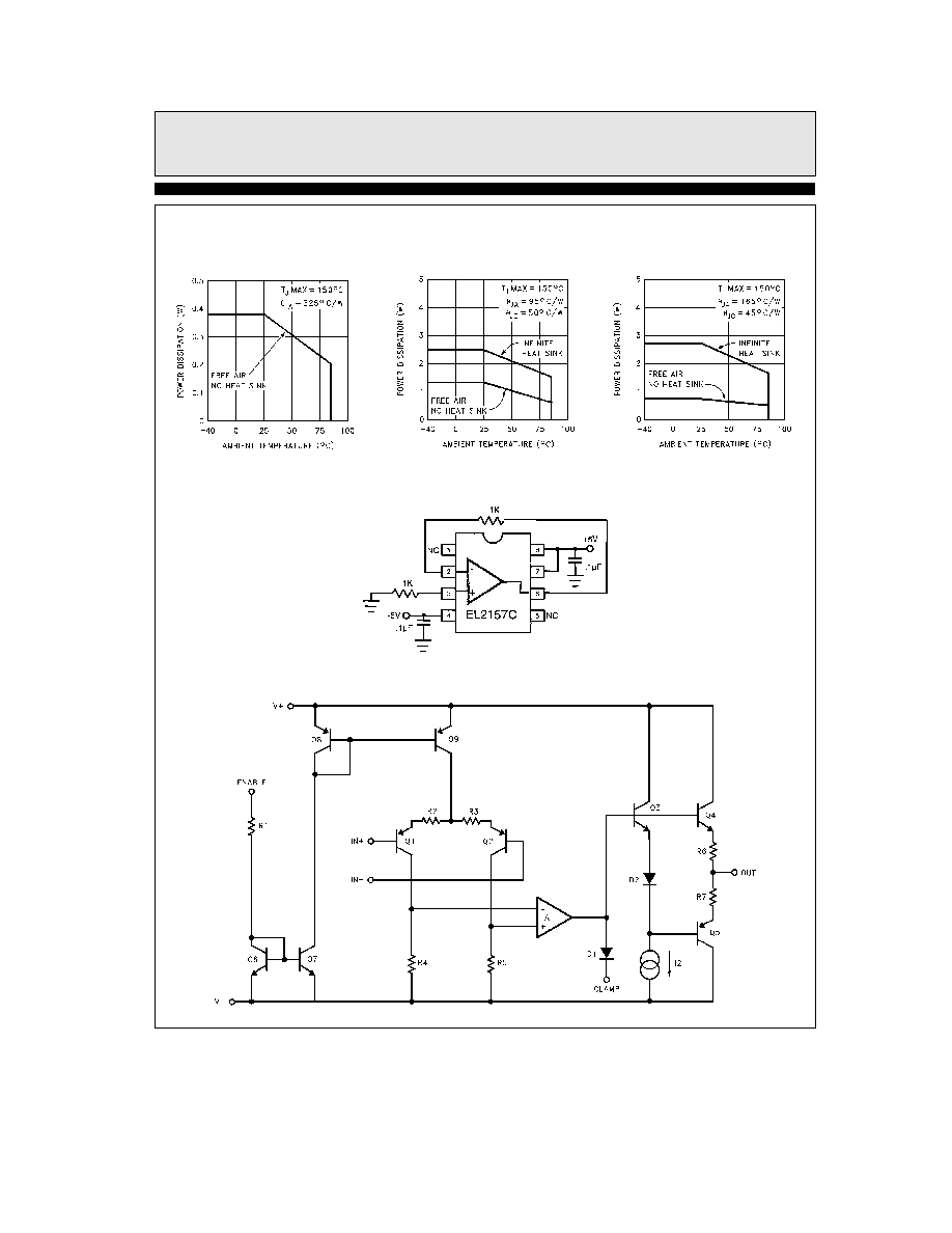
vs Ambient Temperature
Maximum Power Dissipation
5-Lead Plastic SOT23
2150 ≠ 54
vs Ambient Temperature
Maximum Power Dissipation
8-Lead Plastic DIP
2150 ≠ 55
vs Ambient Temperature
Maximum Power Dissipation
8-Lead Plastic SO
2150 ≠ 56
Burn-In Circuit
2150 ≠ 57
Simplified Schematic
2150 ≠ 58
11

EL2150C EL2157C
125 MHz Single Supply Clamping Op Amps
Applications Information
Product Description
The EL2150C EL2157C are the industry's fastest
single supply operational amplifiers Connected
in voltage follower mode their
b
3dB bandwidth
is 125 MHz while maintaining a 275 V
ms slew
rate With an input and output common mode
range that includes ground these amplifiers were
optimized for single supply operation but will
also accept dual supplies They operate on a total
supply voltage range as low as
a
2 7V or up to
a
12V This makes them ideal for
a
3V applica-
tions especially portable computers
While many amplifiers claim to operate on a sin-
gle supply and some can sense ground at their
inputs most fail to truly drive their outputs to
ground If they do succeed in driving to ground
the amplifier often saturates causing distortion
and recovery delays However special circuitry
built into the EL2150C EL2157C allows the out-
put to follow the input signal to ground without
recovery delays
Power Supply Bypassing And Printed
Circuit Board Layout
As with any high-frequency device good printed
circuit board layout is necessary for optimum
performance Ground plane construction is high-
ly recommended Lead lengths should be as short
as possible The power supply pins must be well
bypassed to reduce the risk of oscillation The
combination of a 4 7
mF tantalum capacitor in
parallel with a 0 1
mF ceramic capacitor has been
shown to work well when placed at each supply
pin For single supply operation where pin 4
(V
S
b
) is connected to the ground plane a single
4 7
mF tantalum capacitor in parallel with a 0 1
mF ceramic capacitor across pins 7 and 4 will suf-
fice
For good AC performance parasitic capacitance
should be kept to a minimum Ground plane con-
struction should be used Carbon or Metal-Film
resistors are acceptable with the Metal-Film re-
sistors giving slightly less peaking and band-
width because of their additional series induc-
tance Use of sockets particularly for the SO
package should be avoided if possible Sockets
add parasitic inductance and capacitance which
will result in some additional peaking and over-
shoot
Supply Voltage Range and
Single-Supply Operation
The EL2150C EL2157C have been designed to
operate with supply voltages having a span of
greater than 2 7V and less than 12V In practical
terms this means that the EL2150C EL2157C
will operate on dual supplies ranging from
g
1 35V to
g
6V
With a single-supply
the
EL2150C EL2157C will operate from
a
2 7V to
a
12V Performance has been optimized for a sin-
gle
a
5V supply
Pins 7 and 4 are the power supply pins The posi-
tive power supply is connected to pin 7 When
used in single supply mode pin 4 is connected to
ground When used in dual supply mode the neg-
ative power supply is connected to pin 4
As supply voltages continue to decrease it be-
comes necessary to provide input and output
voltage ranges that can get as close as possible to
the supply voltages
The EL2150C EL2157C
have an input voltage range that includes the
negative supply and extends to within 1 2V of the
positive supply So for example on a single
a
5V
supply the EL2150C EL2157C have an input
range which spans from 0V to 3 8V
The output range of the EL2150C EL2157C is
also quite large It includes the negative rail and
extends to within 1V of the top supply rail On a
a
5V supply the output is therefore capable of
swinging from 0V to
a
4V On split supplies the
output will swing
g
4V If the load resistor is tied
to the negative rail and split supplies are used
the output range is extended to the negative rail
Choice Of Feedback Resistor R
F
The feedback resistor forms a pole with the input
capacitance As this pole becomes larger phase
margin is reduced This increases ringing in the
time domain and peaking in the frequency do-
main Therefore R
F
has some maximum value
which should not be exceeded for optimum per-
formance If a large value of R
F
must be used a
small capacitor in the few picofarad range in par-
allel with R
F
can help to reduce this ringing and
peaking at the expense of reducing the band-
width
12

EL2150C EL2157C
125 MHz Single Supply Clamping Op Amps
Applications Information
Contd
As far as the output stage of the amplifier is con-
cerned R
F
a
R
G
appear in parallel with R
L
for
gains other than
a
1 As this combination gets
smaller the bandwidth falls off Consequently
R
F
has a minimum value that should not be ex-
ceeded for optimum performance
For A
V
e a
1 R
F
e
0
X is optimum For Av
e
b
1 or
a
2 (noise gain of 2) optimum response is
obtained with R
F
between 500
X and 1 kX For
Av
e
b
4 or
a
5 (noise gain of 5) keep R
F
be-
tween 2 k
X and 10 kX
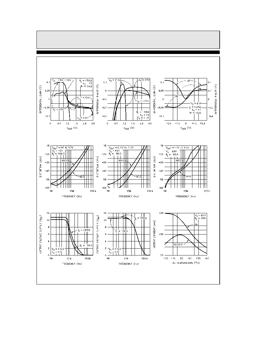
Video Performance
For good video performance an amplifier is re-
quired to maintain the same output impedance
and the same frequency response as DC levels are
changed at the output This can be difficult when
driving a standard video load of 150
X because of
the change in output current with DC level Dif-
ferential Gain and Differential Phase for the
EL2150C EL2157C are specified with the black
level of the output video signal set to
a
1 2V
This allows ample room for the sync pulse even
in a gain of
a
2 configuration This results in dG
and dP specifications of 0 05% and 0 05 while
driving 150
X at a gain of
a
2 Setting the black
level to other values although acceptable will
compromise peak performance
For example
looking at the single supply dG and dP curves for
R
L
e
150
X if the output black level clamp is re-
duced from 1 2V to 0 6V dG dP will increase
from 0 05% 0 05 to 0 08% 0 25 Note that in a
gain of
a
2 configuration this is the lowest black
level allowed such that the sync tip doesn't go
below 0V
If your application requires that the output goes
to
ground
then
the
output
stage
of
the
EL2150C EL2157C like all other single supply
op amps requires an external pull down resistor
tied to ground As mentioned above the current
flowing through this resistor becomes the DC
bias current for the output stage NPN transistor
As this current approaches zero the NPN turns
off and dG and dP will increase This becomes
more critical as the load resistor is increased in
value While driving a light load such as 1 k
X if
the input black level is kept above 1 25V dG and
dP are a respectable 0 03% and 0 03
For other biasing conditions see the Differential
Gain and Differential Phase vs Input Voltage
curves
Output Drive Capability
In spite of their moderately low 5 mA of supply
current the EL2150C EL2157C are capable of
providing
g
100 mA of output current into a 10
X
load or
g
60 mA into 50
X With this large output
current capability a 50
X load can be driven to
g
3V with V
S
e
g
5V making it an excellent
choice for driving isolation transformers in tele-
communications applications
Driving Cables and Capacitive Loads
When used as a cable driver double termination
is always recommended for reflection-free per-
formance For those applications the back-termi-
nation
series
resistor
will
de-couple
the
EL2150C EL2157C from the cable and allow ex-
tensive capacitive drive However other applica-
tions may have high capacitive loads without a
back-termination resistor In these applications a
small series resistor (usually between 5
X and
50
X) can be placed in series with the output to
eliminate most peaking The gain resistor (R
G
)
can then be chosen to make up for any gain loss
which may be created by this additional resistor
at the output
Disable Power-Down
The EL2157C amplifier can be disabled placing
its output in a high-impedance state The disable
or enable action takes only about 40 nsec When
disabled
the amplifier's supply current is re-
duced to 0 mA thereby eliminating all power
consumption by the EL2157C The EL2157C am-
plifier's power down can be controlled by stan-
dard CMOS signal levels at the ENABLE pin
The applied CMOS signal is relative to the GND
pin For example if a single
a
5V supply is used
the logic voltage levels will be
a
0 5V and
a
2 0V
If using dual
g
5V supplies the logic levels will
be
b
4 5V and
b
3 0V Letting the ENABLE pin
float will disable the EL2157C If the power-
down feature is not desired connect the EN-
ABLE pin to the V
S
a
pin The guaranteed logic
levels of
a
0 5V and
a
2 0V are not standard TTL
levels of
a
0 8V and
a
2 0V so care must be tak-
en if standard TTL will be used to drive the EN-
ABLE pin
13
EL2150C EL2157C
125 MHz Single Supply Clamping Op Amps
Applications Information
Contd
Output Voltage Clamp
The EL2157C amplifier has an output voltage
clamp This clamping action is fast being acti-
vated almost instantaneously and being deacti-
vated in
k
7 ns and prevents the output voltage
from going above the preset clamp voltage This
can be very helpful when the EL2157C is used to
drive an A D converter as some converters can
require long times to recover if overdriven The
output voltage remains at the clamp voltage level
as long as the product of the input voltage and
the gain setting exceeds the clamp voltage If the
EL2157C is connected in a gain of 2 for example
and
a
3V DC is applied to the CLAMP pin any
voltage higher than
a
1 5V at the inputs will be
clamped and
a
3V will be seen at the output
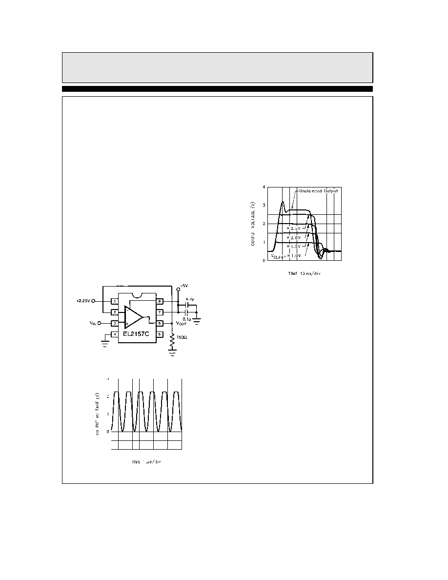
Figure 1 below is a unity gain connected
EL2157C being driven by a 3Vp-p sinewave with
2 25V applied to the CLAMP pin The resulting
output waveform with its output being clamped
to 2 25V is shown in Figure 2
2150 ≠ 59
Figure 1
2150 ≠ 60
Figure 2
Figure 3 shows the output of the same circuit
being driven by a 0 5V to 2 75V square wave as
the clamp voltage is varied from 1 0V to 2 5V as
well as the unclamped output signal The rising
edge of the signal is clamped to the voltage ap-
plied to the CLAMP pin almost instantaneously
The output recovers from the clamped mode
within 5 - 7 ns depending on the clamp voltage
Even when the CLAMP pin is taken 0 2V below
the minimum 1 2V specified the output is still
clamped and recovers in about 11 ns
2150 ≠ 61
Figure 3
The clamp accuracy is affected by 1) the CLAMP
pin voltage 2) the input voltage and 3) the load
resistor Depending upon the application the ac-
curacy may be as little as a few tens of millivolts
to a few hundred millivolts Be sure to allow for
these inaccuracies when choosing the clamp volt-
age Curves of Clamp Accuracy vs V
CLAMP
and
V
IN
for 3 values of R
L
are included in the Typi-
cal Performance Curves Section
Unlike amplifiers that clamp at the input and are
therefore limited to non-inverting applications
only
the EL2157C output clamp architecture
works for both inverting and non-inverting gain
applications There is also no maximum voltage
difference limitation between V
IN
and V
CLAMP
which is common on input clamped architec-
tures
The voltage clamp operates for any voltage be-
tween
a
1 2V above the GND pin and the mini-
mum output voltage swing V
OP
Forcing the
CLAMP pin much below
a
1 2V can saturate
transistors and should therefore be avoided
14
EL2150C EL2157C
125 MHz Single Supply Clamping Op Amps
Applications Information
Contd
Forcing the CLAMP pin above V
OP
simply de-
activates the CLAMP feature In other words
one cannot expect to clamp any voltage higher
than what the EL2157C can drive to in the first
place If the clamp feature is not desired either
let the CLAMP pin float or connect it to the V
S
a
pin
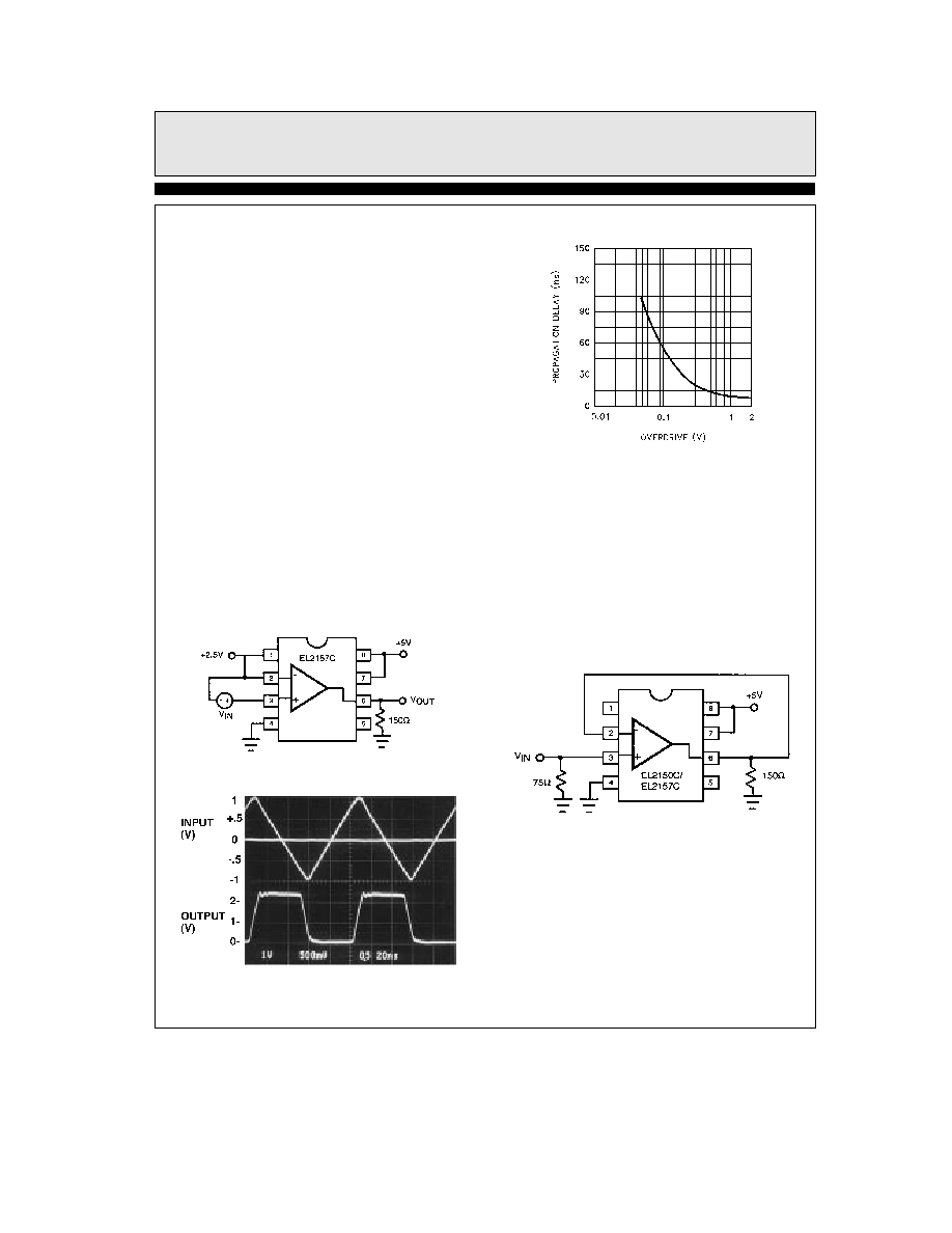
EL2157C Comparator Application
The EL2157C can be used as a very fast single
supply comparator by utilizing the clamp fea-
ture Most op amps used as comparators allow
only slow speed operation because of output satu-
ration issues However by applying a DC voltage
to the CLAMP pin of the EL2157C the maxi-
mum output voltage can be clamped thus pre-
venting
saturation
Figure
4
below
is
the
EL2157C implemented as a comparator 2 5V DC
is applied to the CLAMP pin as well as the IN
b
pin A differential signal is then applied between
the inputs Figure 5 shows the output square
wave that results when a
g
1V 10 MHz triangu-
lar wave is applied while Figure 6 is a graph of
propagation delay vs overdrive as a square wave
is presented at the input
2150 ≠ 62
Figure 4
2150 ≠ 63
Figure 5
EL2157 as a Comparator
Propagation Delay vs Overdrive
2150 ≠ 64
Figure 6
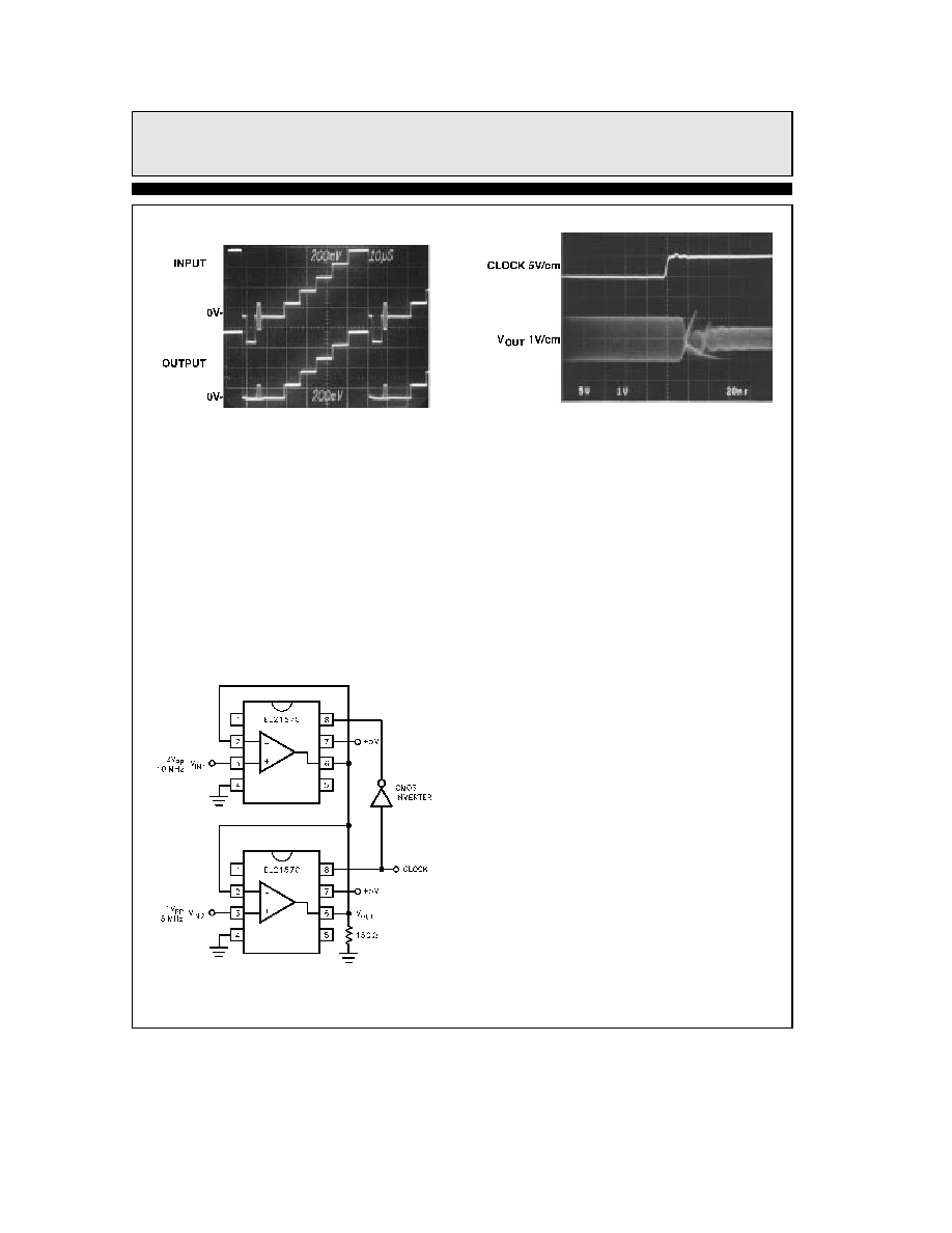
Video Sync Pulse Remover Application
All CMOS Analog to Digital Converters (A Ds)
have a parasitic latch-up problem when subjected
to negative input voltage levels Since the sync
tip contains no useful video information and it is
a negative going pulse we can chop it off Figure
7 shows a unity gain connected EL2150C
EL2157C Figure 8 shows the complete input vid-
eo signal applied at the input as well as the out-
put signal with the negative going sync pulse re-
moved
2150 ≠ 65
Figure 7
15
EL2150C EL2157C
125 MHz Single Supply Clamping Op Amps
Applications Information
Contd
2150 ≠ 66
Figure 8
Multiplexing with the EL2157C
The ENABLE pin on the EL2157C allows for
multiplexing applications Figure 9 shows two
EL2157Cs with their outputs tied together driv-
ing a back terminated 75
X video load A 2 Vp-p
10 MHz sinewave is applied at one input and a
1 Vp-p 5 MHz sinewave to the other Figure 10
shows the CLOCK signal which is applied and
the resulting output waveform at V
OUT
Switch-
ing is complete in about 50 ns Notice the outputs
are tied directly together Decoupling resistors at
each output are not necessary In fact adding
them approximately doubles the switching time
to 100 nsec
2150 ≠ 67
Figure 9
2150 ≠ 68
Figure 10
Short Circuit Current Limit
The EL2150C EL2157C have internal short cir-
cuit protection circuitry that protect it in the
event of its output being shorted to either supply
rail This limit is set to around 100 mA nominally
and reduces with increasing junction tempera-
ture It is intended to handle temporary shorts If
an output is shorted indefinitely the power dissi-
pation could easily increase such that the part
will be destroyed Maximum reliability is main-
tained if the output current never exceeds
g
90 mA A heat sink may be required to keep
the junction temperature below absolute maxi-
mum when an output is shorted indefinitely
Power Dissipation
With the high output drive capability of the
EL2150C EL2157C it is possible to exceed the
150 C Absolute Maximum junction temperature
under certain load current conditions Therefore
it is important to calculate the maximum junc-
tion temperature for the application to determine
if power-supply voltages
load conditions
or
package type need to be modified for the
EL2150C EL2157C to remain in the safe operat-
ing area
16
EL2150C EL2157C
125 MHz Single Supply Clamping Op Amps
Applications Information
Contd
The maximum power dissipation allowed in a
package is determined according to 1
PD
MAX
e
T
JMAX
≠ T
AMAX
i
JA
1
where
T
JMAX
e
Maximum Junction Temperature
T
AMAX
e
Maximum Ambient Temperature
i
JA
e
Thermal Resistance of the Package
PD
MAX
e
Maximum Power Dissipation in the
Package
The maximum power dissipation actually pro-
duced by an IC is the total quiescent supply cur-
rent times the total power supply voltage plus
the power in the IC due to the load or 2
PD
MAX
e
V
S
I
SMAX
a
(V
S
≠ V
OUT
)
V
OUT
R
L
2
where
V
S
e
Total Supply Voltage
I
SMAX
e
Maximum Supply Current
V
OUT
e
Maximum Output Voltage of the Appli-
cation
R
L
e
Load Resistance tied to Ground
If we set the two PD
MAX
equations
1
2
equal to each other and solve for V
S
we can get a
family of curves for various loads and output
voltages according to 3
V
S
e
R
L
(T
JMAX
b
T
AMAX
)
i
JA
a
(V
OUT
)
2
(I
S
R
L
)
a
V
OUT
3
Figures 11 through 13 show total single supply
voltage V
S
vs R
L
for various output voltage
swings for the PDIP and SOIC packages The
curves assume WORST CASE conditions of T
A
e
a
85 C and I
S
e
6 5 mA
V
OUT
(PDIP Package)
vs R
LOAD
for Various
Single Supply Voltage
2150 ≠ 69
Figure 11
V
OUT
(SO Package)
vs R
LOAD
for Various
Single Supply Voltage
2150 ≠ 70
Figure 12
V
OUT
(SOT23-5 Package)
vs R
LOAD
for Various
Single Supply Voltage
2150 ≠ 73
Figure 13
17

EL2150C EL2157C
125 MHz Single Supply Clamping Op Amps
Applications Information
Contd
EL2157C Macromodel
Revision A July 1995
Output Stage
Clamp
When not being used the clamp pin pin 1
should be connected to
a
Vsupply pin 7
i3 20 4 1 0mA
Connections
a
input
q3 7 23 20 qn
q4 7 18 19 qn
l
b
input
q5 7 18 21 qn
l
l
a
Vsupply
q6 4 20 22 qp
l
l
l
b
Vsupply
q7 7 23 18 qn
l
l
l
l
output
d1 19 20 da
l
l
l
l
l
clamp
d2 18 1 da
l
l
l
l
l
l
r8 21 6 2
subckt EL2157 el
3
2
7
4
6
1
r9 22 6 2
r10 18 21 10k
Input Stage
r11 7 23 100k
d3 23 24 da
i1 7 10 250uA
d4 24 4 da
i2 7 11 250uA
d5 23 18 da
r1 10 11 4k
q1 12 2 10 qp
Power Supply Current
q2 13 3 11 qpa
r2 12 4 100
ips 7 4 3 2mA
r3 13 4 100
Models
Second Stage
Compensation
model qn npn(is
e
800e-18 bf
e
150 tf
e
0 02nS)
gm 15 4 13 12 4 6m
model qpa pnp(is
e
810e-18 bf
e
50 tf
e
0 02nS)
r4 15 4 15Meg
model qp pnp(is
e
800e-18 bf
e
54 tf
e
0 02nS)
c1 15 4 0 36pF
model da d(tt
e
0nS)
ends
Poles
e1 17 4 15 4 1 0
r6 17 25 400
c3 25 4 1pF
r7 25 18 500
c4 18 4 1pF
18
TD
is
38in
EL2150C EL2157C
125 MHz Single Supply Clamping Op Amps
EL2157C Macromodel
Contd
2150 ≠ 71
19

EL2150CEL2157C
June
1996
Rev
B
EL2150C EL2157C
125 MHz Single Supply Clamping Op Amps
General Disclaimer
Specifications contained in this data sheet are in effect as of the publication date shown Elantec Inc reserves the right to make changes
in the circuitry or specifications contained herein at any time without notice Elantec Inc assumes no responsibility for the use of any
circuits described herein and makes no representations that they are free from patent infringement
Elantec Inc
1996 Tarob Court
Milpitas CA 95035
Telephone (408) 945-1323
(800) 333-6314
Fax (408) 945-9305
European Office 44-71-482-4596
WARNING
Life Support Policy
Elantec Inc products are not authorized for and should not be
used within Life Support Systems without the specific written
consent of Elantec Inc Life Support systems are equipment in-
tended to support or sustain life and whose failure to perform
when properly used in accordance with instructions provided can
be reasonably expected to result in significant personal injury or
death Users contemplating application of Elantec Inc products
in Life Support Systems are requested to contact Elantec Inc
factory headquarters to establish suitable terms
conditions for
these applications Elantec Inc 's warranty is limited to replace-
ment of defective components and does not cover injury to per-
sons or property or other consequential damages
Printed in U S A
20