
Note: All information contained in this data sheet has been carefully checked and is believed to be accurate as of the date of publication; however, this data sheet cannot be a "controlled document". Current revisions, if any, to these
specifications are maintained at the factory and are available upon your request. We recommend checking the revision level before finalization of your design documentation.
© 2001 Elantec Semiconductor, Inc.
E
L
2
1
6
0
C
General Description
The EL2160C is a current feedback operational amplifier with -3dB
bandwidth of 130MHz at a gain of +2. Built using the Elantec propri-
etary monolithic complementary bipolar process, this amplifier uses
current mode feedback to achieve more bandwidth at a given gain than
a conventional voltage feedback operational amplifier.
The EL2160C is designed to drive a double terminated 75
coax
cable to video levels. Differential gain and phase are excellent when
driving both loads of 500
(<0.01%/<0.01∞) and double terminated
75
cables (0.025%/0.1∞).
The amplifier can operate on any supply voltage from 4V (±2V) to
33V (±16.5V), yet consume only 8.5mA at any supply voltage. Using
industry-standard pinouts, the EL2160C is available in 8-pin PDIP and
SO packages, as well as a 16-pin SO (0.300") package. All are speci-
fied for operation over the full -40∞C to +85∞C temperature range. For
dual and quad applications, please see the EL2260C/EL2460C
datasheet.
Connection Diagrams
1
2
3
4
8
7
6
5
1
2
3
4
16
15
14
13
5
6
7
12
11
10
8
9
8-Pin PDIP/SO
16-Pin SO (0.300")
NC
VS+
OUT
NC
NC
NC
VS+
NC
OUT
NC
NC
NC
NC
-IN
+IN
VS-
NC
NC
-IN
NC
+IN
NC
VS-
NC
-
+
-
+
Features
∑ 130MHz 3dB bandwidth (A
V
=+2)
∑ 180MHz 3dB bandwidth (A
V
=+1)
∑ 0.01% differential gain, R
L
=500
∑ 0.01∞ differential phase, R
L
=500
∑ Low supply current, 8.5mA
∑ Wide supply range, ±2V to ±15V
∑ 80mA output current (peak)
∑ Low cost
∑ 1500V/µs slew rate
∑ Input common mode range to
within 1.5V of supplies
∑ 35ns settling time to 0.1%
Applications
∑ Video amplifiers
∑ Cable drivers
∑ RGB amplifiers
∑ Test equipment amplifiers
∑ Current to voltage converters
Ordering Information
Part No.
Package
Tape & Reel
Outline#
EL2160CN
8-Pin PDIP
-
MDP0031
EL2160CS-T7
8-Pin SO
7"
MDP0027
EL2160CS-T13
8-Pin SO
13"
MDP0027
EL2160CM
16-Pin SO (0.300")
-
MDP0027
EL2160CM-T13 16-Pin SO (0.300")
13"
MDP0027
EL2160C
180MHz Current Feedback Amplifier
S
e
p
t
e
m
b
e
r
2
6
,
2
0
0
1

2
EL2160C
180MHz Current Feedback Amplifier
E
L
2
1
6
0
C
Absolute Maximum Ratings
(T
A
= 25∞C)
Voltage between V
S
+ and V
S
-
+33V
Voltage between +IN and -IN
±6V
Current into +IN or -IN
10mA
Internal Power Dissipation
See Curves
Operating Ambient Temperature Range
-40∞C to +85∞C
Operating Junction Temperature
Plastic Packages
150∞C
Output Current
±50mA
Storage Temperature Range
-65∞C to +150∞C
Important Note:
All parameters having Min/Max specifications are guaranteed. Typ values are for information purposes only. Unless otherwise noted, all tests are at the
specified temperature and are pulsed tests, therefore: T
J
= T
C
= T
A
.
Open Loop DC Electrical Characteristics
V
S
= ±15V, R
L
= 150
, T
A
= 25∞C unless otherwise specified.
Parameter
Description
Conditions
Temp
Limits
Unit
Min
Typ
Max
V
OS
Input Offset Voltage
V
S
= ±5V, ±15V
25∞C
2
10
mV
TC V
OS
Average Offset Voltage Drift
[1]
Full
10
µV/∞C
+I
IN
+Input Current
V
S
= ±5V, ±15V
25∞C
0.5
5
µA
-I
IN
-Input Current
V
S
= ±5V, ±15V
25∞C
5
25
µA
CMRR
Common Mode Rejection Ratio
[2]
V
S
= ±5V, ±15V
25∞C
50
55
dB
-ICMR
-Input Current Common Mode Rejection
[2]
V
S
= ±5V, ±15V
25∞C
0.2
5
µA/V
PSRR
Power Supply Rejection Ratio
[3]
25∞C
75
95
dB
-IPSR
-Input Current Power Supply Rejection
[3]
25∞C
0.2
5
µA/V
R
OL
Transimpedance
[4]
V
S
= ±15V
R
L
= 400
25∞C
500
2000
k
V
S
= ±5V
R
L
= 150
25∞C
500
1800
k
+R
IN
+Input Resistance
25∞C
1.5
3.0
M
+C
IN
+Input Capacitance
25∞C
2.5
pF
CMIR
Common Mode Input Range
V
S
= ±15V
25∞C
±13.5
V
V
S
= ±5V
25∞C
±3.5
V
V
O
Output Voltage Swing
R
L
= 400
V
S
=±15V
25∞C
±12
±13.5
V
R
L
= 150
V
S
=±15V
25∞C
±12
V
R
L
= 150
V
S
=±5V
25∞C
±3.0
±3.7
V
I
SC
Output Short Circuit Current
[5]
V
S
= ±5V,
25∞C
60
100
150
mA
V
S
= ±15V
I
S
Supply Current
V
S
= ±15V
25∞C
8.5
12.0
mA
V
S
= ±5V
25∞C
6.4
9.5
mA
1. Measured from T
MIN
to T
MAX
2. V
CM
= ±10V for V
S
= ±15V and T
A
= 25∞C, V
CM
= ±3V for V
S
= ±5V and T
A
= 25∞C
3. The supplies are moved from ±2.5V to ±15V
4. V
OUT
= ±7V for V
S
= ±15V, and V
OUT
= ±2V for V
S
= ±5V
5. A heat sink is required to keep junction temperature below absolute maximum when an output is shorted

3
EL2160C
180MHz Current Feedback Amplifier
E
L
2
1
6
0
C
Closed Loop AC Electrical Characteristics
V
S
= ±15V, A
V
= +2, R
F
= 560
, R
L
= 150
, T
A
= 25∞C unless otherwise noted.
Parameter
Description
Conditions
Limits
Unit
Min
Typ
Max
BW
-3dB Bandwidth
[1]
V
S
= ±15V, A
V
= +2
130
MHz
V
S
= ±15V, A
V
= +1
180
MHz
V
S
= ±5V, A
V
= +2
100
MHz
V
S
= ±5V, A
V
= +1
110
MHz
SR
Slew Rate
[2]
[1]
R
L
= 400
1000
1500
V/µs
R
F
= 1K
, R
G
= 110
R
L
= 400
1500
V/µs
t
r
, t
f
Rise Time, Fall Time
[1]
V
OUT
= ±500mV
2.7
ns
t
pd
Propagation Delay
[1]
3.2
ns
OS
Overshoot
[1]
V
OUT
= ±500mV
0
%
t
s
0.1% Settling Time
[1]
V
OUT
= ±10V
A
V
= -1, R
L
= 1k
35
ns
dG
Differential Gain
[3]
[1]
R
L
= 150
0.025
%
R
L
= 500
0.006
%
dP
Differential Phase
[3]
[1]
R
L
= 150
0.1
∞
R
L
= 500
0.005
∞
1. All AC tests are performed on a "warmed up" part, except for Slew Rate, which is pulse tested
2. Slew Rate is with V
OUT
from +10V to -10V and measured at the 25% and 75% points
3. DC offset from -0.714V through +0.714V, AC amplitude 286mV
p-p
, f = 3.58MHz

4
EL2160C
180MHz Current Feedback Amplifier
E
L
2
1
6
0
C
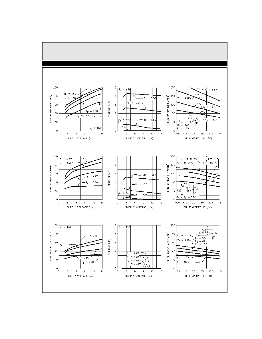
Typical Performance Curves
Non-Inverting Frequency
Response (Gain)
Non-Inverting Frequency
Response (Phase)
Frequency Response
for Various R
L
Inverting Frequency
Response (Gain)
Inverting Frequency
Response (Phase)
Frequency Response for
Various R
F
and R
G
3 dB Bandwidth vs
Temperature for A
V
= - 1
Peaking vs Supply Voltage
for A
V
= -1
3 dB Bandwidth vs Supply
Voltage for A
V
= -1
R
F
5
EL2160C
180MHz Current Feedback Amplifier
E
L
2
1
6
0
C
3 dB Bandwidth vs Supply
Voltage for A
V
= +1
Peaking vs Supply Voltage
for A
V
= +1
3 dB Bandwidth vs Temperature
for A
V
= +1
3 dB Bandwidth vs Temperature
for A
V
= +2
Peaking vs Supply Voltage
for A
V
= +2
3 dB Bandwidth vs Supply
Voltage for A
V
= +2
3 dB Bandwidth vs Supply
Voltage for A
V
= +10
Peaking vs Supply Voltage
for A
V
= +10
3 dB Bandwidth vs Temperature
for A
V
= +10

6
EL2160C
180MHz Current Feedback Amplifier
E
L
2
1
6
0
C
Frequency Response
for Various C
L
Frequency Response
for Various C
IN-
PSRR and CMRR
vs Frequency
2nd and 3rd Harmonic
Distortion vs Frequency
Transimpedance (R
OL
)
vs Frequency
Voltage and Current Noise
vs Frequency
Closed-Loop Output
Impedance vs Frequency
Transimpedance (R
OL
)
vs Die Temperature
7
EL2160C
180MHz Current Feedback Amplifier
E
L
2
1
6
0
C
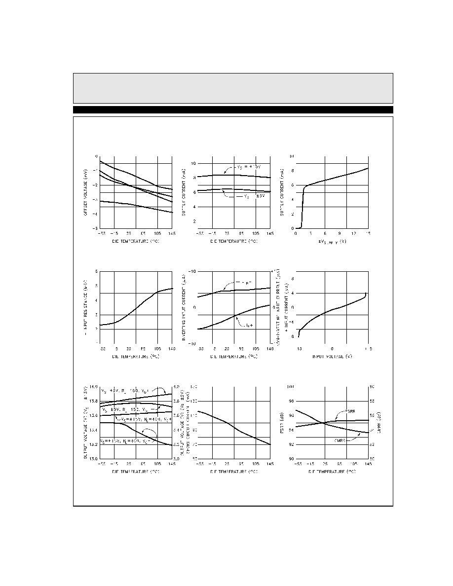
Offset Voltage
vs Die Temperature
(4 Samples)
Supply Current
vs Die Temperature
Supply Current
vs Supply Voltage
+Input Resistance
vs Die Temperature
Input Current
vs Die Temperature
+Input Bias Current
vs Input Voltage
Output Voltage Swing
vs Die Temperature
Short Circuit Current
vs Die Temperature
PSRR & CMRR
vs Die Temperature

8
EL2160C
180MHz Current Feedback Amplifier
E
L
2
1
6
0
C
Differential Gain
vs DC Input Voltage,
R
L
= 150
Differential Phase
vs DC Input Voltage,
R
L
= 150
Small Signal
Pulse Response
Differential Gain
vs DC Input Voltage,
R
L
= 500
Differential Phase
vs DC Input Voltage,
R
L
= 500
Large Signal
Pulse Response
Slew Rate
vs Supply Voltage
Slew Rate
vs Temperature
Settling Time
vs Settling Accuracy

9
EL2160C
180MHz Current Feedback Amplifier
E
L
2
1
6
0
C
Burn-In Circuit
Long Term Settling Error
0
25
50
75
100
125
150
85
Ambient Temperature (∞C)
1.6
1.4
1
0.8
0.6
0.4
0.2
0
1.2
P
o
w
e
r
D
i
s
s
i
p
a
t
i
o
n
(
W
)
Package Power Dissipation vs Ambient Temp.
JEDEC JESD51-3 Low Effective Thermal Conductivity Test Board
SO16 (0.300")
JA
=93∞C/W
SO8
JA
=160∞C/W
PDIP8
JA
=100∞C/W
781m
1.250
1.344
EL2160C

10
EL2160C
180MHz Current Feedback Amplifier
E
L
2
1
6
0
C
Differential Gain and Phase Test Circuit
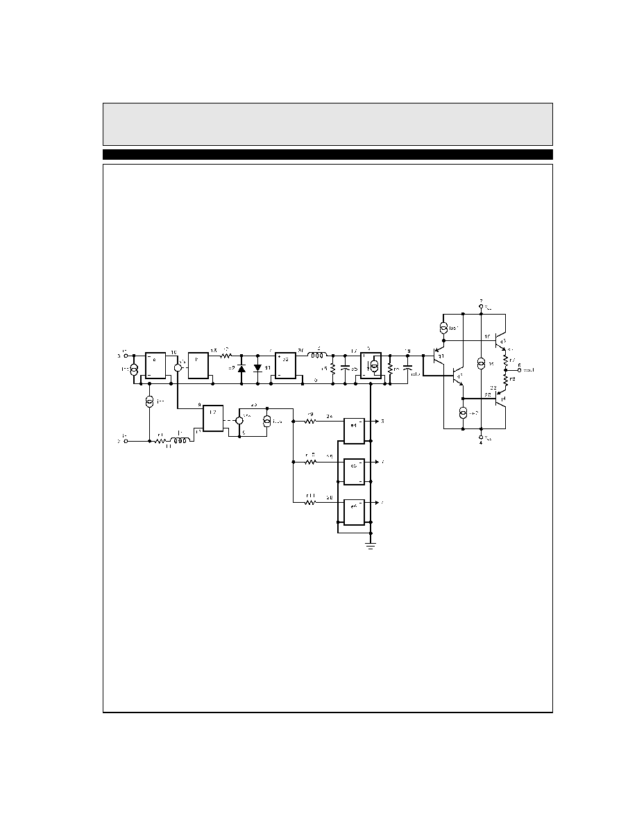
Simplified Schematic
(One Amplifier)

11
EL2160C
180MHz Current Feedback Amplifier
E
L
2
1
6
0
C
Applications Information
Product Description
The EL2160C is a current mode feedback amplifier that
offers wide bandwidth and good video specifications at a
moderately low supply current. It is built using Elantec's
proprietary complimentary bipolar process and is
offered in industry standard pin-outs. Due to the current
feedback architecture, the EL2160C closed-loop 3dB
bandwidth is dependent on the value of the feedback
resistor. First the desired bandwidth is selected by
choosing the feedback resistor, R
F
, and then the gain is
set by picking the gain resistor, R
G
. The curves at the
beginning of the Typical Performance Curves section
show the effect of varying both R
F
and R
G
. The 3dB
bandwidth is somewhat dependent on the power supply
voltage. As the supply voltage is decreased, internal
junction capacitances increase, causing a reduction in
closed loop bandwidth. To compensate for this, smaller
values of feedback resistor can be used at lower supply
voltages.
Power Supply Bypassing and Printed Circuit
Board Layout
As with any high frequency device, good printed circuit
board layout is necessary for optimum performance.
Ground plane construction is highly recommended.
Lead lengths should be as short as possible, below º.
The power supply pins must be well bypassed to reduce
the risk of oscillation. A 1.0µF tantalum capacitor in
parallel with a 0.01µF ceramic capacitor is adequate for
each supply pin.
For good AC performance, parasitic capacitances should
be kept to a minimum, especially at the inverting input
(see Capacitance at the Inverting Input section). This
implies keeping the ground plane away from this pin.
Carbon resistors are acceptable, while use of wire-
wound resistors should not be used because of their par-
asitic inductance. Similarly, capacitors should be low
inductance for best performance. Use of sockets, partic-
ularly for the SO package, should be avoided. Sockets
add parasitic inductance and capacitance which will
result in peaking and overshoot.
Capacitance at the Inverting Input
Due to the topology of the current feedback amplifier,
stray capacitance at the inverting input will affect the
AC and transient performance of the EL2160C when
operating in the non-inverting configuration. The char-
acteristic curve of gain vs. frequency with variations of
C
IN
- emphasizes this effect. The curve illustrates how
the bandwidth can be extended to beyond 200MHz with
some additional peaking with an additional 2pF of
capacitance at the V
IN
- pin for the case of A
V
= +2.
Higher values of capacitance will be required to obtain
similar effects at higher gains.
In the inverting gain mode, added capacitance at the
inverting input has little effect since this point is at a vir-
tual ground and stray capacitance is therefore not "seen"
by the amplifier.
Feedback Resistor Values
The EL2160C has been designed and specified with
R
F
=560
for A
V
= +2. This value of feedback resistor
yields extremely flat frequency response with little to no
peaking out to 130MHz. As is the case with all current
feedback amplifiers, wider bandwidth, at the expense of
slight peaking, can be obtained by reducing the value of
the feedback resistor. Inversely, larger values of feed-
back resistor will cause rolloff to occur at a lower
frequency. By reducing R
F
to 430
, bandwidth can be
extended to 170MHz with under 1dB of peaking. Fur-
ther reduction of R
F
to 360
increases the bandwidth to
195MHz with about 2.5dB of peaking. See the curves in
the Typical Performance Curves section which show
3dB bandwidth and peaking vs. frequency for various
feedback resistors and various supply voltages.
Bandwidth vs Temperature
Whereas many amplifier's supply current and conse-
quently 3dB bandwidth drop off at high temperature, the
EL2160C was designed to have little supply current
variations with temperature. An immediate benefit from
this is that the 3dB bandwidth does not drop off drasti-
cally with temperature. With V
S
= ±15V and A
V
= +2,
the bandwidth only varies from 150MHz to 110MHz
12
EL2160C
180MHz Current Feedback Amplifier
E
L
2
1
6
0
C
over the entire die junction temperature range of 0∞C < T
< 150∞C.
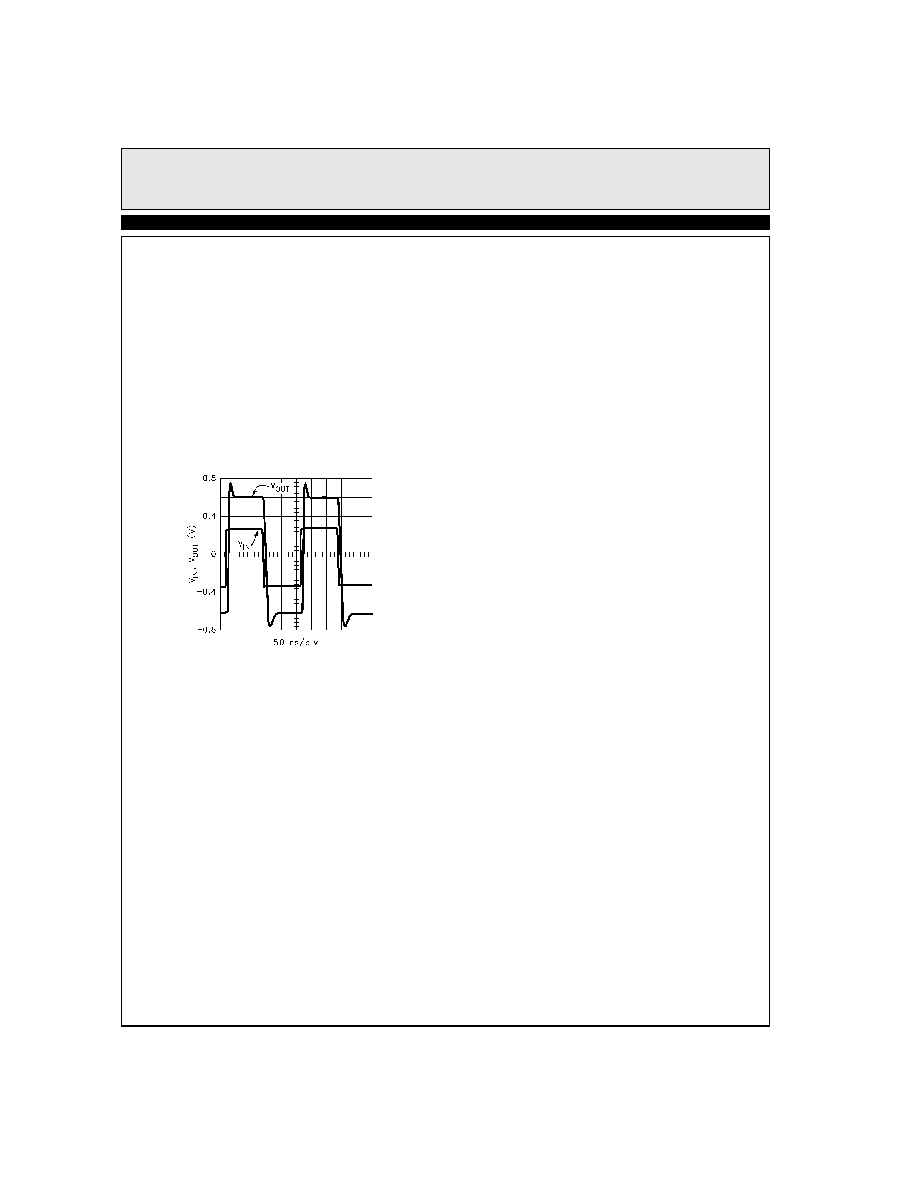
Supply Voltage Range
The EL2160C has been designed to operate with supply
voltages from ±2V to ±15V. Optimum bandwidth, slew
rate, and video characteristics are obtained at higher sup-
ply voltages. However, at ±2V supplies, the 3dB
bandwidth at A
V
= +2 is a respectable 70MHz. The fol-
lowing figure is an oscilloscope plot of the EL2160C at
±2V supplies, A
V
= +2, R
F
= R
G
= 560
, driving a load
of 150
, showing a clean ±600mV signal at the output.
If a single supply is desired, values from +4V to +30V
can be used as long as the input common mode range is
not exceeded. When using a single supply, be sure to
either 1) DC bias the inputs at an appropriate common
mode voltage and AC couple the signal, or 2) ensure the
driving signal is within the common mode range of the
EL2160C.
Settling Characteristics
The EL2160C offers superb settling characteristics to
0.1%, typically in the 35ns to 40ns range. There are no
aberrations created from the input stage which often
cause longer settling times in other current feedback
amplifiers. The EL2160C is not slew rate limited, there-
fore any size step up to ±10V gives approximately the
same settling time.
As can be seen from the Long Term Settling Error curve,
for A
V
= +1, there is approximately a 0.035% residual
which tails away to 0.01% in about 40µs. This is a ther-
mal settling error caused by a power dissipation
differential (before and after the voltage step). For A
V
=
-1, due to the inverting mode configuration, this tail does
not appear since the input stage does not experience the
large voltage change as in the non-inverting mode. With
A
V
= -1, 0.01% settling time is slightly greater than
100ns.
Power Dissipation
The EL2160C amplifier combines both high speed and
large output current drive capability at a moderate sup-
ply current in very small packages. It is possible to
exceed the maximum junction temperature allowed
under certain supply voltage, temperature, and loading
conditions. To ensure that the EL2160C remains within
its absolute maximum ratings, the following discussion
will help to avoid exceeding the maximum junction
temperature.
The maximum power dissipation allowed in a package is
determined by its thermal resistance and the amount of
temperature rise according to:
The maximum power dissipation actually produced by
an IC is the total quiescent supply current times the total
power supply voltage plus the power in the IC due to the
load, or:
where I
S
is the supply current. (To be more accurate, the
quiescent supply current flowing in the output driver
transistor should be subtracted from the first term
because, under loading and due to the class AB nature of
the output stage, the output driver current is now
included in the second term.)
In general, an amplifier's AC performance degrades at
higher operating temperature and lower supply current.
Unlike some amplifiers, the EL2160C maintains almost
constant supply current over temperature so that AC per-
formance is not degraded as much over the entire
operating temperature range. Of course, this increase in
performance doesn't come for free. Since the current has
increased, supply voltages must be limited so that maxi-
mum power ratings are not exceeded.
P
DMAX
T
JMAX
T
AMAX
≠
JA
---------------------------------------------
=
P
DMAX
2 V
S
V
(
S
V
OUT
)
V
OUT
R
L
---------------
◊
≠
+
◊
=

13
EL2160C
180MHz Current Feedback Amplifier
E
L
2
1
6
0
C
The EL2160C consumes typically 8.5mA and maximum
11.0mA. The worst case power in an IC occurs when the
output voltage is at half supply, if it can go that far, or its
maximum values if it cannot reach half supply. If we set
the two P
DMAX
equations equal to each other, and solve
for V
S
, we can get a family of curves for various loads
and output voltages according to:
The following curves show supply voltage (±V
S
) vs
R
LOAD
for various output voltage swings for the 2 dif-
ferent packages. The curves assume worst case
conditions of T
A
= +85∞C and I
S
= 11mA.
The curves do not include heat removal or forcing air, or
the simple fact that the package will probably be
attached to a circuit board, which can also provide some
form of heat removal. Larger temperature and voltage
ranges are possible with heat removal and forcing air
past the part.
Current Limit
The EL2160C has an internal current limit that protects
the circuit in the event of the output being shorted to
ground. This limit is set at 100mA nominally and
reduces with junction temperature. At a junction temper-
ature of 150∞C, the current limits at about 65mA. If the
output is shorted to ground, the power dissipation could
be well over 1W. Heat removal is required in order for
the EL2160C to survive an indefinite short.
Driving Cables and Capacitive Loads
When used as a cable driver, double termination is
always recommended for reflection-free performance.
For those applications, the back termination series resis-
tor will decouple the EL2160C from the capacitive cable
and allow extensive capacitive drive. However, other
applications may have high capacitive loads without ter-
mination resistors. In these applications, an additional
small value (5
≠50
) resistor in series with the output
will eliminate most peaking. The gain resistor, R
G
, can
be chosen to make up for the gain loss created by this
additional series resistor at the output.
V
S
R
L
T
MAX
-T
AMAX
(
)
◊
JA
----------------------------------------------------------
V
OUT
(
)
2
(
I
S
R
L
)
V
OUT
+
◊
◊
[
]
˜
+
=
Supply Voltage vs R
LOAD
for Various V
OUT
(8-Pin SO Package)
Supply Voltage vs R
LOAD
for
Various V
OUT
(PDIP Package)

14
EL2160C
180MHz Current Feedback Amplifier
E
L
2
1
6
0
C
EL2160C Macromodel
* Revision A, November 1993
* AC Characteristics used C
IN
- (pin 2) = 1 pF; R
F
= 560
* Connections: +input
* | -input
* | | +Vsupply
* | | | -Vsupply
* | | | | output
* | | | | |
.subckt EL2160C/EL 3 2 7 4 6
*
* Input Stage
*
e1 10 0 3 0 1.0
vis 10 9 0V
h2 9 12 vxx 1.0
r1 2 11 130
l1 11 12 25nH
iinp 3 0 0.5µA
iinm 2 0 5µA
r12 3 0 2Meg
*
* Slew Rate Limiting
*
h1 13 0 vis 600
r2 13 14 1K
d1 14 0 dclamp
d2 0 14 dclamp
*
* High Frequency Pole
*
*e2 30 0 14 0 0.00166666666
l3 30 17 0.43µH
c5 17 0 0.27pF
r5 17 0 500
*
* Transimpedance Stage
*
g1 0 18 17 0 1.0
ro1 18 0 2Meg
cdp 18 0 2.285pF
*
* Output Stage
*
q1 4 18 19 qp
q2 7 18 20 qn
q3 7 19 21 qn
q4 4 20 22 qp
r7 21 6 4
r8 22 6 4
ios1 7 19 2mA
ios2 20 4 2mA
*
* Supply Current
*
ips 7 4 3mA
*
* Error Terms
*
ivos 0 23 2mA
vxx 23 0 0V
e4 24 0 3 0 1.0
e5 25 0 7 0 1.0
15
EL2160C
180MHz Current Feedback Amplifier
E
L
2
1
6
0
C
e6 26 0 4 0 1.0
r9 24 23 562
r10 25 23 1K
r11 26 23 1K
*
* Models
*
.model qn npn (is=5e-15 bf=100 tf=0.1ns)
.model qp pnp (is=5e-15 bf=100 tf=0.1ns)
.model dclamp d (is=1e-30 ibv=0.266 bv=2.24 n=4)
.ends
EL2160C Macromodel

16
EL2160C
180MHz Current Feedback Amplifier
E
L
2
1
6
0
C

17
EL2160C
180MHz Current Feedback Amplifier
E
L
2
1
6
0
C
18
EL2160C
180MHz Current Feedback Amplifier
E
L
2
1
6
0
C
General Disclaimer
Specifications contained in this data sheet are in effect as of the publication date shown. Elantec, Inc. reserves the right to make changes in the cir-
cuitry or specifications contained herein at any time without notice. Elantec, Inc. assumes no responsibility for the use of any circuits described
herein and makes no representations that they are free from patent infringement.
WARNING - Life Support Policy
Elantec, Inc. products are not authorized for and should not be used
within Life Support Systems without the specific written consent of
Elantec, Inc. Life Support systems are equipment intended to sup-
port or sustain life and whose failure to perform when properly used
in accordance with instructions provided can be reasonably
expected to result in significant personal injury or death. Users con-
templating application of Elantec, Inc. Products in Life Support
Systems are requested to contact Elantec, Inc. factory headquarters
to establish suitable terms & conditions for these applications. Elan-
tec, Inc.'s warranty is limited to replacement of defective
components and does not cover injury to persons or property or
other consequential damages.
S
e
p
t
e
m
b
e
r
2
6
,
2
0
0
1
Printed in U.S.A.
Elantec Semiconductor, Inc.
675 Trade Zone Blvd.
Milpitas, CA 95035
Telephone: (408) 945-1323
(888) ELANTEC
Fax:
(408) 945-9305
European Office: +44-118-977-6020
Japan Technical Center: +81-45-682-5820