 | –≠–ª–µ–∫—Ç—Ä–æ–Ω–Ω—ã–π –∫–æ–º–ø–æ–Ω–µ–Ω—Ç: EL2244CN | –°–∫–∞—á–∞—Ç—å:  PDF PDF  ZIP ZIP |
Note: All information contained in this data sheet has been carefully checked and is believed to be accurate as of the date of publication; however, this data sheet cannot be a "controlled document". Current revisions, if any, to these
specifications are maintained at the factory and are available upon your request. We recommend checking the revision level before finalization of your design documentation.
© 2001 Elantec Semiconductor, Inc.
E
L
2
2
4
4
C
,
E
L
2
4
4
4
C
General Description
The EL2244C/EL2444C are dual and quad versions of the popular
EL2044C. They are high speed, low power, low cost monolithic oper-
ational amplifiers built on Elantec's proprietary complementary
bipolar process. The EL2244C/EL2444C are unity-gain stable and
feature a 325V/µs slew rate and 120MHz gain-bandwidth product
while requiring only 5.2mA of supply current per amplifier.
The power supply operating range of the EL2244C/EL2444C is from
±18V down to as little as ±2V. For single-supply operation, the
EL2244C/EL2444C operate from 36V down to as little as 2.5V. The
excellent power supply operating range of the EL2244C/EL2444C
makes them an obvious choice for applications on a single +5V or
+3V supply.
The EL2244C/EL2444C also feature an extremely wide output volt-
age swing of ±13.6V with V
S
= ±15V and R
L
= 1000
. At ±5V,
output voltage swing is a wide ±3.8V with R
L
= 500
and ±3.2V with
R
L
= 150
. Furthermore, for single-supply operation at +5V, output
voltage swing is an excellent 0.3V to 3.8V with R
L
= 500
.
At a gain of +1, the EL2244C/EL2444C have a -3dB bandwidth of
120MHz with a phase margin of 50∞. They can drive unlimited load
capacitance, and because of their conventional voltage-feedback
topology, the EL2244C/EL2444C allow the use of reactive or non-lin-
ear elements in their feedback network. This versatility combined with
l o w c o s t a n d 7 5 m A o f o u t p u t - c u r r e n t d r i v e m a k e t h e
EL2244C/EL2444C an ideal choice for price-sensitive applications
requiring low power and high speed.
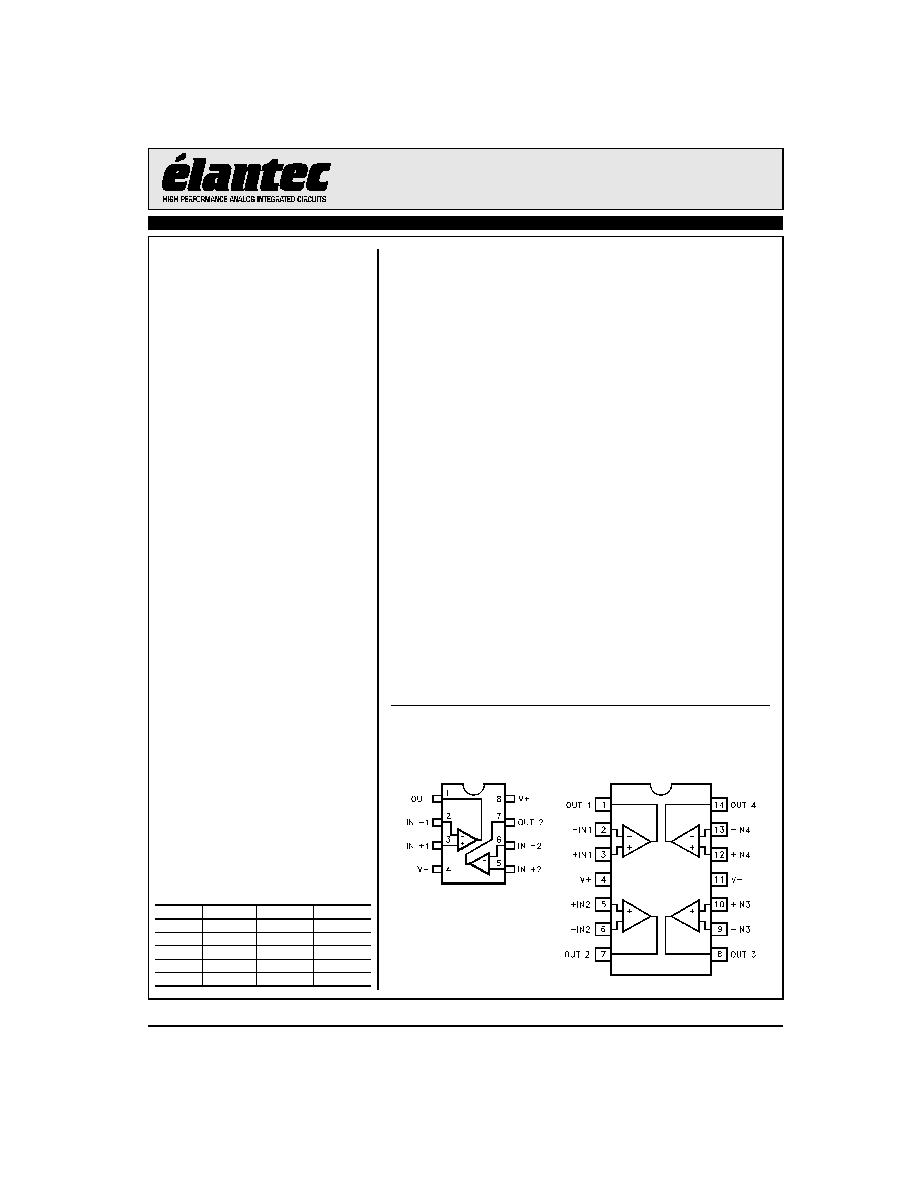
Connection Diagrams
EL2244CN/CS
Dual
EL2444CN/CS
Quad
Features
∑ 120MHz gain-bandwidth product
∑ Unity-gain stable
∑ Low supply current (per amplifier)
- 5.2mA at V
S
= ±15V
∑ Wide supply range - ±2V to ±18V
dual-supply, 2.5V to 36V single-
supply
∑ High slew rate - 325V/µs
∑ Fast settling - 80ns to 0.1% for a
10V step
∑ Low differential gain - 0.04% at
A
V
= +2, R
L
= 150æ
∑ Low differential phase - 0.15∞ at
A
V
= +2, R
L
= 150
∑ Stable w/ unlimited capacitive load
∑ Wide output voltage swing -
±13.6V with V
S
= ±15V, R
L
=
1000
,
3.8V/0.3V with V
S
= +5V,
R
L
= 500
∑ Low cost, enhanced replacement
for the AD827
andLT1229/LT1230
Applications
∑ Video amplifier
∑ Single-supply amplifier
∑ Active filters/integrators
∑ High-speed sample-and-hold
∑ High-speed signal processing
∑ ADC/DAC buffer
∑ Pulse/RF amplifier
∑ Pin diode receiver
∑ Log amplifier
∑ Photo multiplier amplifier
∑ Difference amplifier
Ordering Information
Part No.
Temp. Range
Package
Outline #
EL2244CN
-40∞C to +85∞C
8-Pin P-DIP
MDP0031
EL2244CS
-40∞C to +85∞C
8-Lead SO
MDP0027
EL2444CN
-40∞C to +85∞C
14-Pin P-DIP
MDP0031
EL2444CS
-40∞C to +85∞C
14-Lead SO
MDP0027
EL2444CM
-40∞C to +85∞C
16-Lead SOL
MDP0027
EL2244C, EL2444C
Dual/Quad Low-Power 120MHz Unity-Gain Stable Op Amp
S
e
p
t
e
m
b
e
r
2
6
,
2
0
0
1
2
EL2244C, EL2444C
Dual/Quad Low-Power 120MHz Unity-Gain Stable Op Amp
E
L
2
2
4
4
C
,
E
L
2
4
4
4
C
Absolute Maximum Ratings
(T
A
= 25 ∞C)
Supply Voltage (V
S
)
±18V or 36V
Peak Output Current (I
OP
)
Short-Circuit Protected
Output Short-Circuit Duration
Infinite
A heat-sink is required to keep junction temperature
below absolute maximum when an output is shorted.
Input Voltage (V
IN)
±V
S
Differential Input Voltage (dV
IN
)
±10V
Power Dissipation (P
D
)
See Curves
Operating Temperature Range (T
A
)
-40∞C to +85∞C
Operating Junction Temperature (T
J
)
150∞C
Storage Temperature (T
ST
)
-65∞C to +150∞C
Important Note:
All parameters having Min/Max specifications are guaranteed. Typ values are for information purposes only. Unless otherwise noted, all tests are at the
specified temperature and are pulsed tests, therefore: T
J
= T
C
= T
A
.
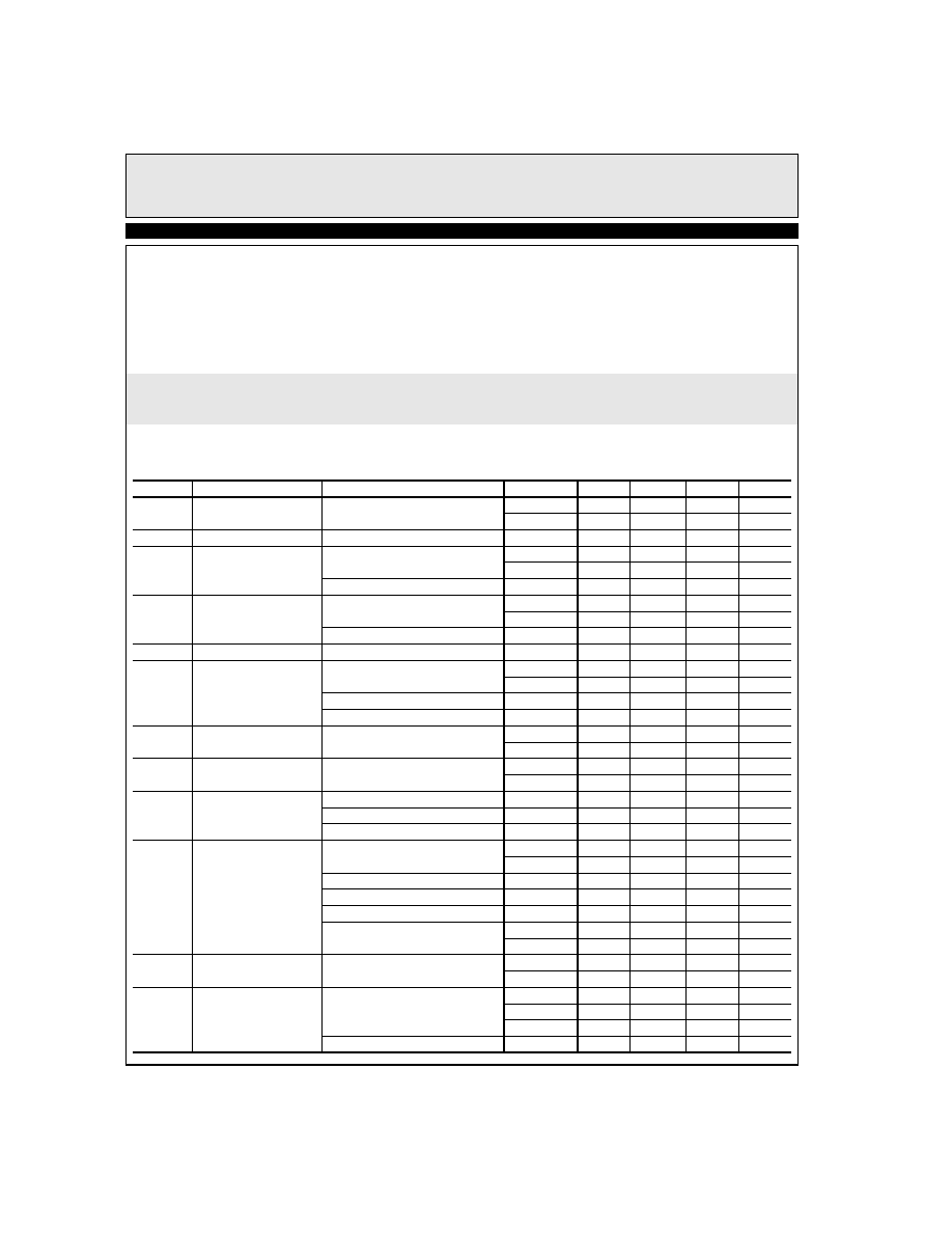
DC Electrical Characteristics
V
S
= ±15V, R
L
= 1000
, unless otherwise specified
Parameter
Description
Condition
Temp
Min
Typ
Max
Unit
V
OS
Input Offset
Voltage
V
S
= ±15V
25∞C
0.5
4.0
mV
T
MIN
, T
MAX
9.0
mV
TCV
OS
Average Offset Voltage Drift
[1]
All
10.0
µV/∞C
I
B
Input Bias
Current
V
S
= ±15V
25∞C
2.8
8.2
µA
T
MIN
, T
MAX
11.2
µA
V
S
= ±5V
25∞C
2.8
µA
I
OS
Input Offset
Current
V
S
= ±15V
25∞C
50
300
nA
T
MIN
, T
MAX
500
nA
V
S
= ±5V
25∞C
50
nA
TCI
OS
Average Offset Current Drift
[1]
All
0.3
nA/∞C
A
VOL
Open-Loop Gain
V
S
= ±15V,V
OUT
= ±10V, R
L
= 1000
25∞C
800
1500
V/V
T
MIN
, T
MAX
600
V/V
V
S
= ±5V, V
OUT
= ±2.5V, R
L
= 500
25∞C
1200
V/V
V
S
= ±5V, V
OUT
= ±2.5V, R
L
= 150
25∞C
1000
V/V
PSRR
Power Supply
Rejection Ratio
V
S
= ±5V to ±15V
25∞C
65
80
dB
T
MIN
, T
MAX
60
dB
CMRR
Common-Mode
Rejection Ratio
V
CM
= ±12V, V
OUT
= 0V
25∞C
70
90
dB
T
MIN
, T
MAX
70
dB
CMIR
Common-Mode
Input Range
V
S
= ±15V
25∞C
±14.0
V
V
S
= ±5V
25∞C
±4.2
V
V
S
= +5V
25∞C
4.2/0.1
V
V
OUT
Output Voltage
Swing
V
S
= ±15V, R
L
= 1000
25∞C
±13.4
±13.6
V
T
MIN
, T
MAX
±13.1
V
V
S
= ±15V, R
L
= 500
25∞C
±12.0
±13.4
V
V
S
= ±5V, R
L
= 500
25∞C
±3.4
±3.8
V
V
S
= ±5V, R
L
= 150
25∞C
±3.2
V
V
S
= +5V, R
L
= 500
25∞C
3.6/0.4
3.8/0.3
V
T
MIN
, T
MAX
3.5/0.5
V
I
SC
Output Short
Circuit Current
25∞C
40
75
mA
T
MIN
, T
MAX
35
mA
I
S
Supply Current
(Per Amplifier)
V
S
= ±15V, No Load
25∞C
5.2
7
mA
T
MIN
7.6
mA
T
MAX
7.6
mA
V
S
= ±5V, No Load
25∞C
5.0
mA
3
EL2244C, EL2444C
Dual/Quad Low-Power 120MHz Unity-Gain Stable Op Amp
E
L
2
2
4
4
C
,
E
L
2
4
4
4
C
R
IN
Input Resistance
Differential
25∞C
150
k
Common-Mode
25∞C
15
M
C
IN
Input Capacitance
A
V
= +1@ 10MHz
25∞C
1.0
pF
R
OUT
Output Resistance
A
V
= +1
25∞C
50
m
PSOR
Power-Supply
Operating Range
Dual-Supply
25∞C
±2.0
±18.0
V
Single-Supply
25∞C
2.5
36.0
V
1. Measured from T
MIN
to T
MAX
.
DC Electrical Characteristics (Continued)
V
S
= ±15V, R
L
= 1000
, unless otherwise specified
Parameter
Description
Condition
Temp
Min
Typ
Max
Unit
4
EL2244C, EL2444C
Dual/Quad Low-Power 120MHz Unity-Gain Stable Op Amp
E
L
2
2
4
4
C
,
E
L
2
4
4
4
C
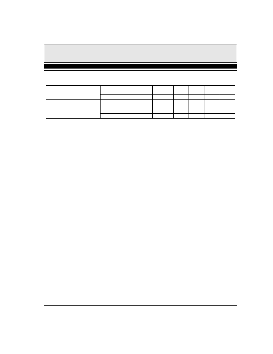
Closed-Loop AC Electrical Characteristics
V
S
= ±15V, A
V
= +1, R
L
= 1000
unless otherwise specified
Parameter
Description
Condition
Temp
Min
Typ
Max
Unit
BW
-3dB Bandwidth
(V
OUT
= 0.4V
PP
)
V
S
= ±15V, A
V
= +1
25∞C
120
MHz
V
S
= ±15V, A
V
= -1
25∞C
60
MHz
V
S
= ±15V, A
V
= +2
25∞C
60
MHz
V
S
= ±15V, A
V
= +5
25∞C
12
MHz
V
S
= ±15V, A
V
= +10
25∞C
6
MHz
V
S
= ±5V, A
V
= +1
25∞C
80
MHz
GBWP
Gain-Bandwidth Product
V
S
= ±15V
25∞C
60
MHz
V
S
= ±5V
25∞C
45
MHz
PM
Phase Margin
R
L
= 1 kæ, C
L
= 10pF
25∞C
50
∞
CS
Channel Separation
f = 5MHz
25∞C
85
dB
SR
Slew Rate
[1]
V
S
= ±15V, R
L
= 1000
25∞C
250
325
V/µs
V
S
= ±5V, R
L
= 500
25∞C
200
V/µs
FPBW
Full-Power Bandwidth
[2]
V
S
= ±15V
25∞C
4.0
5.2
MHz
V
S
= ±5V
25∞C
12.7
MHz
t
r
, t
f
Rise Time, Fall Time
0.1V Step
25∞C
3.0
ns
OS
Overshoot
0.1V Step
25∞C
20
%
t
PD
Propagation Delay
25∞C
2.5
ns
t
s
Settling to +0.1%
(A
V
= +1)
V
S
= ±15V, 10V Step
25∞C
80
ns
V
S
= ±5V, 5V Step
25∞C
60
ns
dG
Differential Gain
[3]
NTSC/PAL
25∞C
0.04
%
dP
Differential Phase
[3]
NTSC/PAL
25∞C
0.15
∞
eN
Input Noise Voltage
10kHz
25∞C
15.0
nV
Hz
iN
Input Noise Current
10kHz
25∞C
1.50
pA
Hz
CI STAB
Load Capacitance Stability
A
V
= +1
25∞C
Infinite
pF
1. Slew rate is measured on rising edge
2. For V
S
= ±15V, V
OUT
= 20V
PP
. For V
S
= ±5V, V
OUT
= 5V
PP
. Full-power bandwidth is based on slew rate measurement using: FPBW = SR/(2
*
Vpeak).
3. Video Performance measured at V
S
= ±15V, A
V
= +2 with 2 times normal video level across R
L
= 150
. This corresponds to standard video levels
across a back-terminated 75
load. For other values of R
L
, see curves.
5
EL2244C, EL2444C
Dual/Quad Low-Power 120MHz Unity-Gain Stable Op Amp
E
L
2
2
4
4
C
,
E
L
2
4
4
4
C
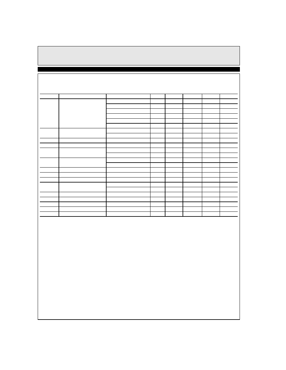
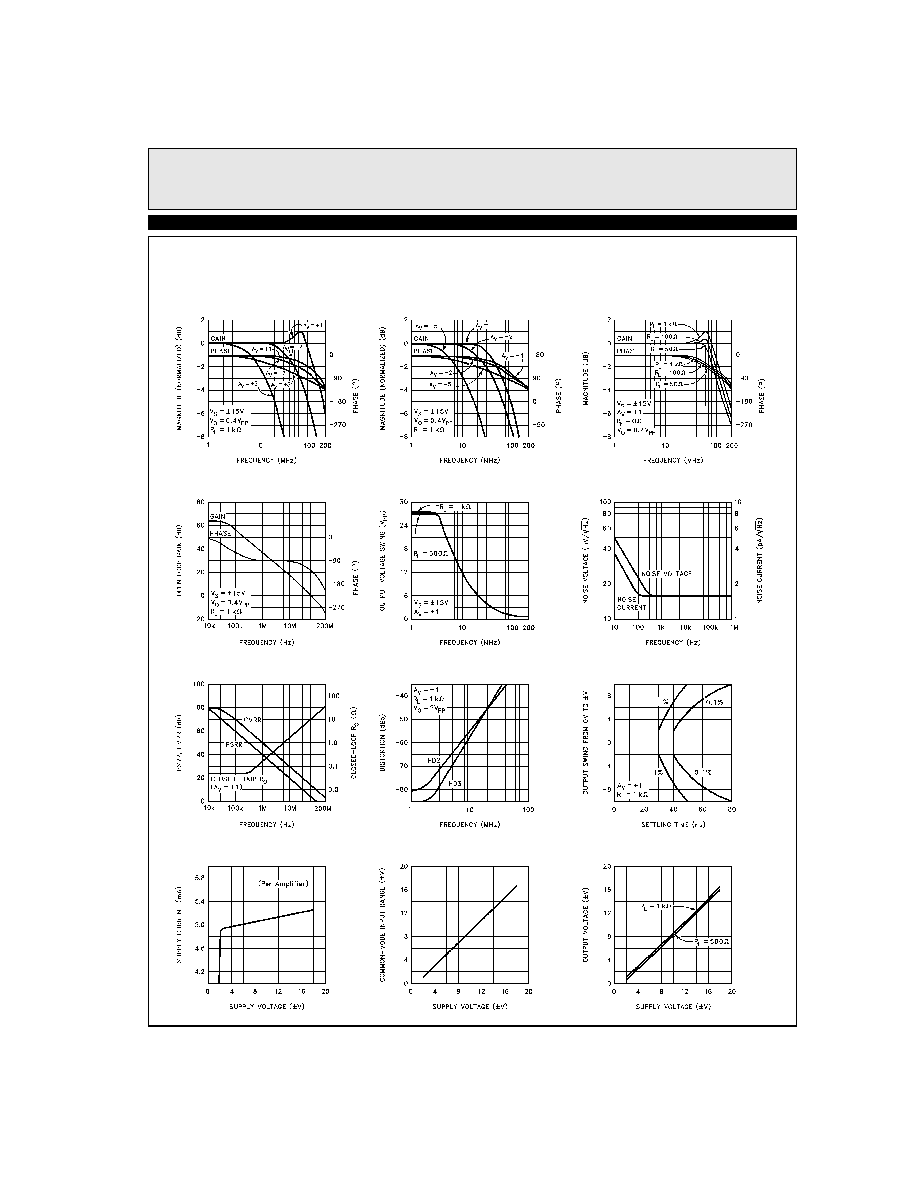
Typical Performance Curves
Non-Inverting
Frequency Response
Inverting Frequency Response
Frequency Response for
Various Load Resistances
Equivalent Input Noise
Settling Time vs
Output Voltage Change
2nd and 3rd Harmonic
Distortion vs Frequency
CMRR, PSRR and Closed-Loop
Output Resistance vs Frequency
Open-Loop Gain and
Phase vs Frequency
Output Voltage Swing
vs Frequency
Common-Mode Input Range
vs Supply Voltage
Supply Current vs
Supply Voltage
Output Voltage Range
vs Supply Voltage