EL2252C
December
1995
Rev
E
EL2252C
Dual 50 MHz Comparator Pin Receiver
Note All information contained in this data sheet has been carefully checked and is believed to be accurate as of the date of publication however this data sheet cannot be a ``controlled document'' Current revisions if any to these
specifications are maintained at the factory and are available upon your request We recommend checking the revision level before finalization of your design documentation Patent pending
1995 Elantec Inc
Features
Fast response
7 ns
Inputs tolerate large overdrives
with no speed nor bias current
penalties
Propagation delay is relatively
constant with variations of input
Slew Rate overdrive
temperature and supply voltage
Output provides proper CMOS or
TTL logic levels
Hysteresis is available on-chip
Large voltage gain
8000 V V
Not oscillation-prone
Can detect 4 ns glitches
MIL-STD-883 Rev C compliant
Applications
Pin receiver for automatic test
equipment
Data communications line
receiver
Frequency counter input
Pulse squarer
Ordering Information
Part No
Temp Range
Package
Outline
EL2252CN
0 C to
a
75 C
14-Pin P-DIP
MDP0031
EL2252CM
0 C to
a
75 C
20-Lead SOL
MDP0027
General Description
The EL2252 dual comparator replaces the traditional input
buffer
a
attenuator
a
ECL comparator
a
ECL to TTL transla-
tor circuit blocks used in digital equipment The EL2252 pro-
vides a quick 7 ns propagation delay while complying with
g
10V inputs Input accuracy and propagation delay is main-
tained even with input signal Slew Rates as great as 4000 V
ms
The EL2252 can run on supplies as low as
b
5 2V and
a
9V and
comply with ECL and CMOS inputs or use supplies as great as
g
18V for much greater input range
The EL2252 has a
TTL pin which when grounded restricts
the output V
OH
to a TTL swing to minimize propagation delay
When left open the output V
OH
increases to a valid CMOS
level
The comparators are well behaved and have little tendency to
oscillate over a variety of input and output source and load
impedances They do not oscillate even when the inputs are
held in the linear range of the device To improve output stabili-
ty in the presence of input noise an internal 60 mV of hystere-
sis is available by connecting the HYS pin to V
b
Elantec's products and facilities comply with MIL-I-45208A
and other applicable quality specifications For information on
Elantec's processing see Elantec document QRA-1 ``Elantec's
Processing Monolithic Integrated Circuits
''
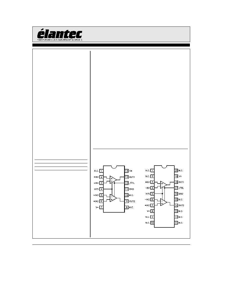
Connection Diagrams
14-Pin DIP
20-Pin SOL
2252 � 1
Top View
2252 � 2
Top View
EL2252C
Dual 50 MHz Comparator Pin Receiver
Absolute Maximum Ratings
(T
A
e
25 C)
Voltage between V
a
and V
b
36V
Voltage at V
a
18V
Voltage between
b
IN and
a
IN pins
36V
Output Current
12 mA
Current into
a
IN
b
IN HYS
or TTL
5 mA
Internal Power Dissipation
See Curves
Operating Ambient Temperature Range
b
25 C to
a
85 C
Operating Junction Temperature
150 C
Storage Temperature Range
b
65 to
a
150C
Important Note
All parameters having Min Max specifications are guaranteed The Test Level column indicates the specific device testing actually
performed during production and Quality inspection Elantec performs most electrical tests using modern high-speed automatic test
equipment specifically the LTX77 Series system Unless otherwise noted all tests are pulsed tests therefore T
J
e
T
C
e
T
A
Test Level
Test Procedure
I
100% production tested and QA sample tested per QA test plan QCX0002
II
100% production tested at T
A
e
25 C and QA sample tested at T
A
e
25 C
T
MAX
and T
MIN
per QA test plan QCX0002
III
QA sample tested per QA test plan QCX0002
IV
Parameter is guaranteed (but not tested) by Design and Characterization Data
V
Parameter is typical value at T
A
e
25 C for information purposes only
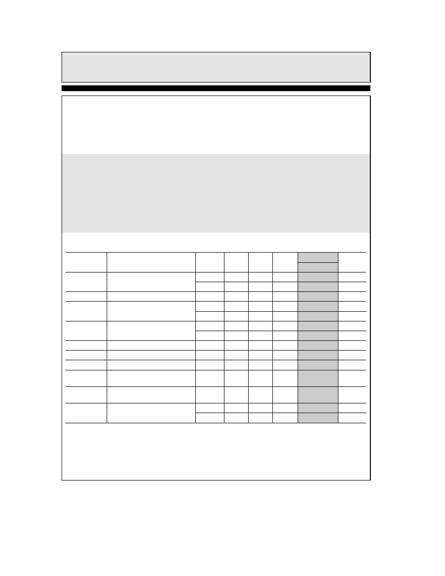
DC Electrical Characteristics
V
S
e
g
15V HYS and TTL grounded T
A
e
25 C unless otherwise specified
Parameter
Description
Temp
Min
Typ
Max
Test Level
Units
EL2252C
V
OS
Input Offset Voltage
25 C
1
9
I
mV
Full
13
III
mV
TCV
OS
Average Offset Voltage Drift
Full
7
V
mV C
I
B
Input Bias Current at Null
25 C
6
16
I
mA
Full
21
III
mA
I
OS
Input Offset Current
25 C
0 2
1
I
mA
Full
2
III
mA
R
IN
diff
Input Differential Resistance
25 C
30
V
k
X
R
IN
comm
Input Common-Mode Resistance
25 C
10
V
M
X
C
IN
Input Capacitance
25 C
2
V
pF
V
CM
a
Positive Common-Mode
Full
10
13
II
V
Input Range
V
CM
b
Negative Common-Mode
Full
b
9
b
12
II
V
Input Range
A
VOL
Large Signal Voltage Gain
25 C
4000
8000
I
V V
V
O
e
0 8V to 2 0V
Full
3000
III
V V
2
TD
is
33in
EL2252C
Dual 50 MHz Comparator Pin Receiver
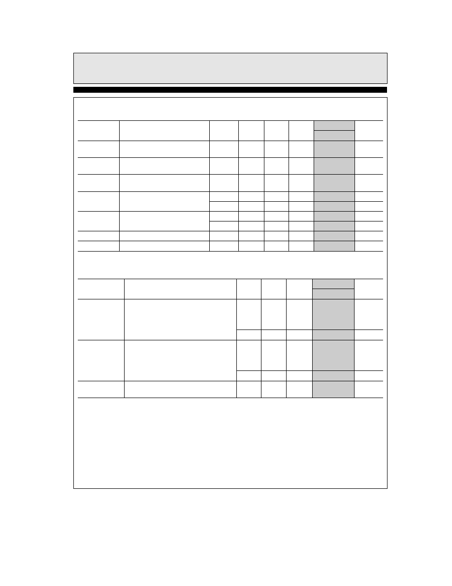
DC Electrical Characteristics
V
S
e
g
15V HYS and TTL grounded T
A
e
25 C unless otherwise specified
Contd
Parameter
Description
Temp
Min
Typ
Max
Test Level
Units
EL2252C
CMRR
Common-Mode Rejection Ratio
Full
70
95
II
dB
(Note 1)
PSRR
Power-Supply Rejection Ratio
Full
70
90
II
dB
(Note 2)
V
HYS
Peak-to-Peak Input Hysteresis
25 C
60
V
mV
with HYS connected to V
b
V
OH
High Level Output CMOS Mode
Full
4 0
4 6
5 1
II
V
TTL Mode
Full
2 4
2 7
3 2
II
V
V
OL
Low Level Output I1
e
0
Full
b
0 2
0 2
0 8
II
V
I1
e
5 mA
Full
b
0 2
0 4
0 8
II
V
I
S
a
Positive Supply Current
Full
16
19
II
mA
I
S
b
Negative Supply Current
Full
17
20
II
mA
AC Electrical Characteristics
V
S
e
g
15V C
L
e
10 pF T
A
e
25 C TTL output threshold is 1 4V CMOS output threshold is 2 5V unless otherwise specified
Parameter
Description
Min
Typ
Max
Test Level
Units
EL2252C
T
PDa
T
PDb
Input to Output Propagation Delay
0
k
V
IN
k
5V 500 mV Overdrive
6
9
III
ns
2000 V
ms Input Slew Rate
TTL Output Swing
CMOS Output Swing
8
V
ns
T
PDa
T
PDb
Input to Output Propagation Delay
b
2V
k
V
IN
k
b
1V 500 mV Overdrive
5
9
III
ns
2 ns Input Rise Time
TTL Output Swing
CMOS Output Swing
9
V
ns
T
PDSYM
Propagation Delay Change between
1 25
V
ns
Positive and Negative Input Slopes
Note 1 Two tests are performed with V
CM
e
0V to
b
9V and V
CM
e
0V to 10V
Note 2 Two tests are performed with V
a e
15V V
b
changed from
b
10V to
b
15V
V
b e b
15V V
a
changed from 10V to 15V
3
TD
is
25in
TD
is
22in

EL2252C
Dual 50 MHz Comparator Pin Receiver
AC Test Circuit
2252 � 3
Burn-In Circuit
2252 � 4
4

EL2252C
Dual 50 MHz Comparator Pin Receiver
Typical Performance Curves
vs Small Overdrives
Input Bias Current
vs Large Overdrives
Input Bias Current
Temperature
Inputs Balanced
Bias Current vs
vs Temperature
Input Hysteresis Voltage
2252 � 5
Input Output Transfer
Function
HYS Open
2252 � 6
Input Output Transfer
Function
HYS Connected to V
2252 � 7
5

EL2252C
Dual 50 MHz Comparator Pin Receiver
Typical Performance Curves
Contd
Supply Voltage
Supply Current vs
Supply Current vs Temperature
(V
S
e
g
15V)
2252 � 8
Output Delay
0 5V Overdrive
2252 � 9
Output Delay
0 5V Overdrive
2252 � 10
Output with 50 MHz CMOS Input
2252 � 11
Output with 50 MHz ECL Input
2252 � 12
6

EL2252C
Dual 50 MHz Comparator Pin Receiver
Typical Performance Curves
Contd
4 ns TTL Glitch Detection
2252 � 13
Gain vs Frequency
Propagation Delay vs
Temperature CMOS Input
Propagation Delay vs
Temperature ECL Input
Overdrive CMOS Input
Propagation Delay vs
Input Slew Rate CMOS Input
Propagation Delay vs
2252 � 14
7
EL2252C
Dual 50 MHz Comparator Pin Receiver
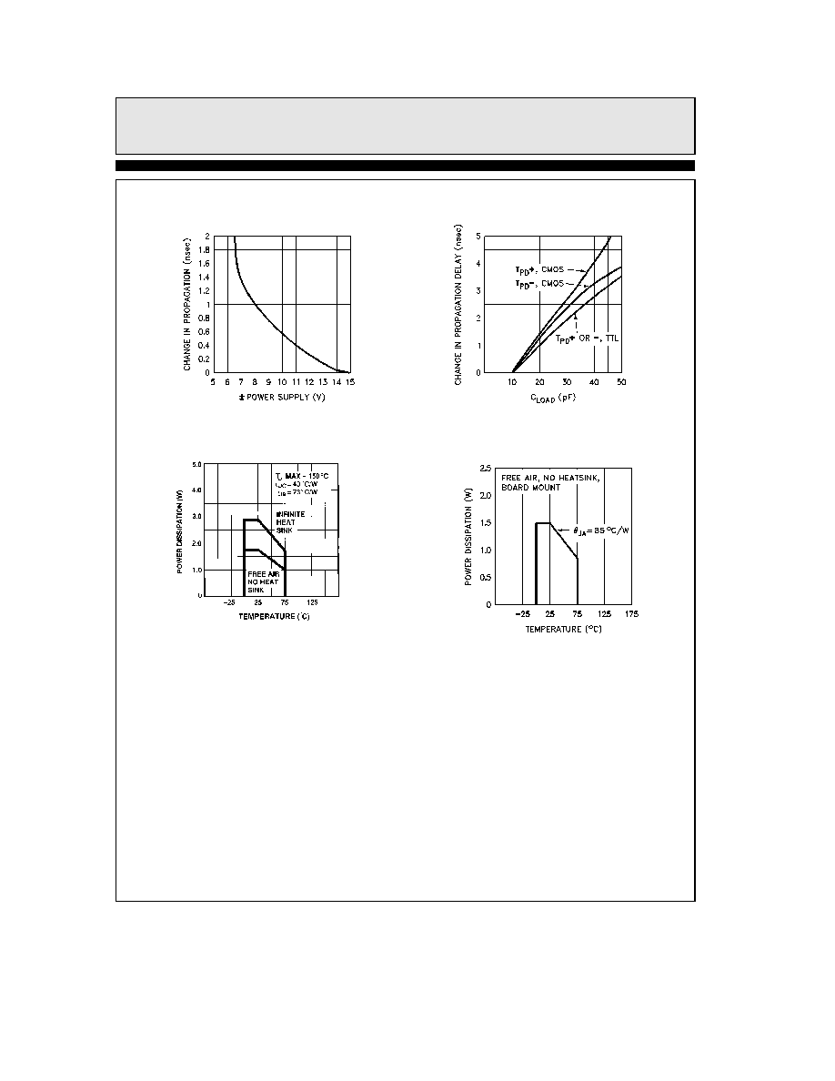
Typical Performance Curves
Contd
Power Supply Voltage
Propagation Delay vs
Propagation Delay vs
Load Capacitance
2252 � 15
14-Lead Plastic DIP
Maximum Power Dissipation
vs Ambient Temperature
2252 � 16
20-Lead SOL
Maximum Power Dissipation
vs Ambient Temperature
2252 � 18
8

EL2252C
Dual 50 MHz Comparator Pin Receiver
Simplified Schematic
One Comparator
2252 � 19
Applications Information
The EL2252 is very easy to use and is relatively
oscillation-free but a few items must be attend-
ed The first is that both supplies should be by-
passed closely 1
mF tantalums are very good and
no additional smaller capacitors are necessary
The EL2252 requires V
b
to be at least 5V to pre-
serve AC performance V
a
must be at least 6V
for a TTL output swing 8V for CMOS outputs
The input voltage range will be referred to the
more positive of the two inputs That is bringing
an input as negative as V
b
will not cause prob-
lems it's the other input's level that must be con-
sidered The typical input range is
a
13
b
12V
when the supplies are
g
15V This range dimin-
ishes over temperature and varies with process-
ing it is wise to set power supplies such that V
a
is 5V more positive than the most positive input
signal and V
b
more negative than 6V below the
most negative input
g
12V supplies will easily
encompass all CMOS and ECL logic inputs If
the input exceeds the device's common-mode in-
put capability
the EL2252 propagation delay
and input bias current will increase Fault cur-
rents will occur with inputs a diode below V
b
or
above V
a
No damage nor V
OS
shift will occur
even when fault currents within the absolute
maximum ratings
9

EL2252C
Dual 50 MHz Comparator Pin Receiver
Applications Information
Contd
One of the few ways in which oscillations can be
induced is by connecting a high-Q reactive source
impedance to the EL2252 inputs Such sources
are long wires and unterminated coaxial lines
The source impedance should be de-Q'ed One
method is to connect a series resistor to the
EL2252 input of around 100
X value More resist-
ance will calm the system more effectively but at
the expense of comparator response time Anoth-
er method is to install a ``snubber'' network from
comparator input to ground A snubber is a resis-
tor in series with a small capacitor around 100
X
and 33 pF Each physical and electrical environ-
ment will require different treatments although
many need none
The major use of the HYS pin is to suppress
noise superimposed on the input signal
By
shorting the HYS pin to V
b
a
g
30 mV hystere-
sis is placed around the V
OS
of the comparator
input Leaving the pin open or more appropri-
ately grounding the HYS pin removes all hyster-
esis
Connecting a resistor between HYS and
V
b
allows an adjustment of the peak-to-peak
hysteresis level Unfortunately an external resis-
tor cannot track the internal devices properly so
temperature and unit-to-unit variations of hys-
teresis are increased The relationship between
the resistor and resulting hysteresis level is not
linear
but a 1 5k resistor will approximately
halve the nominal value
The time delay of the EL2252 will increase by
about 0 7 ns when using full hysteresis
The EL2252 is specifically designed to be tolerent
of large inputs It will exhibit very much in-
creased delay times for input overdrives below
100 mV If very small overdrives must be sensed
the EL2018 or EL2019 comparators would be
good choices although they lose accuracies with
signal input Slew Rates above 400 V
ms The
EL2252 keeps its timing accuracy with input
Slew Rates between 100 V
ms and 4000 V ms of
input Slew Rate
The output stage drives tens of pF load capaci-
tances without increased overshoot but propaga-
tion delay increases about 1 ns per 10 pF The
output circuit is not a traditional TTL stage and
using an external pullup resistor will not change
the V
OH
In general setting the output swing to
TTL (by grounding the TTL pin) will optimize
overall propagation delay and
g
swing symme-
try
10

EL2252C
Dual 50 MHz Comparator Pin Receiver
EL2252C Macromodel
Connections
a
input
l
b
input
l
l
a
V
l
l
l
b
V
l
l
l
l
HYS
l
l
l
l
l
TTL
l
l
l
l
l
l
output
l
l
l
l
l
l
l
subckt M2252
2
3
14
7
4
5
13
Application Hints
Connect pin 4 to ground through 1000 M
X resistor to inhibit
Hysteresis to invoke Hysteresis connect pin 4 to V
b
Connect pin 5 to ground to invoke TTL V
OH
pin 5 may left open
for CMOS V
OH
To facilitate OP set itl1
e
200 itl2
e
200 set node 27 to 13 8V
and node 30 to
b
12V
Input Stage
i1 22 7 1 7mA
r1 14 20 300
r2 14 21 300
q1 20 2 22 qn
q2 21 3 22 qn
q3 20 26 23 qn
q4 21 25 23 qn
q13 25 27 20 qp
q14 26 27 21 qp
v1 14 27 1 2V
r3 23 24 1 4k
d1 24 4 ds
r4 25 33 700
r5 26 33 700
q16 33 33 34 qn
q17 34 34 37 qn
v4 37 7 1 2V
2nd Stage
i2 30 7 3mA
i3 14 28 1 5mA
q7 0 35 28 qp
v2 44 0 1 2V
s1 44 35 5 0 swa
s2 45 35 5 0 swb
rsw 14 5 10k
11
TD
is
67in

EL2252C
December
1995
Rev
E
EL2252C
Dual 50 MHz Comparator Pin Receiver
EL2252C Macromodel
Contd
v3 45 0 2 5V
q5 0 26 30 qn
q6 28 25 30 qn
d3 0 28 ds
Output Stage
i4 14 38 1mA
q8 38 38 39 qn
q9 32 32 39 qp
q10 7 28 32 qp
q11 14 38 40 qn 2
q12 7 28 13 qp 2
r6 40 13 50
c1 28 0 3pF
Models
model qn npn (is
e
2e
b
15 bf
e
120 tf
e
0 2nS cje
e
0 2pF cjc
e
0 2pF ccs
e
0 2pF)
model qp pnp (is
e
0 6e
b
15 bf
e
60 tf
e
0 2nS cje
e
0 5pF cjc
e
0 3pF ccs
e
0 2pF)
model ds d(is
e
3e
b
12 tt
e
0 05nS eg
e
0 72V vj
e
0 58)
model swa vswitch (von
e
0v voff
e
2 5V)
model swb vswitch (von
e
2 5 voff
e
0V)
ends
General Disclaimer
Specifications contained in this data sheet are in effect as of the publication date shown Elantec Inc reserves the right to make changes
in the circuitry or specifications contained herein at any time without notice Elantec Inc assumes no responsibility for the use of any
circuits described herein and makes no representations that they are free from patent infringement
Elantec Inc
1996 Tarob Court
Milpitas CA 95035
Telephone (408) 945-1323
(800) 333-6314
Fax (408) 945-9305
European Office 44-71-482-4596
WARNING
Life Support Policy
Elantec Inc products are not authorized for and should not be
used within Life Support Systems without the specific written
consent of Elantec Inc Life Support systems are equipment in-
tended to support or sustain life and whose failure to perform
when properly used in accordance with instructions provided can
be reasonably expected to result in significant personal injury or
death Users contemplating application of Elantec Inc products
in Life Support Systems are requested to contact Elantec Inc
factory headquarters to establish suitable terms
conditions for
these applications Elantec Inc 's warranty is limited to replace-
ment of defective components and does not cover injury to per-
sons or property or other consequential damages
Printed in U S A
12
TD
is
31in