 | –≠–ª–µ–∫—Ç—Ä–æ–Ω–Ω—ã–π –∫–æ–º–ø–æ–Ω–µ–Ω—Ç: EL2276CS | –°–∫–∞—á–∞—Ç—å:  PDF PDF  ZIP ZIP |
EL2176CEL2276C
December
1995
Rev
B
EL2176C EL2276C
70 MHz 1 mA Current Mode Feedback Amp w Disable
Note All information contained in this data sheet has been carefully checked and is believed to be accurate as of the date of publication however this data sheet cannot be a ``controlled document'' Current revisions if any to these
specifications are maintained at the factory and are available upon your request We recommend checking the revision level before finalization of your design documentation
1995 Elantec Inc
Features
Single (EL2176C) and dual
(EL2276C) topologies
1 mA supply current (per
amplifier)
70 MHz
b
3 dB bandwidth
Low cost
Fast disable
Powers down to 0 mA
Single- and dual-supply
operation down to
g
1 5V
0 15% 0 15 diff gain diff phase
into 150
X
800V ms slew rate
Large output drive current
100 mA (EL2176C)
55 mA (EL2276C)
Also available without disable in
single (EL2170C) dual
(EL2270C) and quad (EL2470C)
Higher speed EL2180C EL2186C
family also available (3 mA
250 MHz) in single dual and
quad
Applications
Low power battery applications
HDSL amplifiers
Video amplifiers
Cable drivers
RGB amplifiers
Test equipment amplifiers
Current to voltage converters
Ordering Information
Part No
Temp Range
Package
Outline
EL2176CN
b
40 C to
a
85 C 8-Pin PDIP
MDP0031
EL2176CS
b
40 C to
a
85 C 8-Pin SOIC
MDP0027
EL2276CN
b
40 C to
a
85 C 14-Pin PDIP MDP0031
EL2276CS
b
40 C to
a
85 C 14-Pin SOIC MDP0027
General Description
The EL2176C EL2276C are single dual current-feedback oper-
ational amplifiers which achieve a
b
3 dB bandwidth of 70 MHz
at a gain of
a
1 while consuming only 1 mA of supply current
per amplifier They will operate with dual supplies ranging
from
g
1 5V to
g
6V or from single supplies ranging from
a
3V
to
a
12V The EL2176C EL2276C also include a disable power-
down feature which reduces current consumption to 0 mA while
placing the amplifier output in a high impedance state In spite
of its low supply current the EL2276C can output 55 mA while
swinging to
g
4V on
g
5V supplies The EL2176C can output
100 mA with similar output swings These attributes make the
EL2176C EL2276C excellent choices for low power and or low
voltage cable-driver HDSL or RGB applications
For Single Dual and Quad applications without disable consid-
er the EL2170C (8-Pin Single)
EL2270C (8-Pin Dual) or
EL2470C (14-Pin Quad) For higher bandwidth applications
where low power is still a concern consider the EL2180C
El2186C family which also comes in similar Single Dual and
Quad configurations The EL2180C EL2186C family provides a
b
3 dB bandwidth of 250 MHz while consuming 3 mA of supply
current per amplifier
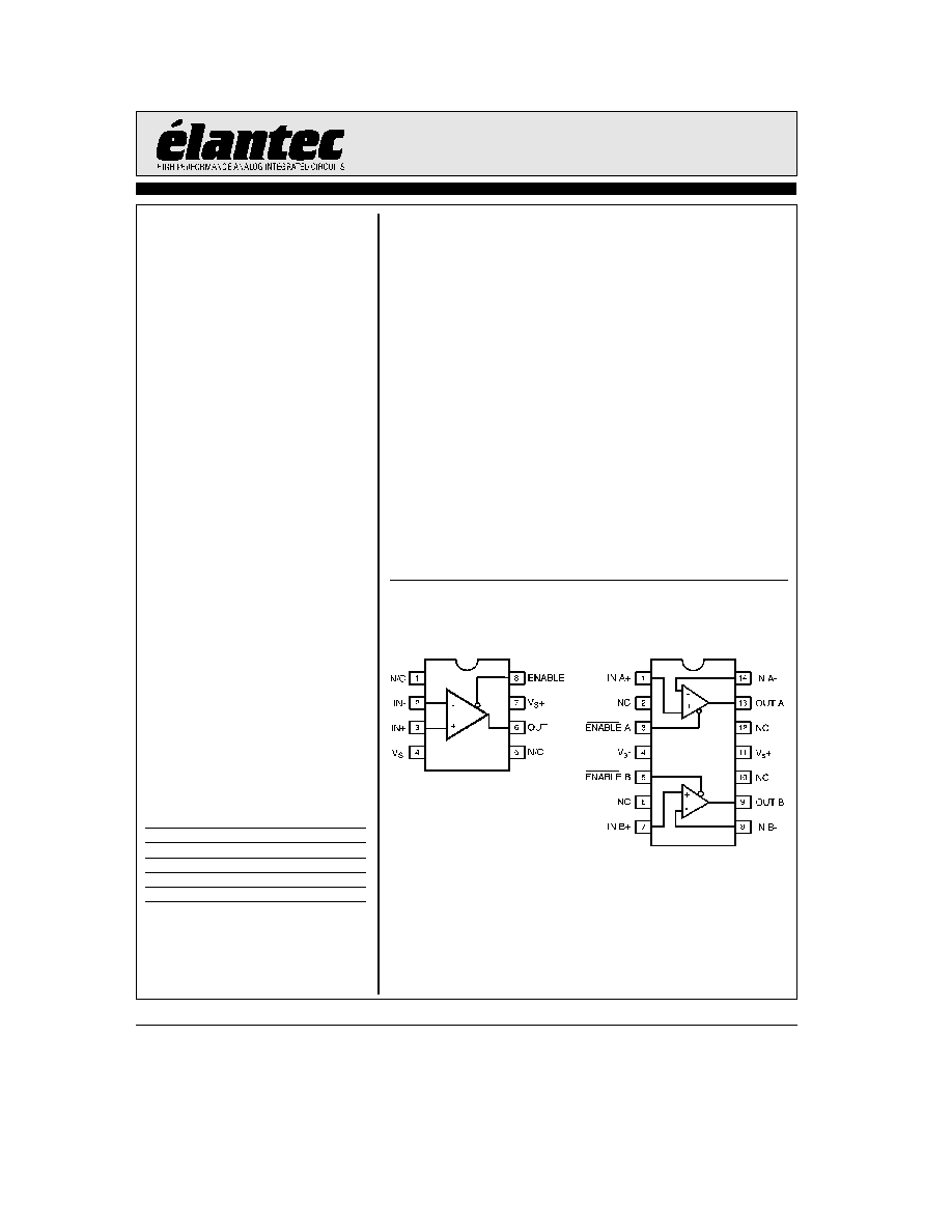
Connection Diagrams
EL2176C SO P-DIP
EL2276C SO P-DIP
2176 ≠ 1
2176 ≠ 2
Manufactured under U S Patent No 5 352 989 5 351 012 5 418 495

EL2176C EL2276C
70 MHz 1 mA Current Mode Feedback Amp w Disable
Absolute Maximum Ratings
(T
A
e
25 C)
Voltage between V
Sa
and V
Sb
a
12 6V
Common-Mode Input Voltage
V
Sb
to V
Sa
Differential Input Voltage
g
6V
Current into
a
IN or
b
IN
g
7 5 mA
Internal Power Dissipation
See Curves
Operating Ambient Temperature Range
b
40 C to
a
85 C
Operating Junction Temperature
Plastic Packages
150 C
Output Current (EL2176C)
g
120 mA
Output Current (EL2276C)
g
60 mA
Storage Temperature Range
b
65 C to
a
150 C
Important Note
All parameters having Min Max specifications are guaranteed The Test Level column indicates the specific device testing actually
performed during production and Quality inspection Elantec performs most electrical tests using modern high-speed automatic test
equipment specifically the LTX77 Series system Unless otherwise noted all tests are pulsed tests therefore T
J
e
T
C
e
T
A
Test Level
Test Procedure
I
100% production tested and QA sample tested per QA test plan QCX0002
II
100% production tested at T
A
e
25 C and QA sample tested at T
A
e
25 C
T
MAX
and T
MIN
per QA test plan QCX0002
III
QA sample tested per QA test plan QCX0002
IV
Parameter is guaranteed (but not tested) by Design and Characterization Data
V
Parameter is typical value at T
A
e
25 C for information purposes only
DC Electrical Characteristics
V
S
e
g
5V R
L
e
150
X ENABLE
e
0V T
A
e
25 C unless otherwise specified
Parameter
Description
Conditions
Min
Typ
Max
Test
Units
Level
V
OS
Input Offset Voltage
2 5
15
I
mV
TCV
OS
Average Input Offset Voltage Drift
Measured from T
MIN
to T
MAX
5
V
mV C
dV
OS
V
OS
Matching
EL2276C only
0 5
V
mV
a
I
IN
a
Input Current
0 5
5
I
mA
d
a
I
IN
a
I
IN
Matching
EL2276C only
20
V
nA
b
I
IN
b
Input Current
4
15
I
mA
d
b
I
IN
b
I
IN
Matching
EL2276C only
1 5
V
mA
CMRR
Common Mode Rejection Ratio
V
CM
e
g
3 5 V
45
50
I
dB
b
ICMR
b
Input Current Common Mode Rejection
V
CM
e
g
3 5V
4
10
I
mA V
PSRR
Power Supply Rejection Ratio
V
S
is moved from
g
4V to
g
6V
60
70
I
dB
b
IPSR
b
Input Current Power Supply Rejection
V
S
is moved from
g
4V to
g
6V
0 5
5
I
mA V
R
OL
Transimpedance
V
OUT
e
g
2 5V
150
400
I
k
X
a
R
IN
a
Input Resistance
V
CM
e
g
3 5V
1
4
I
M
X
a
C
IN
a
Input Capacitance
1 2
V
pF
CMIR
Common Mode Input Range
g
3 5
g
4 0
I
V
2
TD
is
31in

EL2176C EL2276C
70 MHz 1 mA Current Mode Feedback Amp w Disable
DC Electrical Characteristics
Contd
V
S
e
g
5V R
L
e
150
X ENABLE
e
0V T
A
e
25 C unless otherwise specified
Parameter
Description
Conditions
Min Typ Max
Test
Units
Level
V
O
Output Voltage Swing
V
S
e
g
5
g
3 5
g
4 0
I
V
V
S
e a
5 Single-Supply High
4 0
V
V
V
S
e a
5 Single-Supply Low
0 3
V
V
I
O
Output Current
EL2176C only
80
100
I
mA
EL2276C only per Amplifier
50
55
I
mA
I
S
Supply Current
ENABLE
e
2 0V per Amplifier
1
2
I
mA
I
S(DIS)
Supply Current (Disabled)
ENABLE
e
4 5V
0
20
I
mA
C
OUT(DIS)
Output Capacitance (Disabled)
ENABLE
e
4 5V
4 4
V
pF
R
EN
Enable Pin Input Resistance
Measured at ENABLE
e
2 0V 4 5V
45
85
I
k
X
I
IH
Logic ``1'' Input Current
Measured at ENABLE ENABLE
e
4 5V
b
0 04
V
mA
I
IL
Logic ``0'' Input Current
Measured at ENABLE ENABLE
e
0V
b
53
V
mA
V
DIS
Minimum Voltage at ENABLE to Disable
4 5
I
V
V
EN
Maximum Voltage at ENABLE to Enable
2 0
I
V
AC Electrical Characteristics
V
S
e
g
5V R
F
e
R
G
e
1 0 k
X R
L
e
150
X ENABLE
e
0V T
A
e
25 C unless otherwise specified
Parameter
Description
Conditions
Min
Typ
Max
Test Level
Units
b
3 dB BW
b
3 dB Bandwidth
A
V
e a
1
70
V
MHz
b
3 dB BW
b
3 dB Bandwidth
A
V
e a
2
60
V
MHz
SR
Slew Rate
V
OUT
e
g
2 5V A
V
e a
2
400
800
IV
V
ms
t
r
t
f
Rise and Fall Time
V
OUT
e
g
500 mV
4 5
V
ns
t
pd
Propagation Delay
V
OUT
e
g
500 mV
4 5
V
ns
OS
Overshoot
V
OUT
e
g
500 mV
3 0
V
%
ts
0 1% Settling
V
OUT
e
g
2 5V A
V
e b
1
40
V
ns
dG
Differential Gain
A
V
e a
2 R
L
e
150
X (Note 1)
0 15
V
%
dP
Differential Phase
A
V
e a
2 R
L
e
150
X (Note 1)
0 15
V
dG
Differential Gain
A
V
e a
1 R
L
e
500
X (Note 1)
0 02
V
%
dP
Differential Phase
A
V
e a
1 R
L
e
500
X (Note 1)
0 01
V
t
ON
Turn-On Time
A
V
e a
2 V
IN
e a
1V R
L
e
150
X (Note 2)
40
100
I
ns
t
OFF
Turn-Off Time
A
V
e a
2 V
IN
e a
1V R
L
e
150
X (Note 2)
1500
2000
I
ns
CS
Channel Separation
EL2276C only f
e
5 MHz
85
V
dB
Note 1 DC offset from 0V to 0 714V AC amplitude 286 mV
P-P
f
e
3 58 MHz
Note 2 Measured from the application of the logic signal until the output voltage is at the 50% point between initial and final
values
3
TD
is
28in
TD
is
28in
EL2176C EL2276C
70 MHz 1 mA Current Mode Feedback Amp w Disable
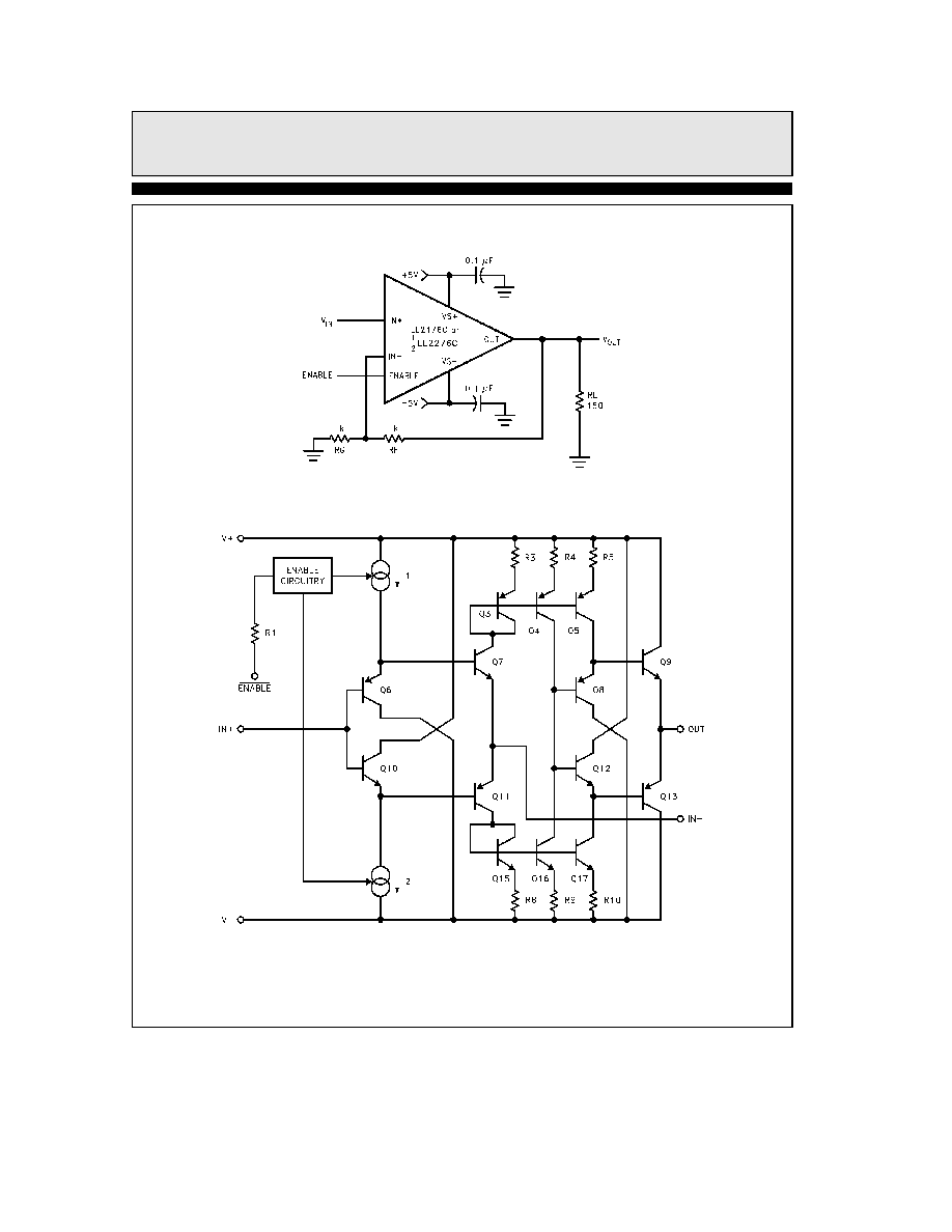
Test Circuit
(per Amplifier)
2176 ≠ 3
Simplified Schematic
(per Amplifer)
2176 ≠ 4
4
EL2176C EL2276C
70 MHz 1 mA Current Mode Feedback Amp w Disable
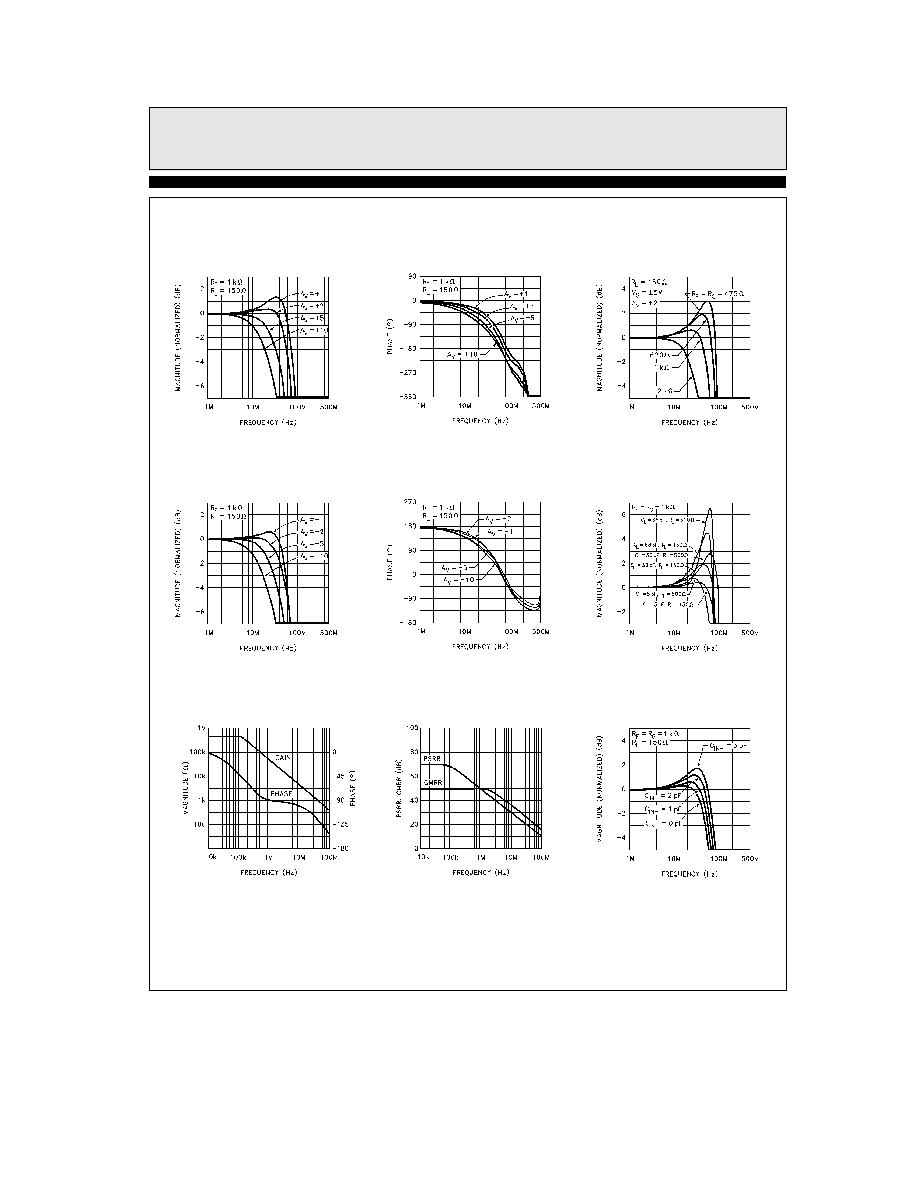
Typical Performance Curves
Frequency Response (Gain)
Non-Inverting
2176 ≠ 5
Frequency Response (Phase)
Non-Inverting
2176 ≠ 6
Various R
F
and R
G
Frequency Response for
2176 ≠ 7
Response (Gain)
Inverting Frequency
2176 ≠ 8
Response (Phase)
Inverting Frequency
2176 ≠ 9
Various R
L
and C
L
Frequency Response for
2176 ≠ 10
Transimpedance (R
OL
)
2176 ≠ 11
PSRR and CMRR
2176 ≠ 12
for Various C
INb
Frequency Response
2176 ≠ 13
5

EL2176C EL2276C
70 MHz 1 mA Current Mode Feedback Amp w Disable
Typical Performance Curves
Contd
Noise vs Frequency
Voltage and Current
2176 ≠ 14
Distortion vs Frequency
2nd and 3rd Harmonic
2176 ≠ 15
vs Frequency
Output Voltage
2176 ≠ 16
Various Non-Inverting Gains
vs Supply Voltage for
b
3 dB Bandwith and Peaking
2176 ≠ 17
Various Inverting Gains
vs Supply Voltage for
b
3 dB Bandwith and Peaking
2176 ≠ 18
vs Supply Voltage
Output Voltage Swing
2176 ≠ 19
Voltage
Supply Current vs Supply
2176 ≠ 20
vs Supply Voltage
Common-Mode Input Range
2176 ≠ 21
Supply Voltage
Slew Rate vs
2176 ≠ 22
6
EL2176C EL2276C
70 MHz 1 mA Current Mode Feedback Amp w Disable
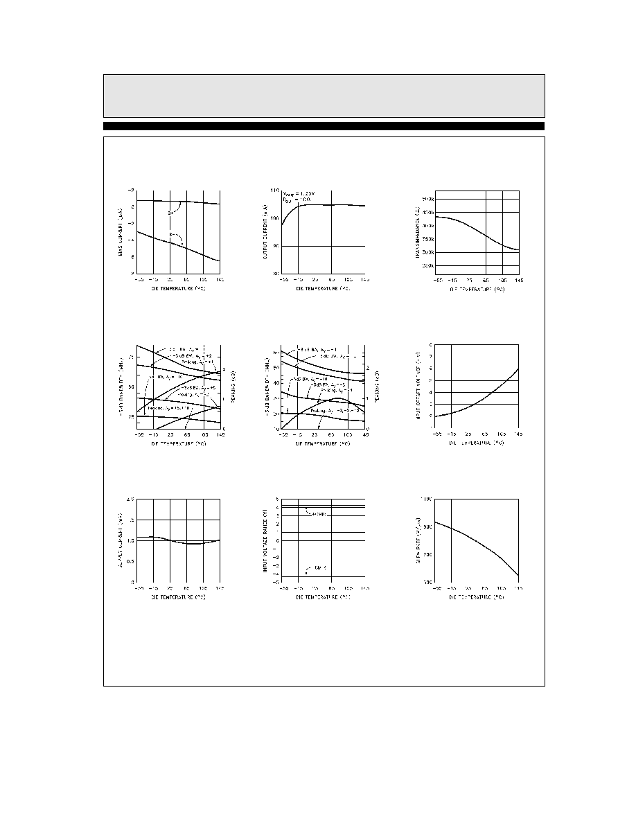
Typical Performance Curves
Contd
Die Temperature
Input Bias Current vs
2176 ≠ 23
Die Temperature
Short-Circuit Current vs
2176 ≠ 24
Die Temperature
Transimpedance (R
OL
) vs
2176 ≠ 25
Various Non-Inverting Gains
vs Die Temperature for
b
3 dB Bandwith and Peaking
2176 ≠ 26
Various Inverting Gains
vs Die Temperature for
b
3 dB Bandwith and Peaking
2176 ≠ 27
vs Die Temperature
Input Offset Voltage
2176 ≠ 28
Die Temperature
Supply Current vs
2176 ≠ 29
Die Temperature
Input Voltage Range vs
2176 ≠ 30
Die Temperature
Slew Rate vs
2176 ≠ 31
7

EL2176C EL2276C
70 MHz 1 mA Current Mode Feedback Amp w Disable
Typical Performance Curves
Contd
at 3 58 MHz A
V
e
a
2
Phase vs DC Input Voltage
Differential Gain and
2176 ≠ 32
at 3 58 MHz A
V
e
a
1
Phase vs DC Input Offset
Differential Gain and
2176 ≠ 33
Settling Accuracy
Settling Time vs
2176 ≠ 34
Small-Signal Step Response
2176 ≠ 35
Large-Signal Step Response
2176 ≠ 36
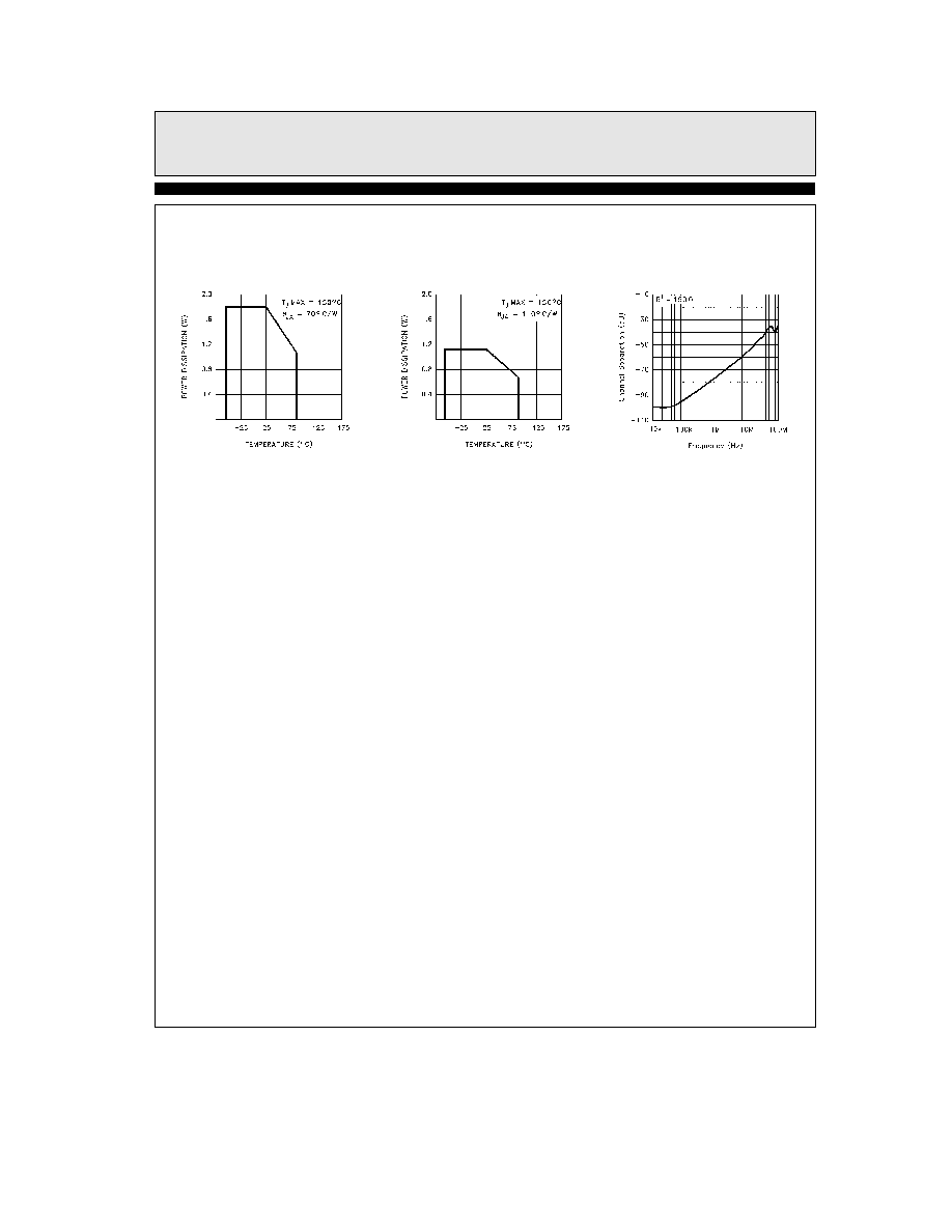
Maximum Power Dissipation
8-Pin Plastic DIP
vs Ambient Temperature
2176 ≠ 37
Maximum Power Dissipation
8-Lead SO
vs Ambient Temperature
2176 ≠ 38
8
EL2176C EL2276C
70 MHz 1 mA Current Mode Feedback Amp w Disable
Typical Performance Curves
Contd
vs Ambient Temperature
Maximum Power Dissipation
14-Pin Plastic DIP
2176 ≠ 39
vs Ambient Temperature
Maximum Power Dissipation
14-Lead SO
2176 ≠ 40
vs Frequency (EL2276)
Channel Separation
2176 ≠ 41
9
EL2176C EL2276C
70 MHz 1 mA Current Mode Feedback Amp w Disable
Applications Information
Product Description
The EL2176C EL2276C are current-feedback op-
erational amplifiers that offer a wide
b
3 dB
bandwidth of 70 MHz a low supply current of
1 mA per amplifier and the ability to disable to
0 mA Both products also feature high output
current drive The EL2176C can output 100 mA
while the EL2276C can output 55 mA per ampli-
fier The EL2176C EL2276C work with supply
voltages ranging from a single 3V to
g
6V and
they are also capable of swinging to with in 1V of
either supply on the input and the output Be-
cause of their current-feedback topology
the
EL2176C EL2276C do not have the normal gain-
bandwidth product associated with voltage-feed-
back operational amplifiers
This allows their
b
3 dB bandwidth to remain relatively constant
as closed-loop gain is increased This combina-
tion of high bandwidth and low power together
with aggressive pricing make the EL2176C
EL2276C the ideal choice for many low-power
high-bandwidth applications such as portable
computing HDSL and video processing
For Single Dual and Quad applications without
disable
consider the EL2170C (8-Pin Single)
EL2270C (8-Pin Dual) and EL2470C (14-Pin
Quad) If more AC performance is required refer
to the EL2180C EL2186C family which provides
Singles
Duals
and Quads with 250 MHz of
bandwidth while consuming 3 mA of supply cur-
rent per amplifier
Power Supply Bypassing and Printed
Circuit Board Layout
As with any high-frequency device good printed
circuit board layout is necessary for optimum
performance Ground plane construction is high-
ly recommended Lead lengths should be as short
as possible The power supply pins must be well
bypassed to reduce the risk of oscillation The
combination of a 4 7
mF tantalum capacitor in
parallel with a 0 1
mF capacitor has been shown
to work well when placed at each supply pin
For good AC performance parasitic capacitance
should be kept to a minimum especially at the
inverting input (see the Capacitance at the In-
verting Input section) Ground plane construc-
tion should be used but it should be removed
from the area near the inverting input to mini-
mize any stray capacitance at that node Carbon
or Metal-Film resistors are acceptable with the
Metal-Film resistors giving slightly less peaking
and bandwidth because of their additional series
inductance Use of sockets particularly for the
SO package should be avoided if possible Sock-
ets add parasitic inductance and capacitance
which will result in some additional peaking and
overshoot
Disable Power-Down
The EL2176C EL2276C amplifiers can be dis-
abled placing their output in a high-impedance
state When disabled each amplifier's supply cur-
rent is reduced to 0 mA
Each EL2176C
EL2276C
amplifier
is
disabled
when
its
ENABLE pin is floating or pulled up to within
0 5V of the positive supply Similarly each am-
plifier is enabled by pulling its ENABLE pin at
least 3V below the positive supply For
g
5V sup-
plies this means that an EL2176C EL2276C am-
plifier will be enabled when ENABLE is at 2V or
less and disabled when ENABLE is above 4 5V
Although the logic levels are not standard TTL
this choice of logic voltages allows the EL2176C
EL2276C to be enabled by tying ENABLE to
ground even in
a
3V single-supply applications
The ENABLE pin can be driven from CMOS
outputs or open-collector TTL
When enabled supply current does vary some-
what with the voltage applied at ENABLE For
example
with
the
supply
voltages
of
the
EL2176C at
g
5V if ENABLE is tied to
b
5V
(rather than ground) the supply current will in-
crease about 15% to 1 15 mA
Capacitance at the Inverting Input
Any manufacturer's high-speed voltage- or cur-
rent-feedback amplifier can be affected by stray
capacitance at the inverting input For inverting
gains this parasitic capacitance has little effect
because the inverting input is a virtual ground
but for non-inverting gains this capacitance (in
conjunction with the feedback and gain resistors)
creates a pole in the feedback path of the amplifi-
er This pole if low enough in frequency has the
same destabilizing effect as a zero in the forward
open-loop response The use of large value feed-
10

EL2176C EL2276C
70 MHz 1 mA Current Mode Feedback Amp w Disable
Applications Information
Contd
back and gain resistors further exacerbates the
problem by further lowering the pole frequency
The EL2176C EL2276C have been specially de-
signed to reduce power dissipation in the feed-
back network by using large 1 0 k
X feedback and
gain resistors With the high bandwidths of these
amplifiers these large resistor values would nor-
mally cause stability problems when combined
with parasitic capacitance but by internally can-
celing the effects of a nominal amount of parasit-
ic capacitance
the EL2176C EL2276C remain
very stable For less experienced users this fea-
ture makes the EL2176C EL2276C much more
forgiving and therefore easier to use than other
products not incorporating this proprietary cir-
cuitry
The experienced user with a large amount of PC
board layout experience may find in rare cases
that the EL2176C EL2276 C have less band-
width than expected In this case the inverting
input may have less parasitic capacitance than
expected by the internal compensation circuitry
of the EL2176C EL2276C The reduction of feed-
back resistor values (or the addition of a very
small amount of external capacitance at the in-
verting input e g
0 5 pF) will increase band-
width as desired Please see the curves for Fre-
quency Response for Various R
F
and R
G
and
Frequency Response for Various C
IN
b
Feedback Resistor Values
The EL2176C EL2276C have been designed and
specified at gains of
a
1 and
a
2 with R
F
e
1 0 k
X This value of feedback resistor gives
70 MHz of
b
3 dB bandwidth at A
V
e
a
1 with
about 1 5 dB of peaking and 60 MHz of
b
3 dB
bandwidth at A
V
e
a
2 with about 0 5 dB of
peaking Since the EL2176C EL2276C are cur-
rent-feedback amplifiers it is also possible to
change the value of R
F
to get more bandwidth
As seen in the curve of Frequency Response For
Various R
F
and R
G
bandwidth and peaking can
be easily modified by varying the value of the
feedback resistor
Because the EL2176C is a current-feedback am-
plifier the gain-bandwidth product is not a con-
stant for different closed-loop gains This feature
actually allows the EL2176C EL2276C to main-
tain about the same
b
3 dB bandwidth regard-
less of closed-loop gain However as closed-loop
gain is increased bandwidth decreases slightly
while stability increases
Since the loop stability is improving with higher
closed-loop gains it becomes possible to reduce
the value of R
F
below the specified 1 0 k
X and
still retain stability resulting in only a slight loss
of bandwidth with increased closed-loop gain
Supply Voltage Range and Single-
Supply Operation
The EL2176C EL2276C have been designed to
operate with supply voltages having a span of
greater than 3V and less than 12V In practical
terms this means that the EL2176C EL2276C
will operate on dual supplies ranging from
g
1 5V
to
g
6V With a single-supply the EL2176C will
operate from
a
3V to
a
12V
As supply voltages continue to decrease it be-
comes necessary to provide input and output
voltage ranges that can get as close as possible to
the supply voltages
The EL2176C EL2276C
have an input voltage range that extends to with-
in 1V of either supply So for example on a sin-
gle
a
5V supply the EL2176C EL2276C have an
input range which spans from 1V to 4V The out-
put range of the EL2176C EL2276C is also quite
large extending to within 1V of the supply rail
On a
g
5V supply the output is therefore capable
of swinging from
b
4V to
a
4V Single-supply
output range is even larger because of the in-
creased negative swing due to the external pull-
down resistor to ground On a single
a
5V sup-
ply output voltage range is about 0 3V to 4V
Video Performance
For good video performance an amplifier is re-
quired to maintain the same output impedance
and the same frequency response as DC levels are
changed at the output This is especially difficult
when driving a standard video load of 150
X be-
cause of the change in output current with DC
level Until the EL2176C EL2276C good Differ-
ential Gain could only be achieved by running
high idle currents through the output transistors
(to reduce variations in output impedance)
These currents were typically in excess of the
11

EL2176C EL2276C
70 MHz 1 mA Current Mode Feedback Amp w Disable
Applications Information
Contd
entire 1 mA supply current of each EL2176C
EL2276C amplifier Special circuitry has been in-
corporated in the EL2176C EL2276C to reduce
the variation of output impedance with current
output This results in dG and dP specifications
of 0 15% and 0 15 while driving 150
X at a gain
of
a
2
Video Performance has also been measured with
a 500
X load at a gain of
a
1 Under these condi-
tions the EL2176C EL2276C have dG and dP
specifications of 0 01% and 0 02
respectively
while driving 500
X at A
V
e
a
1
Output Drive Capability
In spite of its low 1 mA of supply current the
EL2176C is capable of providing a minimum of
g
80 mA of output current Similarly each am-
plifier of the EL2276C is capable of providing a
minimum of
g
50 mA These output drive levels
are unprecedented in amplifiers running at these
supply currents With a minimum
g
80 mA of
output drive the EL2176C is capable of driving
50
X loads to
g
4V making it an excellent choice
for driving isolation transformers in telecommu-
nications applications Similarly the
g
50 mA
minimum output drive of each EL2276C amplifi-
er allows swings of
g
2 5V into 50
X loads
Driving Cables and Capacitive Loads
When used as a cable driver double termination
is always recommended for reflection-free per-
formance For those applications the back-termi-
nation series resistor will decouple the EL2176C
EL2276C from the cable and allow extensive ca-
pacitive drive However other applications may
have high capacitive loads without a back-termi-
nation resistor In these applications a small se-
ries resistor (usually between 5
X and 50X) can be
placed in series with the output to eliminate most
peaking The gain resistor (R
G
) can then be cho-
sen to make up for any gain loss which may be
created by this additional resistor at the output
In many cases it is also possible to simply in-
crease the value of the feedback resistor (R
F
) to
reduce the peaking
Current Limiting
The EL2176C EL2276C have no internal cur-
rent-limiting circuitry If any output is shorted
it is possible to exceed the Absolute Maximum
Ratings for output current or power dissipation
potentially resulting in the destruction of the de-
vice
Power Dissipation
With the high output drive capability of the
EL2176C EL2276C it is possible to exceed the
150 C Absolute Maximum junction temperature
under certain very high load current conditions
Generally speaking when R
L
falls below about
25
X it is important to calculate the maximum
junction temperatu re (T
Jmax
) for the application
to determine if power-supply voltages load con-
ditions or package type need to be modified for
the EL2176C EL2276C to remain in the safe op-
erating area These parameters are calculated as
follows
T
JMAX
e
T
MAX
a
(
i
JA
n
PD
MAX
)
1
where
T
MAX
e
Maximum Ambient Temperature
i
JA
e
Thermal Resistance of the Package
n
e
Number of Amplifiers in the Pack-
age
PD
MAX
e
Maximum Power Dissipation of
Each Amplifier in the Package
PD
MAX
for each amplifier can be calculated as
follows
PD
MAX
e
(2
V
S
I
SMAX
)
a
(V
S
b
V
OUTMAX
)
(V
OUTMAX
R
L
))
2
where
V
S
e
Supply Voltage
I
SMAX
e
Maximum Supply Current of 1
Amplifier
V
OUTMAX
e
Max Output Voltage of the Ap-
plication
R
L
e
Load Resistance
12
EL2176C EL2276C
70 MHz 1 mA Current Mode Feedback Amp w Disable
Typical Application Circuits
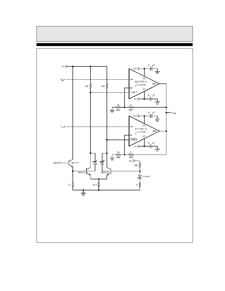
Low Power Multiplexer with Single-Ended TTL Input
2176 ≠ 42
13
EL2176C EL2276C
70 MHz 1 mA Current Mode Feedback Amp w Disable
Typical Application Circuits
Contd
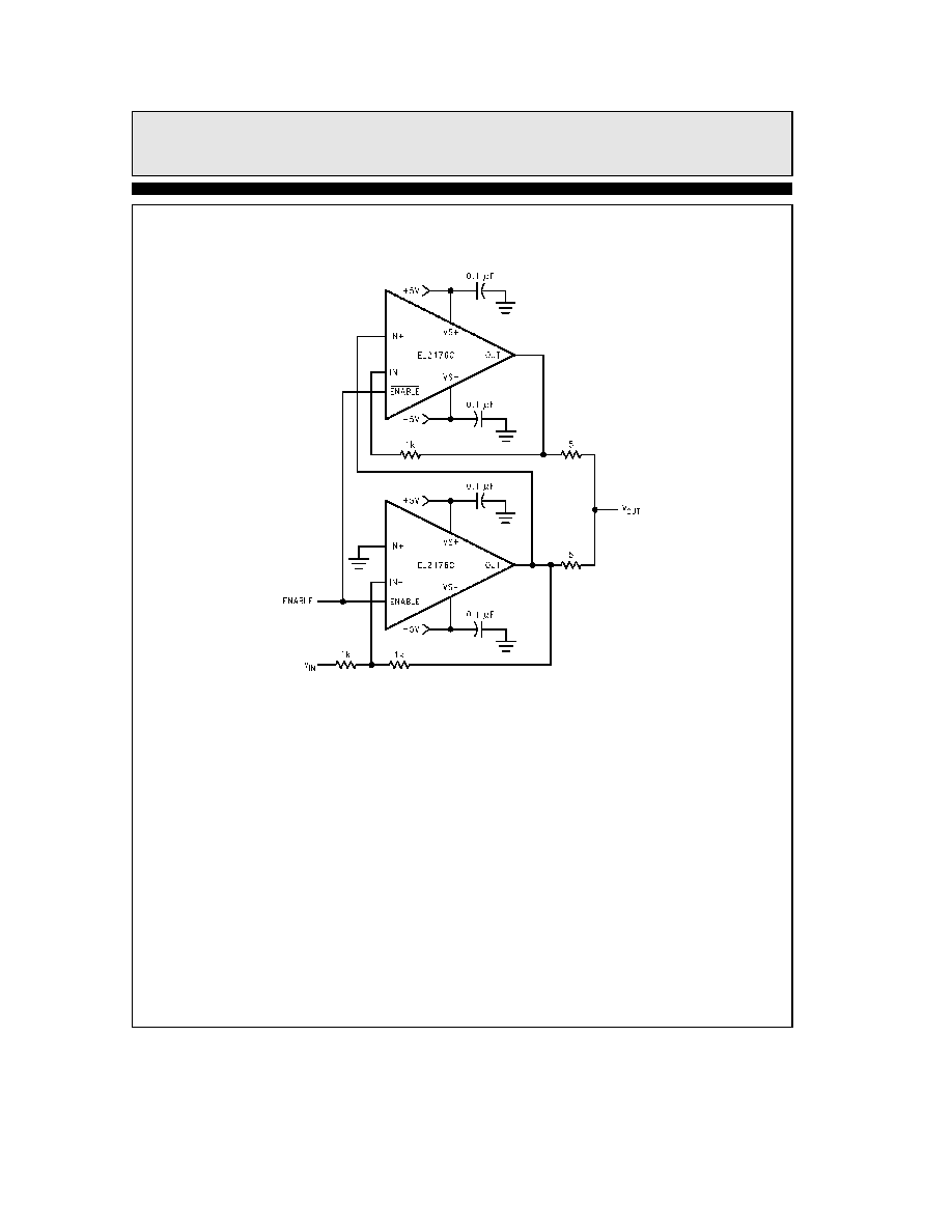
Inverting 200 mA Output Current Distribution Amplifier
2176 ≠ 43
14
EL2176C EL2276C
70 MHz 1 mA Current Mode Feedback Amp w Disable
Typical Application Circuits
Contd
Differential Line-Driver Receiver
2176 ≠ 44
15
EL2176C EL2276C
70 MHz 1 mA Current Mode Feedback Amp w Disable
Typical Application Circuits
Contd
Fast-Settling Precision Amplifier
2176 ≠ 45
16

EL2176C EL2276C
70 MHz 1 mA Current Mode Feedback Amp w Disable
EL2176C EL2276C Macromodel
Revision A March 1995
Transimpedance Stage
AC characteristics used Rf
e
Rg
e
1K
X RL
e
150
X
Connections
a
input
g1 0 18 17 0 1 0
l
b
input
rol 18 0 400K
l
l
a
Vsupply
cdp 18 0 1 9pF
l
l
l
b
Vsupply
l
l
l
l
output
Output Stage
l
l
l
l
l
subckt EL2176 el
3
2
7
4
6
q1 4 18 19 qp
q2 7 18 20 qn
Input Stage
q3 7 19 21 qn
q4 4 20 22 qp
e1 10 0 3 0 1 0
r7 21 6 4
vis 10 9 0V
r8 22 6 4
h2 9 12 vxx 1 0
ios1 7 19 0 4mA
r1 2 11 165
ios2 20 4 0 4mA
l1 11 12 25nH
iinp 3 0 0 5uA
Supply Current
iinm 2 0 4uA
r12 3 0 4Meg
ips 7 4 1nA
Slew Rate Limiting
Error Terms
h1 13 0 vis 600
ivos 0 23 2mA
r2 13 14 1K
vxx 23 0 0V
d1 14 0 dclamp
e4 24 0 3 0 1 0
d2 0 14 dclamp
e5 25 0 7 0 1 0
e6 26 0 4 0
b
1 0
High Frequency Pole
r9 24 23 0 316K
r10 25 23 3 2K
e2 30 0 14 0 0 00166666666
r11 26 23 3 2K
l3 30 17 0 5uH
c5 17 0 0 69pF
Models
r5 17 0 300
model qn npn(is
e
5e-15 bf
e
200 tf
e
0 01nS)
model qp pnp(is
e
5e-15 bf
e
200 tf
e
0 01nS)
model dclamp d(is
e
1e-30 ibv
e
0 266
a
bv
e
1 3v n
e
4)
ends
17
TD
is
52in

EL2176C EL2276C
70 MHz 1 mA Current Mode Feedback Amp w Disable
EL2176C EL2276C Macromodel
Contd
2176 ≠ 46
18

BLANK
19

EL2176CEL2276C
December
1995
Rev
B
EL2176C EL2276C
70 MHz 1 mA Current Mode Feedback Amp w Disable
General Disclaimer
Specifications contained in this data sheet are in effect as of the publication date shown Elantec Inc reserves the right to make changes
in the circuitry or specifications contained herein at any time without notice Elantec Inc assumes no responsibility for the use of any
circuits described herein and makes no representations that they are free from patent infringement
Elantec Inc
1996 Tarob Court
Milpitas CA 95035
Telephone (408) 945-1323
(800) 333-6314
Fax (408) 945-9305
European Office 44-71-482-4596
WARNING
Life Support Policy
Elantec Inc products are not authorized for and should not be
used within Life Support Systems without the specific written
consent of Elantec Inc Life Support systems are equipment in-
tended to support or sustain life and whose failure to perform
when properly used in accordance with instructions provided can
be reasonably expected to result in significant personal injury or
death Users contemplating application of Elantec Inc products
in Life Support Systems are requested to contact Elantec Inc
factory headquarters to establish suitable terms
conditions for
these applications Elantec Inc 's warranty is limited to replace-
ment of defective components and does not cover injury to per-
sons or property or other consequential damages
Printed in U S A
20