 | –≠–ª–µ–∫—Ç—Ä–æ–Ω–Ω—ã–π –∫–æ–º–ø–æ–Ω–µ–Ω—Ç: EL2311C | –°–∫–∞—á–∞—Ç—å:  PDF PDF  ZIP ZIP |
Note: All information contained in this data sheet has been carefully checked and is believed to be accurate as of the date of publication; however, this data sheet cannot be a "controlled document". Current revisions, if any, to these
specifications are maintained at the factory and are available upon your request. We recommend checking the revision level before finalization of your design documentation.
© 2001 Elantec Semiconductor, Inc.
E
L
2
2
1
0
C
/
1
1
C
,
E
L
2
3
1
0
C
/
1
1
C
,
E
L
2
4
1
0
C
/
1
1
C
General Description
This family of dual, triple, and quad operational amplifiers built using
Elantec's Complementary Bipolar process offers unprecedented high
frequency performance at a very low cost. They are suitable for any
application such as consumer video, where traditional DC perfor-
mance specifications are of secondary importance to the high
frequency specifications. On ±5V supplies at a gain of +1 the
EL2210C, EL2310C, and EL2410C will drive a 150
load to +2V,
---
-1V with a bandwidth of 50MHz and a channel-to-channel isolation of
60dB or more. At a gain of +2, the EL2211C, EL2311C, and EL2411C
will drive a 150
load to +2V, -1V with a bandwidth of 100MHz with
the same channel-to-channel isolation. All four achieve 0.1dB band-
width at 5MHz.
The power supply operating range is fixed at ±5V or +10/0V. In single
supply operation the inputs and outputs will operate to ground. Each
amplifier draws only 7mA of supply current.
Connection Diagrams
1
2
3
4
14
13
12
11
5
6
7
10
9
8
1
2
3
4
14
13
12
11
5
6
7
10
9
8
EL2210C/EL2211C
EL2210C/EL2211C
-
+
NC
NC
NC
VS+
OUT2
IN2-
IN2+
VS-
IN1+
IN1-
OUT1
IN3+
IN3-
OUT3
OUT1
IN1-
IN1+
V+
OUT4
IN4-
IN4+
V-
IN2+
IN2-
OUT2
IN3+
IN3-
OUT3
-
+
- +
-
+
- +
-
+
- +
1
2
3
4
8
7
6
5
EL2210C/EL2211C
- +
-
+
OUT
IN1-
IN1+
V-
V+
OUT2
IN2-
IN2+
Features
∑ Stable at gain of 2 and 100MHz
gain_bandwidth product
(EL2211C, EL2311C, &
EL2411C)
∑ Stable at gain of 1 and 50MHz
gain_bandwidth product
(EL2210C, EL2310C, &
EL2410C)
∑ 130V/µs slew rate
∑ Drives 150
load to video levels
∑ Inputs and outputs operate at
negative supply rail
∑ ±5V or +10V supplies
∑ -60dB isolation at 4.2MHz
Applications
∑ Consumer video amplifiers
∑ Active filters/integrators
∑ Cost-sensitive applications
∑ Single supply amplifiers
Ordering Information
Part No
Package
Tape & Reel
Outline #
EL2210CN
8-Pin PDIP
-
MDP0031
EL2210CS
8-Pin SO
-
MDP0027
EL2210CS-T7
8-Pin SO
7"
MDP0027
EL2210CS-T13
8-Pin SO
13"
MDP0027
EL2211CN
8-Pin PDIP
-
MDP0031
EL2211CS
8-Pin SO
-
MDP0027
EL2310CN
8-Pin PDIP
-
MDP0031
EL2310CS
8-Pin SO
-
MDP0027
EL2311CN
8-Pin PDIP
-
MDP0031
EL2311CS
8-Pin SO
-
MDP0027
EL2410CN
14-Pin PDIP
-
MDP0031
EL2410CS
14-Pin SO
-
MDP0027
EL2410CS-T7
14-Pin SO
7"
MDP0027
EL2410CS-T13
14-Pin SO
13"
MDP0027
EL2411CN
14-Pin PDIP
-
MDP0031
EL2411CS
14-Pin SO
-
MDP0027
EL2210C/11C, EL2310C/11C, EL2410C/11C
Low Cost, Dual, Triple and Quad Video Op Amps
A
u
g
u
s
t
6
,
2
0
0
1
2
EL2210C/11C, EL2310C/11C, EL2410C/11C
Low Cost, Dual, Triple and Quad Video Op Amps
E
L
2
2
1
0
C
/
1
1
C
,
E
L
2
3
1
0
C
/
1
1
C
,
E
L
2
4
1
0
C
/
1
1
C
Absolute Maximum Ratings
(T
A
= 25∞C)
Total Voltage Supply
18V
Input Voltage
±V
S
Differential Input Voltage
6V
Peak Output Current
75mA (per amplifier)
Power Dissipation
See Curves
Storage Temperature Range
-65∞C to +150∞C
Operating Temperature Range
-40∞C to +85∞C
Die Junction Temperature
+150∞C
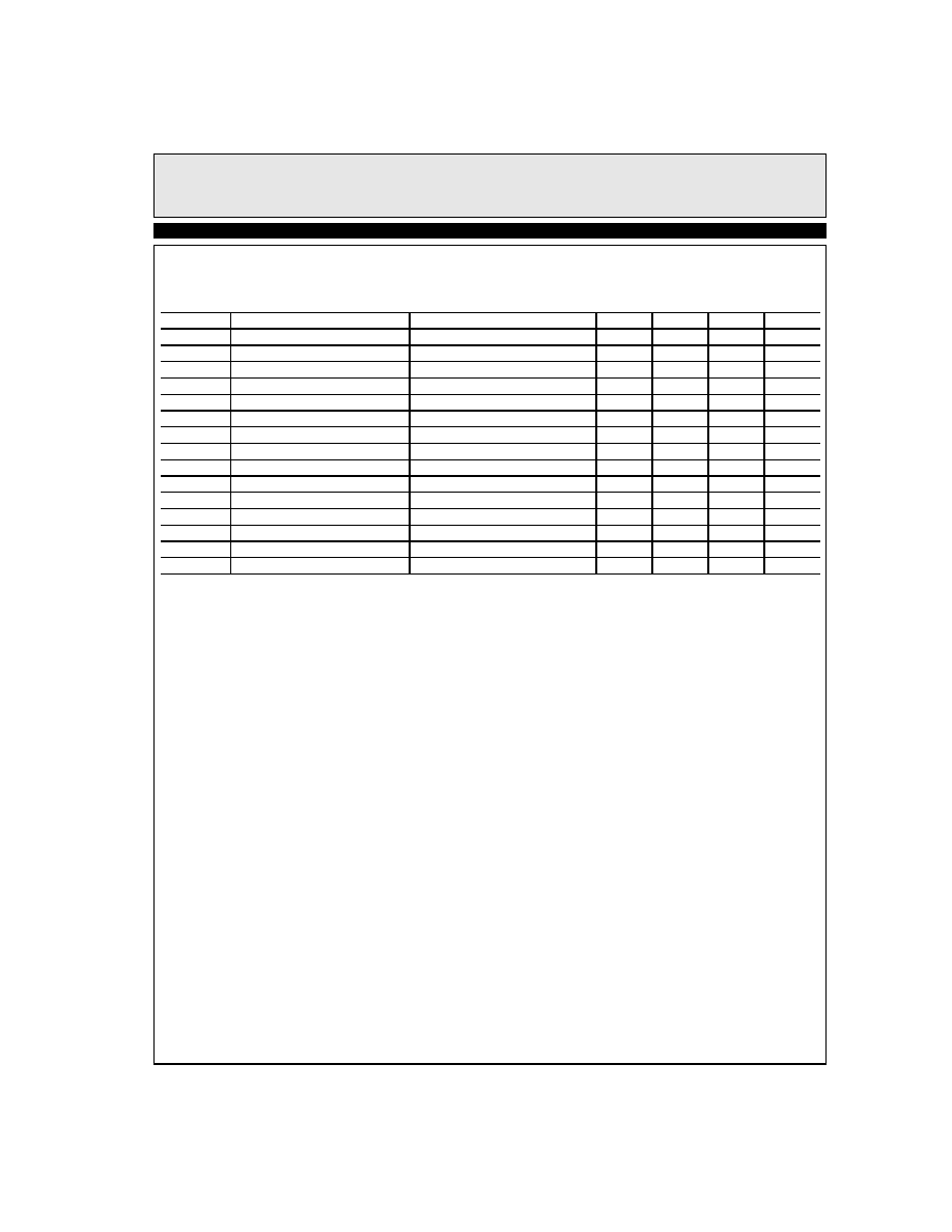
EL2210C, EL2310C, EL2410C - DC Electrical Characteristics
V
S
= ±5V, R
L
= 1k
, T
A
= 25∞C unless otherwise noted.
Parameter
Description
Conditions
Min
Typ
Max
Unit
V
OS
Input Offset Voltage
10
20
mV
EL2310C only
10
25
mV
EL2311C only
5
25
mV
TCV
OS
Average Offset Voltage Drift
[1]
1. A heat-sink is required to keep junction temperature below absolute maximum when an output is shorted
-25
µV/∞C
I
B
Input Bias Current
-15
-7
-3
µA
I
OS
Input Offset Current
0.5
1.5
µA
TCI
OS
Average Offset Current Drift
[1]
-7
nA/∞C
A
VOL
Open-Loop Gain
V
OUT
= ±2V, R
L
= 1k
160
250
V/V
V
OUT
= +2V/0V, R
L
= 150
160
250
PSRR
Power Supply Rejection
V
S
= ±4.5V to ±5.5V
50
60
dB
CMRR
Common Mode Rejection
V
CM
= ±2.4V, V
OUT
= 0V
60
80
dB
CMIR
Common Mode Input Range
V
S
= ±5V
-5/+3
V
V
OUT
Output Voltage Swing
R
L
= R
F
= 1k
R
L
to GND
-2.5
-3, 3
2.7
V
R
L
= R
F
= 1k
+150æ to GND
-0.45
-0.6, 2.9
2.5
R
L
= R
F
= 1k
R
L
to V
EE
-4.95
3
I
SC
Output Short Circuit Current
Output to GND (Note 1)
75
125
mA
I
S
Supply Current
No Load (per channel)
5.5
6.8
10
mA
R
IN
Input Resistance
Differential
150
k
Common Mode
1.5
M
C
IN
Input Capacitance
A
V
= +1 @ 10MHz
1
pF
R
OUT
Output Resistance
0.150
PSOR
Power Supply Operating Range
Dual Supply
±4.5
±6.5
V
Single Supply
9
13
Important Note:
All parameters having Min/Max specifications are guaranteed. Typ values are for information purposes only. Unless otherwise noted, all tests are at the
specified temperature and are pulsed tests, therefore: T
J
= T
C
= T
A
.
3
EL2210C/11C, EL2310C/11C, EL2410C/11C
Low Cost, Dual, Triple and Quad Video Op Amps
E
L
2
2
1
0
C
/
1
1
C
,
E
L
2
3
1
0
C
/
1
1
C
,
E
L
2
4
1
0
C
/
1
1
C
EL2211C, EL2311C, EL2411C - DC Electrical Characteristics
V
S
= ±5V, R
L
= 1k
, A
V
= +2, T
A
= 25∞C unless otherwise noted.
Parameter
Description
Conditions
Min
Typ
Max
Unit
V
OS
Input Offset Voltage
5
12
mV
TCV
OS
Average Offset Voltage Drift
[1]
-25
µV/∞C
I
B
Input Bias Current
-15
-7
-3
µA
I
OS
Input Offset Current
0.5
1.5
µA
TCI
OS
Average Offset Current Drift
[1]
-7
nA/∞C
A
VOL
Open-Loop Gain
V
OUT
= ±2V, R
L
= 1k
250
380
V/V
V
OUT
= +2V/0V, R
L
= 150
250
380
PSRR
Power Supply Rejection
V
S
= ±4.5V to ±5.5V
55
68
dB
CMRR
Common Mode Rejection
V
CM
= ±2.5V, V
OUT
= 0V
70
90
dB
CMIR
Common Mode Input Range
V
S
= ±5V
-5/+3
V
V
OUT
Output Voltage Swing
R
L
= R
F
= 1k
R
L
to GND
2.5
-3.5, 3.3
2.7
V
R
L
= R
F
= 1k
+150æ to GND
-0.45
-0.6, 2.9
2.5
R
L
= R
F
= 1k
R
L
to V
EE
-4.95
3
I
SC
Output Short Circuit Current
Output to GND (Note 1)
75
125
mA
I
S
Supply Current
No Load
5.5
6.8
10
mA
R
IN
Input Resistance
Differential
150
k
Common Mode
1.5
M
C
IN
Input Capacitance
A
V
= +1 @ 10MHz
1
pF
R
OUT
Output Resistance
0.150
PSOR
Power Supply Operating Range
Dual Supply
±4.5
±6.5
V
Single Supply
9
13
1. A heat-sink is required to keep junction temperature below absolute maximum when an output is shorted
4
EL2210C/11C, EL2310C/11C, EL2410C/11C
Low Cost, Dual, Triple and Quad Video Op Amps
E
L
2
2
1
0
C
/
1
1
C
,
E
L
2
3
1
0
C
/
1
1
C
,
E
L
2
4
1
0
C
/
1
1
C
EL2210C, EL2310C, EL2410C - Closed-Loop AC Characteristics
V
S
= ±5V, AC Test Figure 1, T
A
= 25∞C unless otherwise noted.
Parameter
Description
Conditions
Min
Typ
Max
Unit
BW
-3dB Bandwidth (V
OUT
= 0.4V
PP
)
A
V
= +1
110
MHz
BW
±0.1 dB Bandwidth (V
OUT
= 0.4V
PP
)
A
V
= +1
12
MHz
GBWP
Gain Bandwidth Product
55
MHz
PM
Phase Margin
60
∞C
SR
Slew Rate
85
130
V/µs
FBWP
Full Power Bandwidth
[1]
8
11
MHz
t
r
, t
f
Rise Time, Fall Time
0.1V Step
2
ns
OS
Overshoot
0.1V Step
15
%
t
PD
Propagation Delay
3.5
ns
t
S
Settling to 0.1% (A
V
= 1)
V
S
= ±5V, 2V Step
80
ns
d
G
Differential Gain
[2]
NTSC/PAL
0.1
%
d
P
Differential Phase
[2]
NTSC/PAL
0.2
∞C
e
N
Input Noise Voltage
10kHz
15
nV/
Hz
i
N
Input Noise Current
10kHz
1.5
pA/
Hz
CS
Channel Separation
P = 5MHz
55
dB
1. For V
S
= ±5V, V
OUT
= 4 V
PP
. Full power bandwidth is based on slew rate measurement using: FPBW = SR/(2pi * V
peak
)
2. Video performance measured at V
S
= ±5V, A
V
= +2 with 2 times normal video level across R
L
= 150
5
EL2210C/11C, EL2310C/11C, EL2410C/11C
Low Cost, Dual, Triple and Quad Video Op Amps
E
L
2
2
1
0
C
/
1
1
C
,
E
L
2
3
1
0
C
/
1
1
C
,
E
L
2
4
1
0
C
/
1
1
C
EL2211C, EL2311C, EL2411C - Closed-Loop AC Characteristics
V
S
= ±5V, AC Test Figure 1, T
A
= 25∞C unless otherwise noted.
Parameter
Description
Conditions
Min
Typ
Max
Unit
BW
-3dB Bandwidth (V
OUT
= 0.4 V
PP
)
A
V
= +2
100
MHz
BW
±0.1dB Bandwidth (V
OUT
= 0.4 V
PP
)
A
V
= +2
8
MHz
GBWP
Gain Bandwidth Product
130
MHz
PM
Phase Margin
60
∞C
SR
Slew Rate
100
140
V/µs
FBWP
Full Power Bandwidth
[1]
8
11
MHz
t
r
, t
f
Rise Time, Fall Time
0.1V Step
2.5
ns
OS
Overshoot
0.1V Step
6
%
t
PD
Propagation Delay
3.5
ns
t
S
Settling to 0.1% (A
V
= 1)
V
S
= ±5V, 2V Step
80
ns
d
G
Differential Gain
[2]
NTSC/PAL
0.04
%
d
P
Differential Phase
[2]
NTSC/PAL
0.15
∞C
e
N
Input Noise Voltage
10kHz
15
nV/
Hz
i
N
Input Noise Current
10kHz
1.5
pA/
Hz
CS
Channel Separation
P = 5MHz
55
dB
1. For V
S
= ±5V, V
OUT
= 4 V
PP
. Full power bandwidth is based on slew rate measurement using: FPBW = SR/(2pi * V
peak
)
2. Video performance measured at V
S
= ±5V, A
V
= +2 with 2 times normal video level across R
L
= 150
.

6
EL2210C/11C, EL2310C/11C, EL2410C/11C
Low Cost, Dual, Triple and Quad Video Op Amps
E
L
2
2
1
0
C
/
1
1
C
,
E
L
2
3
1
0
C
/
1
1
C
,
E
L
2
4
1
0
C
/
1
1
C
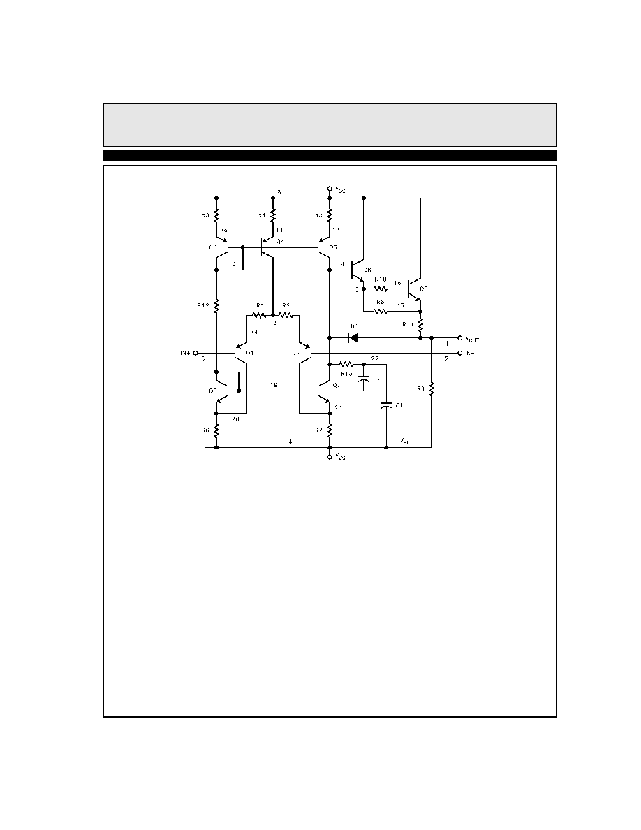
Simplified Block Diagram
Typical Performance Curves
Package Power Dissipation vs Ambient Temp.
JEDEC JESD51-3 Low Effective Thermal Conductivity Test Board
1.2
1
0.8
0.6
0.4
0.2
0
0
25
50
75
100
125
150
85
Package Power Dissipation vs Ambient Temp.
JEDEC JESD51-3 Low Effective Thermal Conductivity Test Board
1.8
1.6
1.4
1.2
0.8
0.4
0
0
25
50
75
100
125
150
85
1
0.6
0.2
Ambient Temperature (∞C)
P
o
w
e
r
D
i
s
s
i
p
a
t
i
o
n
(
W
)
Ambient Temperature (∞C)
P
o
w
e
r
D
i
s
s
i
p
a
t
i
o
n
(
W
)
1.042W
781W
JA
=120∞C/W
SO8
SO14
JA
=160∞C/W
1.54W
1.25W
JA
=81∞C/W
PDIP8
PDIP14
JA
=100∞C/W

7
EL2210C/11C, EL2310C/11C, EL2410C/11C
Low Cost, Dual, Triple and Quad Video Op Amps
E
L
2
2
1
0
C
/
1
1
C
,
E
L
2
3
1
0
C
/
1
1
C
,
E
L
2
4
1
0
C
/
1
1
C
Application Information
Product Description
The EL2210C, EL2310C, and EL2410C are dual, triple,
and quad operational amplifiers stable at a gain of 1. The
EL2211C, EL2311C, and EL2411C are dual, triple, and
quad operational amplifiers stable at a gain of 2. All six
are built on Elantec's proprietary complimentary process
and share the same voltage mode feedback topology.
This topology allows them to be used in a variety of
applications where current mode feedback amplifiers are
not appropriate because of restrictions placed on the
feedback elements. These products are especially
designed for applications where high bandwidth and
good video performance characteristics are desired but
the higher cost of more flexible and sophisticated prod-
ucts are prohibitive.
Power Supplies
These amplifiers are designed to work at a supply volt-
age difference of 10V to 12V. These amplifiers will
work on any combination of ± supplies. All electrical
characteristics are measured with ±5V supplies. Below
9V total supply voltage the amplifiers' performance will
degrade dramatically. The quiescent current is a direct
function of total supply voltage. With a total supply volt-
age of 12V the quiescent supply current will increase
from a typical 6.8mA per amplifier to 10mA per
amplifier.
Output Swing vs Load
Please refer to the simplified block diagram. These
amplifiers provide an NPN pull-up transistor output and
a passive 1250
pull-down resistor to the most negative
supply. In an application where the load is connected to
V
S
- the output voltage can swing to within 200mV of
V
S
-. In split supply applications where the DC load is
connected to ground the negative swing is limited by the
voltage divider formed by the load, the internal 1250
resistor and any external pull-down resistor. If R
L
were
150
then it and the 1250
internal resistor limit the
maximum negative swing to
Or
-
-0.53V
The negative swing can be increased by adding an exter-
nal resistor of appropriate value from the output to the
negative supply. The simplified block diagram shows an
820
external pull-down resistor. This resistor is in par-
allel with the internal 1250
resistor. This will increase
the negative swing to
Or -1.16V
Power Dissipation and Loading
Without any load and a 10V supply difference the power
dissipation is 70mW per amplifier. At 12V supply dif-
ference this increases to 105mW per amplifier. At 12V
this translates to a junction temperature rise above ambi-
ent of 33∞C for the dual and 40∞C for the quad amplifier.
When the amplifiers provide load current the power dis-
sipation can rapidly rise.
In ±5V operation each output can drive a grounded
150
load to more than 2V. This operating condition
will not exceed the maximum junction temperature limit
as long as the ambient temperature is below 85∞C, the
device is soldered in place, and the extra pull-down
resistor is 820
or more.
If the load is connected to the most negative voltage
(ground in single supply operation) you can easily
exceed the absolute maximum die temperature. For
example the maximum die temperature should be
150∞C. At a maximum expected ambient temperature of
85∞C, the total allowable power dissipation for the SO8
package would be:
At 12V total supply voltage each amplifier draws a max-
imum of 10mA and dissipates 12V * 10mA = 120mW or
240mW for the dual amplifier. Which leaves 121mW of
increased power due to the load. If the load were 150
connected to the most negative voltage and the maxi-
mum voltage out were V
S
- +1V the load current would
be 6.67mA. Then an extra 146mW ((12V - 1V) *
6.67mA * 2) would be dissipated in the EL2210C or
VEE
150
1250 150
+
---------------------------
=
VEE
150 1250 820
◊
1250 820
+
---------------------------
˜
150
+
=
PD
150 85
≠
160
∞
C/W
------------------------
361mW
=
=

8
EL2210C/11C, EL2310C/11C, EL2410C/11C
Low Cost, Dual, Triple and Quad Video Op Amps
E
L
2
2
1
0
C
/
1
1
C
,
E
L
2
3
1
0
C
/
1
1
C
,
E
L
2
4
1
0
C
/
1
1
C
EL2211C. The total dual amplifier power dissipation
would be 146mW + 240mW = 386mW, more than the
maximum 361mW allowed. If the total supply differ-
ence were reduced to 10V, the same calculations would
yield 200mW quiescent power dissipation and 120mW
due to loading. This results in a die temperature of
143∞C (85∞C + 58∞C).
In the above example, if the supplies were split ±6V and
the 150
loads were connected to ground, the load
induced power dissipation would drop to 66.7mW
(6.67mA * (6 - 1) * 2) and the die temperature would be
below the rated maximum.
Video Performance
Following industry standard practices (see EL2044C
applications section) these six devices exhibit good dif-
ferential gain (dG) and good differential phase (dP) with
±5V supplies and an external 820
resistor to the nega-
tive supply, in a gain of 2 configuration. Driving 75
back terminated cables to standard video levels (1.428V
at the amplifier) the EL2210C, EL2310C, and EL2410C
have dG of 0.1% and dP of 0.2∞. The EL2211C,
EL2311C, and EL2411C have dG of 0.04% and dP of
0.15∞.
Due to the negative swing limitations described above,
inverted video at a gain of 2 is just not practical. If
swings below ground are required then changing the
extra 820
resistor to 500
will allow reasonable dG
and dP to approximately -0.75mV. The EL2211C,
EL2311C, and EL2411C will achieve approximately
0.1%/0.4∞ between 0V and -0.75V. Beyond -0.75V dG
and dP get worse by orders of magnitude.
Differential gain and differential phase are fairly con-
stant for all loads above 150
. Differential phase
performance will improve by a factor of 3 if the supply
voltage is increased to ±6V.
Output Drive Capability
None of these devices have short circuit protection. Each
output is capable of more than 100mA into a shorted
output. Care must be used in the design to limit the out-
put current with a series resistor.
Printed-Circuit Layout
T h e E L 2 2 1 0 C / E L 2 2 1 1 C / E L 2 3 1 0 C / E L 2 3 1 1 C /
EL2410C/EL2411C are well behaved, and easy to apply
in most applications. However, a few simple techniques
will help assure rapid, high quality results. As with any
high-frequency device, good PCB layout is necessary
for optimum performance. Ground-plane construction is
highly recommended, as is good power supply bypass-
ing. A 0.1µF ceramic capacitor is recommended for
bypassing both supplies. Lead lengths should be as short
as possible, and bypass capacitors should be as close to
the device pins as possible. For good AC performance,
parasitic capacitances should be kept to a minimum at
both inputs and at the output. Resistor values should be
kept under 5k
because of the RC time constants associ-
ated with the parasitic capacitance. Metal-film and
carbon resistors are both acceptable, use of wire-wound
resistors is not recommended because of their parasitic
inductance. Similarly, capacitors should be low-induc-
tance for best performance.

9
EL2210C/11C, EL2310C/11C, EL2410C/11C
Low Cost, Dual, Triple and Quad Video Op Amps
E
L
2
2
1
0
C
/
1
1
C
,
E
L
2
3
1
0
C
/
1
1
C
,
E
L
2
4
1
0
C
/
1
1
C
EL2210/EL2310/EL2410 Macromodel
* Revision A, June 1994
* Application Hints:
*
* A pull down resistor between the output and V- is recommended
* to allow output voltages to swing close to V-. See datasheet
* for recommended values.
*
* Connections: +In
* | -In
* | | V+
* | | | V-
* | | | | V
out
* | | | | |
.subckt EL2210/EL 3 2 8 4 1
q1 20 3 24 qp
q2 21 2 25 qp
q3 10 10 26 qp
q4 12 10 11 qp
q5 14 10 13 qp
q6 19 19 20 qn
q7 14 19 21 qn
q8 8 14 15 qn
q9 8 16 17 qn 10
r1 24 12 350
r2 12 25 350
r3 8 26 250
r4 8 11 150
r5 8 13 240
r6 20 4 150
r7 21 4 150
r8 15 17 700
r9 1 4 1250
r10 15 16 40
r11 17 1 15
r12 10 19 10K
r13 14 22 20
c1 22 4 0.45pF
c2 22 19 1pF
d1 1 14 dcap
.model qn npn(bf=150 tf=0.05nS)
.model qp pnp(bf=90 tf=0.05nS)
.model dcap d(rs=200 cjo=le- 12 vj=0.8 tt=100e-9)
.ends

10
EL2210C/11C, EL2310C/11C, EL2410C/11C
Low Cost, Dual, Triple and Quad Video Op Amps
E
L
2
2
1
0
C
/
1
1
C
,
E
L
2
3
1
0
C
/
1
1
C
,
E
L
2
4
1
0
C
/
1
1
C
EL2211/EL2311/EL2411 Macromodel
* Revision A, June 1994
* Application Hints:
*
* A pull down resistor between the output and V- is recommended
* to allow output voltages to swing close to V-. See datasheet
* for recommended values.
*
* Connections: +In
* | -In
* | | V+
* | | | V-
* | | | | V
out
* | | | | |
.subckt EL2211/EL 3 2 8 4 1
q1 20 3 24 qp
q2 21 2 25 qp
q3 10 10 26 qp
q4 12 10 11 qp
q5 14 10 13 qp
q6 19 19 20 qn
q7 14 19 21 qn
q8 8 14 15 qn
q9 8 16 17 qn 10
r1 24 12 175
r2 12 25 175
r3 8 26 250
r4 8 11 150
r5 8 13 240
r6 20 4 150
r7 21 4 150
r8 15 17 700
r9 1 4 1250
r10 15 16 40
r11 17 1 15
r12 10 19 10K
r13 14 22 20
c1 22 4 0.42pF
c2 22 19 1pF
d1 1 14 dcap
.model qn npn(bf=150 tf=0.05nS)
.model qp pnp(bf=90 tf=0.05nS)
.model dcap d(rs=200 cjo=le- 12 vj=0.8 tt=100e-9)
.ends
11
EL2210C/11C, EL2310C/11C, EL2410C/11C
Low Cost, Dual, Triple and Quad Video Op Amps
E
L
2
2
1
0
C
/
1
1
C
,
E
L
2
3
1
0
C
/
1
1
C
,
E
L
2
4
1
0
C
/
1
1
C
12
EL2210C/11C, EL2310C/11C, EL2410C/11C
Low Cost, Dual, Triple and Quad Video Op Amps
E
L
2
2
1
0
C
/
1
1
C
,
E
L
2
3
1
0
C
/
1
1
C
,
E
L
2
4
1
0
C
/
1
1
C
General Disclaimer
Specifications contained in this data sheet are in effect as of the publication date shown. Elantec, Inc. reserves the right to make changes in the cir-
cuitry or specifications contained herein at any time without notice. Elantec, Inc. assumes no responsibility for the use of any circuits described
herein and makes no representations that they are free from patent infringement.
WARNING - Life Support Policy
Elantec, Inc. products are not authorized for and should not be used
within Life Support Systems without the specific written consent of
Elantec, Inc. Life Support systems are equipment intended to sup-
port or sustain life and whose failure to perform when properly used
in accordance with instructions provided can be reasonably
expected to result in significant personal injury or death. Users con-
templating application of Elantec, Inc. Products in Life Support
Systems are requested to contact Elantec, Inc. factory headquarters
to establish suitable terms & conditions for these applications. Elan-
tec, Inc.'s warranty is limited to replacement of defective
components and does not cover injury to persons or property or
other consequential damages.
A
u
g
u
s
t
6
,
2
0
0
1
Printed in U.S.A.
Elantec Semiconductor, Inc.
675 Trade Zone Blvd.
Milpitas, CA 95035
Telephone: (408) 945-1323
(888) ELANTEC
Fax:
(408) 945-9305
European Office: +44-118-977-6020
Japan Technical Center: +81-45-682-5820