 | –≠–ª–µ–∫—Ç—Ä–æ–Ω–Ω—ã–π –∫–æ–º–ø–æ–Ω–µ–Ω—Ç: EL2320C | –°–∫–∞—á–∞—Ç—å:  PDF PDF  ZIP ZIP |

Note: All information contained in this data sheet has been carefully checked and is believed to be accurate as of the date of publication; however, this data sheet cannot be a "controlled document". Current revisions, if any, to these
specifications are maintained at the factory and are available upon your request. We recommend checking the revision level before finalization of your design documentation.
© 1997 Elantec, Inc.
EL
2320C
General Description
The EL2320C operational amplifier, built using Elantec's comple-
mentary bipolar process, offers unprecedented high frequency
performance at a very low cost. It is suitable for any application, such
as consumer video, where traditional DC performance specifications
are of secondary importance to the high frequency specifications. On a
5V supply at a gain of +1 the EL2320C will drive a 150
load to +2V,
with a bandwidth of 50 MHz. This device achieves 0.1 dB bandwidth
at 5 MHz.
The recommended power supply voltage is 5V. At zero and 5V sup-
plies, the inputs will operate to ground. When the outputs are at 0V the
amplifier draws only 2.4 mA of supply current.
Connection Diagram
P-DIP, SO
Features
∑
Optimized for 5V operation
∑
Stable at gain of 1
∑
50 MHz Gain bandwidth product
∑
130 V/µs slew rate
∑
Drives 150
load to video levels
∑
Input and outputs operate at
negative supply rail
∑
-60 dB isolation at 4.2 MHz
Applications
∑
Consumer video amplifier
∑
Active filters/integrators
∑
Cost sensitive applications
∑
Single supply amplifiers
Ordering Information
Part No
Temp. Range
Package
Outline #
EL2320CN
-40∞C to +85∞C
14-Lead P-DIP
MDP0031
EL2320CS
-40∞C to +85∞C
14-Lead SO
MDP0027
EL2320C
Triple, Low Cost, Gain of 1, Video Op Amp
Fe
b
r
u
a
r
y
19
97 R
e
v A
2
EL2320C
Triple, Low Cost, Gain of 1, Video Op Amp
E
L
2320C
Absolute Maximum Ratings
(T
A
= 25 ∞C)
Total Supply Voltage
18V
Input Voltage
-6V
S
Differential Input Voltage
6V
Peak Output Current
75 mA per amplifier
Power Dissipation
See Curves
Storage Temperature Range
-65∞C to +150∞C
Operating Temperature Range
-40∞C to +85∞C
1.
Measured from T
MIN
to T
MAX
.
2.
A heat-sink is required to keep junction temperature below absolute maximum when an output is shorted.
Important Note:
All parameters having Min/Max specifications are guaranteed. The Test Level column indicates the specific device testing actually performed during
production and Quality inspection. Elantec performs most electrical tests using modern high-speed automatic test equipment, specifically the LTX77
Series system. Unless otherwise noted, all tests are pulsed tests, therefor T
J
= T
C
= T
A
.
Test Level
Test Procedure
I
100% production tested and QA sample tested per QA test plan QCX0002.
II
100% production tested at T
A
= 25∞C and QA sample tested at T
A
= 25∞C, T
MAX
and T
MIN
per QA test plan QCX0002.
III
QA sample tested per QA test plan QCX0002.
IV
Parameter is guaranteed (but not tested) by Design and Characterization Data.
V
Parameter is typical value at T
A
= 25∞C for information purposes only.
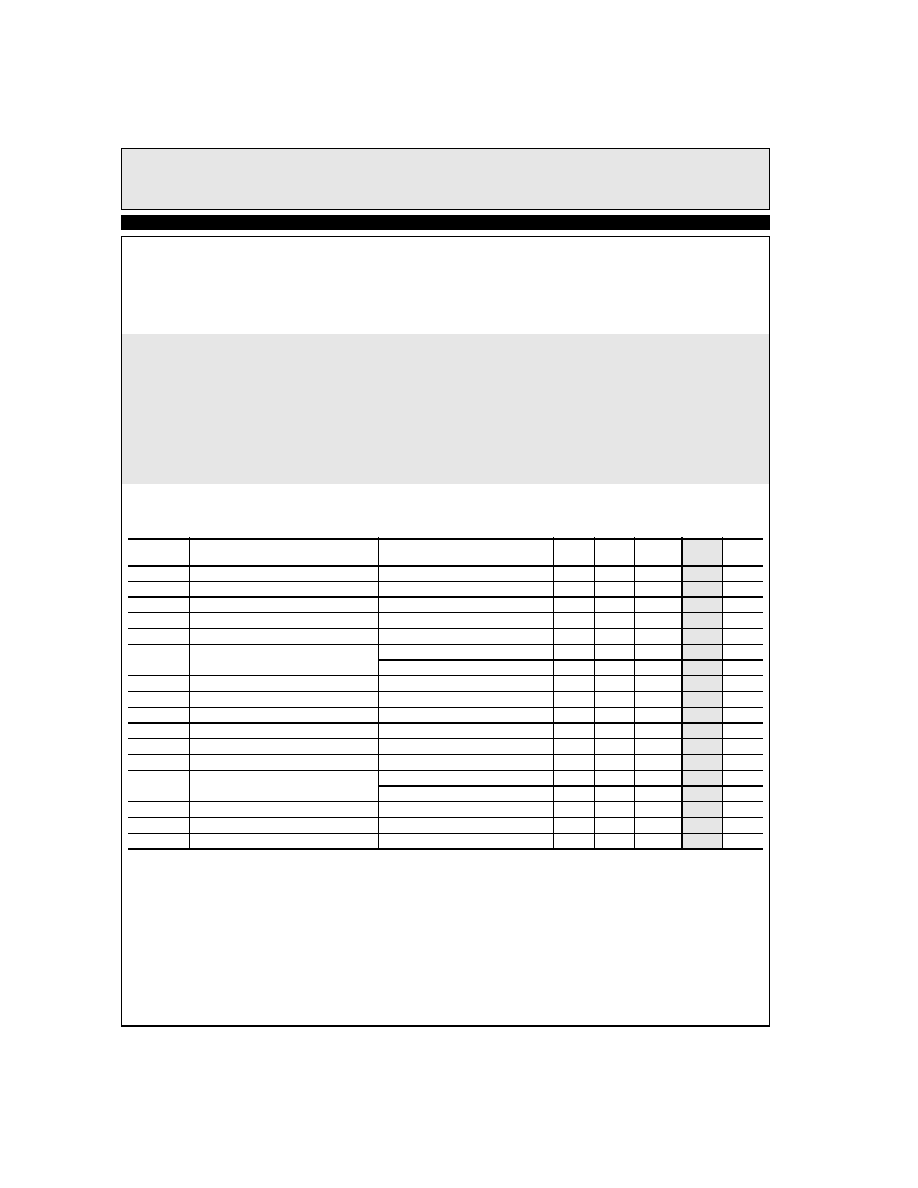
DC Characteristics
V
S
=+5V, R
L
=1K
, V
IN
=1V, T
A
=25∞C unless otherwise specified.
Parameter
Description
Conditions
Min
Typ
Max
Test
Level
Units
V
OS
Input Offset Voltage
-20
10
20
I
mV
TCV
OS
Average Offset Voltage Drift
[1]
-50
V
µ V/∞C
I
B
Input Bias Current
-15
-7
-3
I
µA
I
OS
Input Offset Current
0.3
1.0
I
µA
TCI
OS
Average Offset Current Drift
[1]
-1
-3
V
nA/∞C
A
VOL
Open Loop Gain
V
OUT=.
.5, 2.5, R
L
= 1K
160
250
I
V/V
V
OUT=.
.5, 2.5, R
L
= 150K
160
250
V
V/V
PSRR
Power Supply Rejection Ratio
V
S
= 4.5V to 5.5V
43
50
I
dB
CMRR
Common Mode Rejection Ratio
VCM = 0V to +3.8V
55
65
I
dB
CMIR
Common Mode Input Range
0.0
3.0
I
V
V
OUT
Output Voltage Swing
RFB = R
G
= 1K, R
L
= 150
2.8
3.2
I
V
I
SC
Output Short Circuit Current
Output to Ground
[2]
75
125
I
mA
I
S
Supply Current
No Load (per channel) V
IN
= 0V
2.0
2.4
3.0
I
mA
R
IN
Input Resistance
Differential
150
V
K
Common Mode
1.5
V
M
C
IN
Input Capacitance
A
V
= +1 @ 10 MHz
1
V
pF
R
OUT
Output Resistance
0.150
V
PSOR
Power Supply Operating Range
Single Supply
4
6
V
V

3
EL2320C
Triple, Low Cost, Gain of 1, Video Op Amp
EL
2320C
1.
For V
S
= 5V, V
OUT
= 4V
pp
. Full power bandwidth is based on slew rate measurement using: FPBW = SR/(2pi*V
peak
)
2.
Video performance measured at V
S
= 5V, A
V
= +2 with 2 times normal video level across R
L
= 150
Closed Loop AC Electrical Characteristics
V
S
=5V, AC Test Figure, T
A
= 25∞C unless otherwise specified
Parameter
Description
Conditions
Min
Typ
Max
Test
Level
Units
BW
-3dB Bandwidth (V
OUT
= 0.4 mVp-p)
±0.1 dB Bandwidth (V
OUT
= 0.4 mVp-p)
A
V
= +1
100
V
MHz
A
V
= +1
10
V
MHz
GBWP
Gain Bandwith Product
50
V
MHz
PM
Phase Margin
55
V
( ∞ )
SR
Slew Rate
85
130
V
V/µs
FBWP
Full Power Bandwidth
[1]
8
11
V
MHz
t
R
, t
F
Rise Time, Fall Time
0.1V step
2
V
ns
OS
Overshoot
0.1V step
15
V
%
t
PD
Propagation Delay
3.5
V
ns
t
S
Settling to 0.1% (A
V
= 1)
VS = 5V, 2V Step
80
V
ns
dG
Differential Gain
[2]
NTSC/PAL
0.1
V
%
dP
Differential Phase
[2]
NTSC/PAL
0.2
V
( ∞ )
e
N
Input Noise Voltage
10 KHz
15
V
nV/rt
(Hz)
i
N
Input Noise Current
10 KHz
1.5
V
nV/rt
(Hz)
CS
Channel Separation
P = 5 MHz
55
V
dB
4
EL2320C
Triple, Low Cost, Gain of 1, Video Op Amp
E
L
2320C
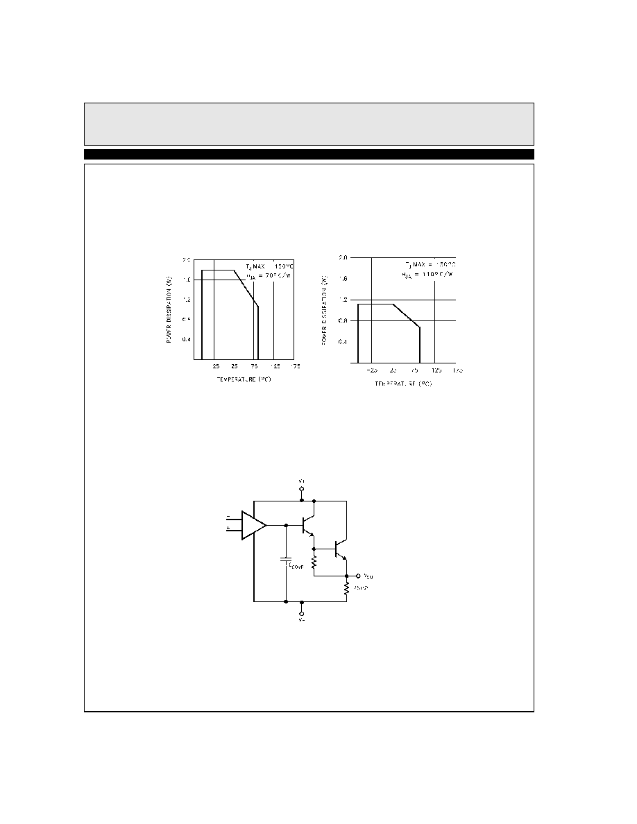
Typical Performance Curves
Simplified Block Diagram
14-Pin Plastic DIP
Maximum Power Dissipation
vs Ambient Temperature
14-Lead SO
Maximum Power Dissipation
vs Ambient Temperature

5
EL2320C
Triple, Low Cost, Gain of 1, Video Op Amp
EL
2320C
Applications Information
Product Description
The EL2320C operational amplifier is stable at a gain of
1. It is built on Elantec's proprietary complimentary
bipolar process. This topology allows it to be used in a
variety of applications where current mode amplifiers
are not appropriate because of restrictions placed on the
feedback elements. This product is especially designed
for applications where high bandwidth and good video
performance characteristics are desired but the higher
cost of more flexible and sophisticated products are
prohibitive.
Power Supplies
The EL2320C is designed to work at a supply voltage
difference of 4.5V to 5.5V. It will work on any combina-
tion of ± supplies. All electrical characteristics are
measured with a 5V supply.
Output Swing vs Load
Please refer to the simplified block diagram. This ampli-
fier provides an NPN pull-up transistor output and a
passive 1250
pull-down resistor to the most negative
supply. In a application where the load is connected to
V
S
-
the output voltage can swing to within 200 mV of
V
S
- .
Output Drive Capability
This device does not have short circuit protection. Each
output is capable of than 100 mA into a shorted output.
Care must be used in the design to limit the output cur-
rent with a series resistor.
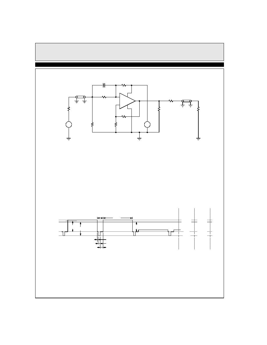
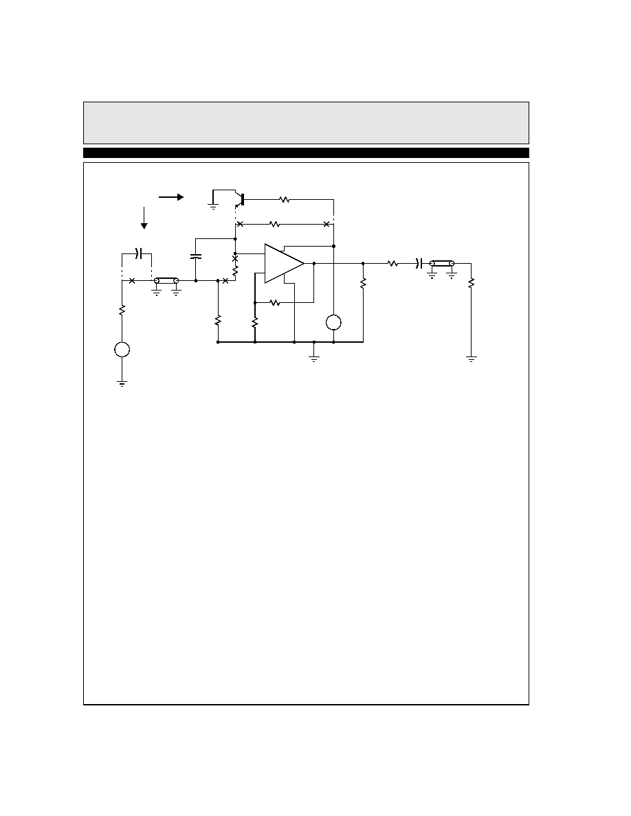
Single 5 Volt Supply Video Cable Driver
These amplifiers may be used as a direct coupled video
cable driver with a gain of 2. With a 75
back matching
resistor driving a terminated 75
cable the output at the
cable load will be original video level (1V NTSC). The
best operating mode is with direct coupling. The input
signal must be offset to keep the entire signal within the
range of the amplifier. The required offset voltage can
be set with a resistor divider and a bypass capacitor in
the video path (Figure 1). The input DC offset should be
between .3V and .5V. With R
A
=68K and R
B
=4.7K the
input offset will be .32V. Since these amplifiers require
a DC load at their outputs it is good design practice to
add a 250
resistor to ground directly at the amplifier
output. Then if the 75
cable termination resistor were
inadvertently removed there would still be an output sig-
nal. The values in figure 1 give an output range of 0V to
2.6V
Output capacitive coupling also has some restrictions.
These amplifiers require a DC load at their outputs. A
75
back matching resistor to a cable and a 75
load to
ground at the end of the cable provide a 150
DC load.
But output capacitive coupling opens this DC path so an
extra pulldown resistor on the amplifier output to ground
is required. Figure 4 shows a 250
resistor. Capacitively
coupling the output will require that we shift the output
offset voltage higher than in the direct coupled case.
Using R
A
=43K and R
B
=4.7K will make the quiescent
output offset voltage about 1V. The output dynamic
range will be .6V to 3V.
6
EL2320C
Triple, Low Cost, Gain of 1, Video Op Amp
E
L
2320C
Input capacitive coupling will increase the needed
dynamic range of the amplifier. The standard NTSC
video signal is 1V peak to peak plus 143 mV for the
color AC peak. The video signal is made up of the -286
mV sync pulse plus the 714 mV picture signal which
may very from 0V to 714 mV. The video signal average
value for a black picture is about 28 mV (Figure 2) and
with a white picture level is about 583 mV (Figure 3).
This gives a maximum change in average value of about
555 mV. A direct coupled amplifier with an standard
NTSC video signal needs a dynamic range of 1.143V.
But with input capacitance coupling the dynamic range
requirements are the sum of the 1.143V video plus the
average picture value change of 0.555V or 1.698V
P-P
.
At a gain of two this doubles to 3.394V. These amplifi-
ers do not have this much dynamic range so a gain of
less than 2 must be used to avoid waveform compression
under all conditions.
+
≠
Video
1 V
75
RIS
V IN
RIL
4.7K
75
RB
+
-
AMP
1K
RF
1K
RG
0.1 µF
CB
68K
RA
0.32 VB
+
≠
V1
5 V
0.64 VB
250
RPD
V AMP
V OUT
75
RCL
75
RO
1 V
Figure 1.
0.714 V
0.0 V
-0.286 V
ð10
5.1 µs
3.8 µs
1.3 µs
53 µs
0.6
0.867
0.583 V
Gain = 2
1.8 V offset
Amp Out
Volts
0
+0.348
1.166
1.8
1.428
2.062
-0.572
+0.062
Figure 2. White Level Video
7
EL2320C
Triple, Low Cost, Gain of 1, Video Op Amp
EL
2320C
Capacitively coupling the input and output is worse than
a capacitor only on the input. Without any special com-
promises you can only take a gain of one. But if the
backmatch resistor is reduced to 36
, reducing the out-
put range requirement 25% and the output offset is
shifted to 2.1V you can take a gain of 1.5 and have a
standard NTSC 1Vat the 75
load.
A simple transistor, capacitor and resistor sync tip clamp
may be used when the input is already AC coupled to set
the sync tip to ground.This gives the input a fixed DC
level and can be used like a direct coupled input. The
clamp uses a PNP transistor with the collector at ground
and the base has a 200 K
resistor to 5V. The emitter-
connects to the amplifier input and a capacitor from the
video input. The clamp functions as an inverted Beta
current source for input bias current with plus inputs and
a clamp to ground for minus inputs. The R
A
and R
B
resistors are removed for the clamp option (Figure 4).
Printed Circuit Layout
The EL2320C is well behaved, and easy to apply in most
applications. However, a few simple techniques will
help assure rapid, high quality results. As with any high
frequency device, good PCB layout is necessary for
optimum performance. Ground-plane construction is
highly recommended, as is good power supply bypass-
ing. A 0.1 µ F ceramic capacitor is recommended for
bypassing both supplies. Lead lengths should be as short
as possible, and bypass capacitors should be as close to
the device pins as possible. For good AC performance,
parasitic capacitances should be kept to a minimum at
both inputs and at the output. Resistor values should be
kept under 5 K
because of the RC time constants asso-
ciated with the parasitic capacitance. Metal-film and
carbon resistors are both acceptable, use of wire-wound
resistors is not recommended because of their parasitic
inductance. Similarly, capacitors should be low-induc-
tance for best performance.
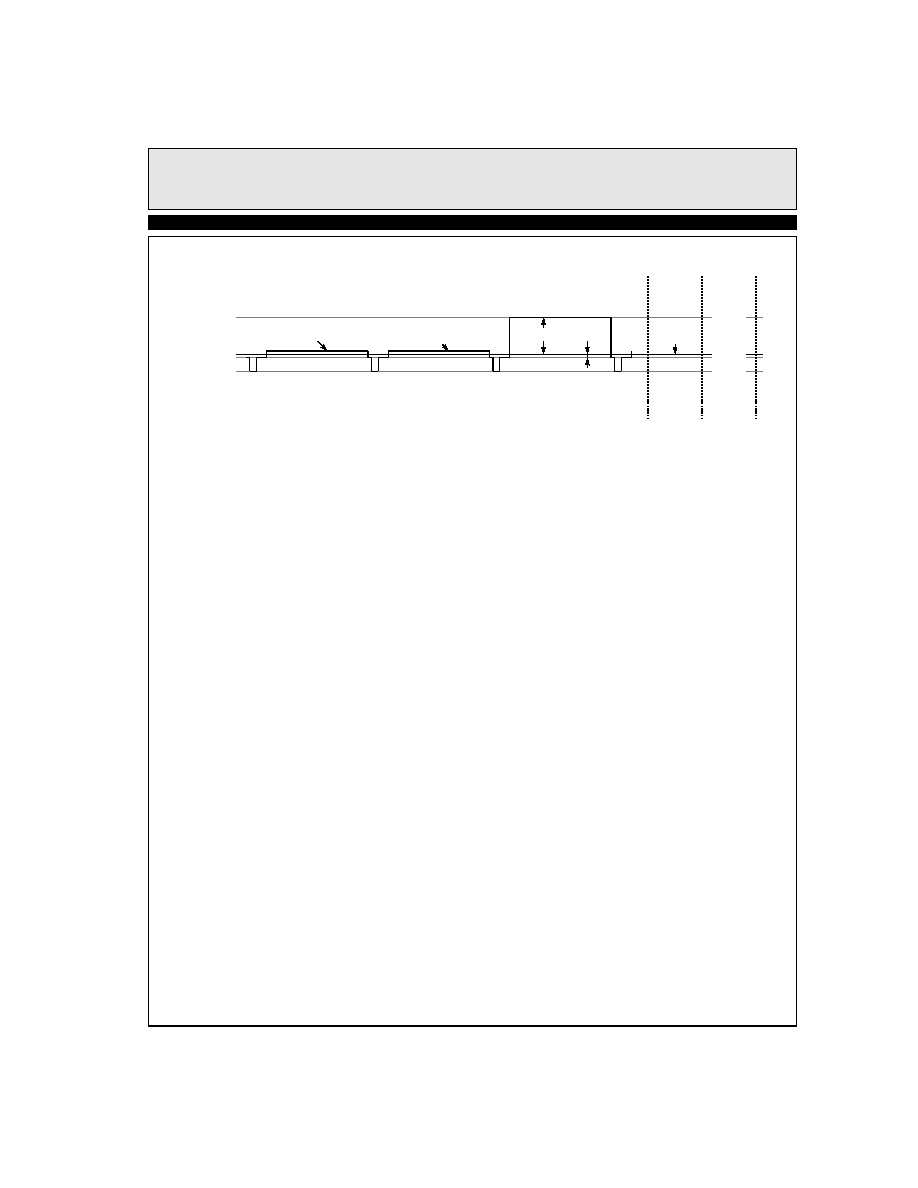
0.714 V
0.0 V
-0.286 V
Gain = 2
1.8 V offset
Amp Out
Volts
+1.8
+3.172
+56 mV
+1.172
Figure 3. Black Level Video
53 mV
Average BL
+45 mV
0.686 V
+28 mV
Average Picture Value Change -- 555 mV
8
EL2320C
Triple, Low Cost, Gain of 1, Video Op Amp
E
L
2320C
+
≠
Video
1 V
75
RIS
V IN
RIL
200K
75
RC
+
-
AMP
1K
RF
2K
RG
47 µF
CI
12K
RA
+
≠
V1
5 V
2.1VB
25
0
RPD
V AMP
V OUT
75
RC
L
36
RO
1 V
Figure 4.
PNP
1.4VB
0.
1
µF
RB
CB
4.7
K
47 µF
CO
Clamp
Option
2N3904

9
EL2320C
Triple, Low Cost, Gain of 1, Video Op Amp
EL
2320C

10
EL2320C
Triple, Low Cost, Gain of 1, Video Op Amp
E
L
2320C
General Disclaimer
Specifications contained in this data sheet are in effect as of the publication date shown. Elantec, Inc. reserves the right to make changes in the cir-
cuitry or specifications contained herein at any time without notice. Elantec, Inc. assumes no responsibility for the use of any circuits described
herein and makes no representations that they are free from patent infringement.
WARNING - Life Support Policy
Elantec, Inc. products are not authorized for and should not be used
within Life Support Systems without the specific written consent of
Elantec, Inc. Life Support systems are equipment intended to sup-
port or sustain life and whose failure to perform when properly used
in accordance with instructions provided can be reasonably
expected to result in significant personal injury or death. Users con-
templating application of Elantec, Inc. Products in Life Support
Systems are requested to contact Elantec, Inc. factory headquarters
to establish suitable terms & conditions for these applications. Elan-
tec, Inc.'s warranty is limited to replacement of defective
components and does not cover injury to persons or property or
other consequential damages.
Elantec, Inc.
1996 Tarob Court
Milpitas, CA 95035
Telephone: (408) 945-1323
(800) 333-6314
Fax:
(408) 945-9305
European Office: 44-71-482-4596
February 1997 Re
v A
Printed in U.S.A.