EL2386C
June
1996
Rev
A
EL2386C
250 MHz Triple Current Feedback Amp w Disable
Note All information contained in this data sheet has been carefully checked and is believed to be accurate as of the date of publication however this data sheet cannot be a ``controlled document'' Current revisions if any to these
specifications are maintained at the factory and are available upon your request We recommend checking the revision level before finalization of your design documentation
1996 Elantec Inc
Features
Triple amplifier topology
3 mA supply current (per
amplifier)
250 MHz
b
3 dB bandwidth
Low cost
Fast disable
Powers down to 0 mA
Single- and dual-supply
operation down to
g
1 5V
0 05% 0 05 Diff gain Diff
phase into 150
X
1200V ms slew rate
Large output drive current
55 mA
Available in single (EL2186C)
and dual (EL2286C) form
Non-power down versions
available in single dual and quad
(EL2180C EL2280C EL2480C)
Lower power EL2170C EL2176C
family also available
(1 mA 70 MHz) in single dual
and quad
Applications
Low power battery applications
HDSL amplifiers
Video amplifiers
Cable drivers
RGB amplifiers
Test equipment amplifiers
Current to voltage converters
Multiplexing
Video broadcast equipment
Ordering Information
Part No
Temp Range
Package
Outline
EL2386CN
b
40 C to
a
85 C 16-Pin PDIP MDP0031
EL2386CS
b
40 C to
a
85 C 16-Pin SOIC MDP0027
General Description
The EL2386C is a triple current-feedback operational amplifier
which achieves a
b
3 dB bandwidth of 250 MHz at a gain of
a
1
while consuming only 3 mA of supply current per amplifier It
will operate with dual supplies ranging from
g
1 5V to
g
6V or
from single supplies ranging from
a
3V to
a
12V The EL2386C
also includes a disable power-down feature which reduces cur-
rent consumption to 0 mA while placing the amplifier output in
a high impedance state In spite of its low supply current the
EL2386C can output 55 mA while swinging to
g
4V on
g
5V
supplies
These attributes make the EL2386C an excellent
choice for low power and or low voltage cable-driver HDSL or
RGB applications
For Single and Dual applications
consider the EL2186C
EL2286C For Single Dual and Quad applications without dis-
able consider the EL2180C EL2280C or EL2480C all in indus-
try standard pin outs The EL2180C also is available in the tiny
SOT-23 package which is 28% the size of an SO8 package For
lower power applications where speed is still a concern consider
the EL2170C EL2176C family which also comes in similar Sin-
gle Dual and Quad configurations The EL2170C EL2176C
family provides a
b
3 dB bandwidth of 70 MHz while consum-
ing 1 mA of supply current per amplifier
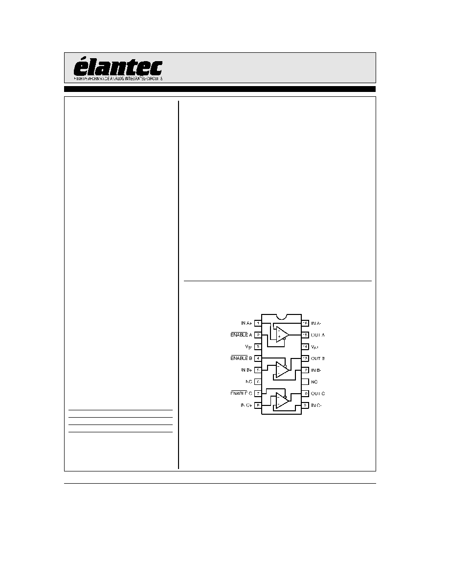
Connection Diagram
EL2386C SO P-DIP
2386-1
Top View
Manufactured under U S Patent No 5 418 495
EL2386C
250 MHz Triple Current Feedback Amp w Disable
Absolute Maximum Ratings
(T
A
e
25 C)
Voltage between V
Sa
and V
Sb
a
12 6V
Common-Mode Input Voltage
V
Sb
to V
Sa
Differential Input Voltage
g
6V
Current into
a
IN or
b
IN
g
7 5 mA
Internal Power Dissipation
See Curves
Operating Ambient Temperature Range
b
40 C to
a
85 C
Operating Junction Temperature
150 C
Output Current
g
60 mA
Storage Temperature Range
b
65 C to
a
150 C
Important Note
All parameters having Min Max specifications are guaranteed The Test Level column indicates the specific device testing actually
performed during production and Quality inspection Elantec performs most electrical tests using modern high-speed automatic test
equipment specifically the LTX77 Series system Unless otherwise noted all tests are pulsed tests therefore T
J
e
T
C
e
T
A
Test Level
Test Procedure
I
100% production tested and QA sample tested per QA test plan QCX0002
II
100% production tested at T
A
e
25 C and QA sample tested at T
A
e
25 C
T
MAX
and T
MIN
per QA test plan QCX0002
III
QA sample tested per QA test plan QCX0002
IV
Parameter is guaranteed (but not tested) by Design and Characterization Data
V
Parameter is typical value at T
A
e
25 C for information purposes only
DC Electrical Characteristics
V
S
e
g
5V R
L
e
150
X ENABLE
e
0V T
A
e
25 C unless otherwise specified
Parameter
Description
Conditions
Min
Typ
Max
Test
Units
Level
V
OS
Input Offset Voltage
2 5
15
I
mV
TCV
OS
Average Input Offset Voltage Drift
Measured from T
MIN
to T
MAX
5
V
mV C
dV
OS
VOS Matching
0 5
V
mV
a
I
IN
a
Input Current
1 5
15
I
mA
d
a
I
IN
a
I
IN
Matching
20
V
nA
b
I
IN
b
Input Current
16
40
I
mA
d
b
I
IN
b
I
IN
Matching
2
V
mA
CMRR
Common Mode Rejection Ratio
V
CM
e
g
3 5V
45
50
I
dB
b
ICMR
b
Input Current Common Mode Rejection
V
CM
e
g
3 5V
5
30
I
mA V
PSRR
Power Supply Rejection Ratio
V
S
e
g
4V to
g
6V
60
70
I
dB
b
IPSR
b
Input Current Power Supply Rejection
V
S
e
g
4V to
g
6V
1
15
I
mA V
R
OL
Transimpedance
V
OUT
e
g
2 5V
120
300
I
k
X
a
R
IN
a
Input Resistance
V
CM
e
g
3 5V
0 5
2
I
M
X
a
C
IN
a
Input Capacitance
1 2
V
pF
CMIR
Common Mode Input Range
g
3 5
g
4 0
I
V
V
O
Output Voltage Swing
V
S
e
g
5V
g
3 5
g
4 0
I
V
V
S
e a
5V Single-Supply High
4 0
V
V
V
S
e a
5V Single-Supply Low
0 3
V
V
I
O
Output Current
50
55
I
mA
2
TD
is
39in
EL2386C
250 MHz Triple Current Feedback Amp w Disable
DC Electrical Characteristics
V
S
e
g
5V R
L
e
150
X ENABLE
e
0V T
A
e
25 C unless otherwise specified
Contd
Parameter
Description
Conditions
Min
Typ
Max
Test
Units
Level
I
S
Supply Current
Enabled (per amplifier)
ENABLE
e
2 0V
3
6
I
mA
I
S(DIS)
Supply Current
Disabled (per amplifier)
ENABLE
e
4 5V
0
50
I
mA
C
OUT(DIS)
Output Capacitance
Disabled
ENABLE
e
4 5V
4 4
V
pF
R
IN-EN
ENABLE Pin Input Resistance
ENABLE
e
2 0V to 4 5V
45
85
I
k
X
I
IH-EN
ENABLE Pin Input Current
High
ENABLE
e
4 5V
b
0 04
V
mA
I
IL-EN
ENABLE Pin Input Current
Low
ENABLE
e
0V
b
53
V
mA
V
DIS
Minimum Voltage at ENABLE to Disable
4 5
I
V
V
EN
Maximum Voltage at ENABLE to Enable
2 0
I
V
AC Electrical Characteristics
V
S
e
g
5V R
F
e
R
G
e
750
X R
L
e
150
X ENABLE
e
0V T
A
e
25 C unless otherwise specified
Parameter
Description
Conditions
Min
Typ
Max
Test
Units
Level
BW
b
3 dB Bandwidth
A
V
e a
1
250
V
MHz
A
V
e a
2
180
V
MHz
BW
g
0 1 dB Bandwidth
A
V
e a
2
50
V
MHz
SR
Slew Rate
V
OUT
e
g
2 5V Measured at
g
1 25V
600
1200
IV
V
ms
t
R
t
F
Rise and Fall Time
V
OUT
e
g
500 mV
1 5
V
ns
t
PD
Propagation Delay
V
OUT
e
g
500 mV
1 5
V
ns
OS
Overshoot
V
OUT
e
g
500 mV
3 0
V
%
t
S
0 1% Settling
V
OUT
e
g
2 5V A
V
e b
1
15
V
ns
dG
Differential Gain (Note 1)
A
V
e a
2 R
L
e
150
X
0 05
V
%
dP
Differential Phase (Note 1)
A
V
e a
2 R
L
e
150
X
0 05
V
dG
Differential Gain (Note 1)
A
V
e a
1 R
L
e
500
X
0 01
V
%
dP
Differential Phase (Note 1)
A
V
e a
1 R
L
e
500
X
0 01
V
t
ON
Turn-On Time (Note 2)
A
V
e a
2 V
IN
e a
1V R
L
e
150
X
40
100
I
ns
t
OFF
Turn-Off Time (Note 2)
A
V
e a
2 V
IN
e a
1V R
L
e
150
X
800
2000
I
ns
CS
Channel Separation
f
e
5 MHz
85
V
dB
Note 1 DC offset from 0V to 0 714V AC amplitude 286 mV
p-p
f
e
3 58 MHz
Note 2 Measured from the application of the logic signal until the output voltage is at the 50% point between initial and final
values
3
TD
is
18in
TD
is
31in
EL2386C
250 MHz Triple Current Feedback Amp w Disable
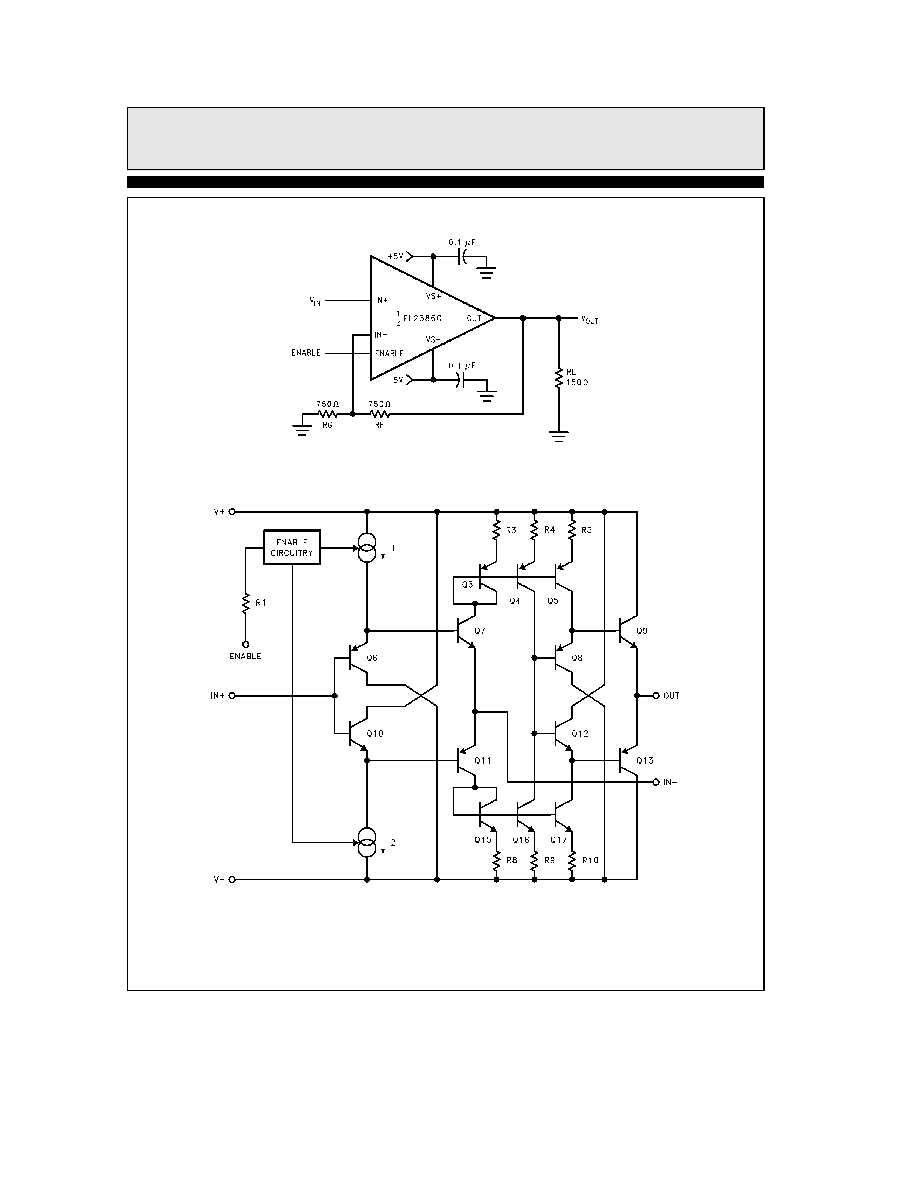
Test Circuit (per Amplifier)
2386-2
Simplified Schematic (per Amplifier)
2386-3
4
EL2386C
250 MHz Triple Current Feedback Amp w Disable
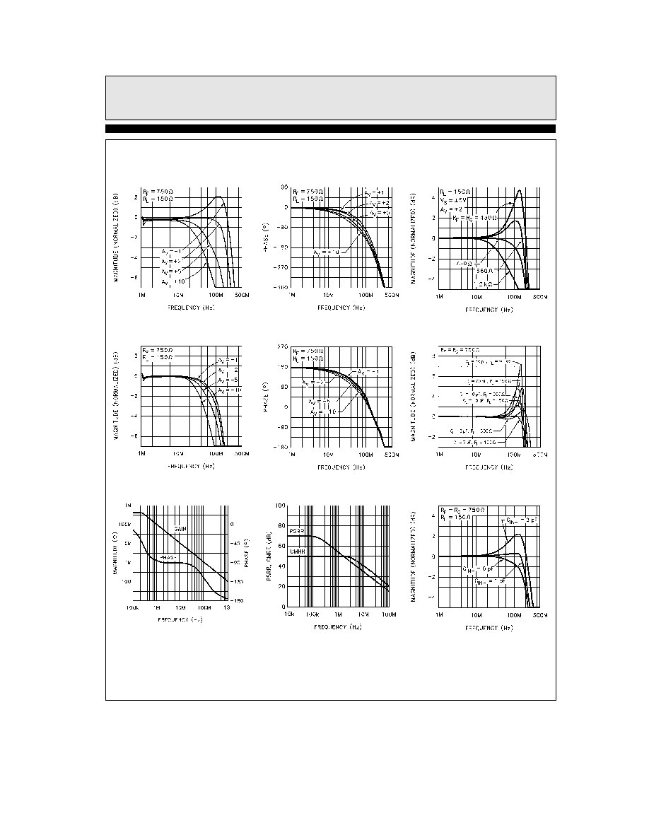
Typical Performance Curves
Contd
Response (Gain)
Non-Inverting Frequency
2386-4
Response (Phase)
Non-Inverting Frequency
2386-5
for Various R
F
and R
G
Frequency Response
2386-6
Response (Gain)
Inverting Frequency
2386-7
Response (Phase)
Inverting Frequency
2386-8
for Various R
L
and C
L
Frequency Response
2386-9
vs Frequency
Transimpedance (R
OL
)
2386-10
vs Frequency
PSRR and CMRR
2386-11
Various C
IN
b
Frequency Response for
2386-12
5