 | –≠–ª–µ–∫—Ç—Ä–æ–Ω–Ω—ã–π –∫–æ–º–ø–æ–Ω–µ–Ω—Ç: EL4083CN | –°–∫–∞—á–∞—Ç—å:  PDF PDF  ZIP ZIP |
EL4083C
December
1995
Rev
B
EL4083C
Current Mode Four Quadrant Multiplier
Note All information contained in this data sheet has been carefully checked and is believed to be accurate as of the date of publication however this data sheet cannot be a ``controlled document'' Current revisions if any to these
specifications are maintained at the factory and are available upon your request We recommend checking the revision level before finalization of your design documentation
1993 Elantec Inc
Features
Novel current mode design
Virtual ground current summing
inputs
Differential ground referenced
current outputs
High speed (both inputs)
200 MHz bandwidth
12 ns 1% settling time
Low distortion
THD
k
0 03%
1 MHz
THD
k
0 1%
10 MHz
Low noise (R
L
e
50
X)
100 dB dynamic range
10 Hz to 20 kHz
73 dB dynamic range
10 Hz to 10 MHz
Wide supply conditions
g
5 to
g
15V operation
Programmable bias current
0 2 dB gain tolerance to 25 MHz
Applications
Four quadrant multiplication
Gain control
Controlled signal summing and
multiplexing
HDTV video fading and
switching
Mixing modulating
demodulating (phase detection)
Frequency doubling
Division
Squaring
Square rooting
RMS and power measurement
Vector addition-RMS summing
CRT focus and geometry
correction
Polynomial function generation
AGC circuits
Ordering Information
Part No
Temp Range
Package
Outline
EL4083CN
b
40 C to
a
85 C
8-Pin P-DIP
MDP0031
EL4083CS
b
40 C to
a
85 C
8-Pin SO
MDP0027
General Description
The 4083C makes use of an Elantec fully complimentary oxide
isolated bipolar process to produce a patent pending current in
current out four quadrant multiplier Input and output signal
summing and direct interface to other current mode devices can
be accomplished by simple connection to reduce component
count and preserve bandwidth The selection of an appropriate
series resistor value allows an input to accept a voltage signal of
any size and optimize dynamic range The differential outputs
offer significant performance improvements which greatly ex-
tend the usable gain control range at high frequencies The bias
current is programmable to accommodate the voltage and pow-
er dissipation constraints of the package and available systems
supplies
The devices can implement all the classic four quadrant multi-
plier applications and are uniquely well suited to gain control
and signal summing of broadband signals
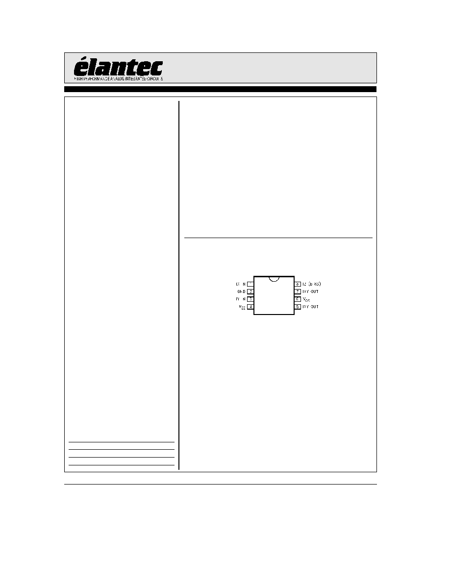
Connection Diagram
EL4083
8-Pin SO P DIP
4083 ≠ 1
Top View
Manufactured under U S Patent No 5 389 840
EL4083C
Current Mode Four Quadrant Multiplier
Absolute Maximum Ratings
(T
A
e
25 C)
V
S
Voltage between V
S
a
and V
S
b
a
33V
I
Z(BIAS)
Z Bias Current
a
2 4 mA
I
X
X Input Current
g
2 4 mA
I
Y
Y Input Current
g
2 4 mA
P
D
Maximum Power Dissipation
See Curves
T
A
Operating Temperature Range
EL4083
b
40 C to
a
85 C
T
J
Operating Junction Temperature
EL4083
150 C
T
ST
Storage Temperature
b
65 C to
a
150 C
Important Note
All parameters having Min Max specifications are guaranteed The Test Level column indicates the specific device testing actually
performed during production and Quality inspection Elantec performs most electrical tests using modern high-speed automatic test
equipment specifically the LTX77 Series system Unless otherwise noted all tests are pulsed tests therefore T
J
e
T
C
e
T
A
Test Level
Test Procedure
I
100% production tested and QA sample tested per QA test plan QCX0002
II
100% production tested at T
A
e
25 C and QA sample tested at T
A
e
25 C
T
MAX
and T
MIN
per QA test plan QCX0002
III
QA sample tested per QA test plan QCX0002
IV
Parameter is guaranteed (but not tested) by Design and Characterization Data
V
Parameter is typical value at T
A
e
25 C for information purposes only
Electrical Characteristics
(T
A
e
25 C V
S
e
g
5 I
Z
e
1 6 mA) unless otherwise specified
Parameter
Conditions
Min
Typ
Max
Test
Units
Level
Power Supplies
Operating Supply Voltage Range
g
4 5
g
16 5
I
V
I
CC
V
S
e
g
15V I
Z
e
0 2 mA
7 2
8 5
9 5
I
mA
I
CC
V
S
e
g
5V I
Z
e
1 6 mA
42 0
44 0
45
I
mA
I
EE
V
S
e
g
15V I
Z
e
0 2 mA
9 5
10 0
12
I
mA
I
EE
V
S
e
g
5V I
Z
e
1 6 mA
45
47
48
I
mA
Multiplier Performance
Transfer Function (Note 5)
(I
XY
≠ I
XY
)
e
K(I
X
c
I
Y
) I
Z
K Value
0 92
0 965
1 01
I
Total Error (Note 1)
b
2 mA
k
I
X
I
Y
k
2 mA
g
0 5
g
2
I
%FS
vs Temp
T
MIN
to T
MAX
g
1 5
g
3
IV
%FS
Linearity (Note 2)
0 25
0 5
I
%FS
Bandwidth (Note 3)
b
3 dB (See Figure 2)
200
225
III
MHz
X Feedthrough DC to I
XY
or I
XY
(Note 5)
I
X
e
g
2 mA I
Y
e
0 (unnulled)
0 15
1 6
I
%FS
Y Feedthrough DC to I
XY
or I
XY
(Note 5)
I
Y
e
g
2 mA I
X
e
0 (unnulled)
0 15
1 6
I
%FS
AC Feedthrough X to I
XY
or I
XY
(Note 4)
I
X
e
4 mApp I
Y
e
nulled
f
e
3 58 MHz
b
80
V
dB
f
e
100 MHz
b
28
V
dB
AC Feedthrough X to (I
XY
≠ I
XY
) (Note 4)
I
X
e
4 mApp I
Y
e
nulled
b
50
V
dB
DC
k
f
k
1 GHz
AC Feedthrough Y to I
XY
or I
XY
(Note 4)
I
Y
e
4 mApp I
X
e
nulled
f
e
3 58 MHz
b
64
V
dB
f
e
100 MHz
b
26
V
dB
AC Feedthrough Y to (I
XY
≠ I
XY
) (Note 4)
I
Y
e
4 mApp I
X
e
nulled
DC
k
f
k
1 GHz
b
50
V
dB
2
TD
is
37in

EL4083C
Current Mode Four Quadrant Multiplier
Electrical Characteristics
Contd
(T
A
e
25 C V
S
e
g
5 I
Z
e
1 6 mA) unless otherwise specified
Parameter
Conditions
Min
Typ
Max
Test
Units
Level
Inputs (I
X
I
Y
)
Full Scale Range
FRS
e
1 25
c
I
Z
(Nominal)
g
2
I
mA
Clipping Level
C
L
e
2
c
I
Z
2 85
3 2
I
mA
Z
IN
(I
X
)
30
40
48
I
X
Z
IN
(I
Y
)
30
36
48
I
X
Input Offset Voltages
at Input Pins I
Z
e
1 6 mA
b
4
a
4
mV
(V
OSX
V
OSY
)
I
Z
e
0 2 mA
b
12
a
12
mV
Input Offset Currents (Note 5)
R
SX
e
R
SY
e
1K V
X
e
V
Y
e
0
g
10
g
40
I
mA
I
XOS
I
YOS
T
MIN
to T
MAX
g
20
V
nA C
Nonlinearity
I
X
I
Y
e
2 mA
b
2 mA
k
I
X
k
2 mA
0 1
0 6
I
%FS
I
Y
I
X
e
2 mA
b
2 mA
k
I
Y
k
2 mA
0 1
0 4
I
%FS
Distortion I
X
(to I
XY
or I
XY
)
I
Y
e
2 mA
b
2 mA
k
I
X
k
2 mA
f
e
3 58 MHz
b
55
V
dB
f
e
100 MHz
b
25
V
dB
Distortion I
Y
(to I
XY
or I
XY
)
I
X
e
2 mA
b
2 mA
k
Iy
k
2 mA
f
e
3 58 MHz
b
56
V
dB
f
e
100 MHz
b
26
V
dB
Distortion I
X
(to (I
XY
b
I
XY
)
I
Y
e
2 mA
b
2 mA
k
I
X
k
2 mA
f
e
3 58 MHz
b
66
V
dB
f
e
100 MHz
b
35
V
dB
Distortion I
Y
(to (I
XY
b
I
XY
)
I
X
e
2 mA
b
2 mA
k
I
Y
k
2 mA
f
e
3 58 MHz
b
66
V
dB
f
e
100 MHz
b
34
V
dB
Diff Gain
3 58 MHz
I
X
I
Z
e
0 2 mA I
Y
e
0 25 mA
0 2
V
%
I
Y
I
Z
e
0 2 mA I
X
e
0 25 mA
0 17
V
%
I
X
I
Z
e
1 6 mA I
Y
e
2 mA
0 1
V
%
I
Y
I
Z
e
1 6 mA I
X
e
2 mA
0 05
V
%
Diff Phase
3 58 MHz
I
X
I
Z
e
0 2 mA I
Y
e
0 25 mA
0 5
V
deg
I
Y
I
Z
e
0 2 mA I
X
e
0 25 mA
0 5
V
deg
I
X
I
Z
e
1 6 mA I
Y
e
2 mA
0 05
V
deg
I
Y
I
Z
e
1 6 mA I
X
e
2 mA
0 05
V
deg
Outputs (I
XY
I
YX
)
Output I
OS
(Note 5)
I
X
e
I
Y
e
0
b
15
g
120
I
mA
Diff Output I
OS
(Note 5)
I
X
e
I
Y
e
0 (I
XY
≠ I
XY
)
g
0 1
g
80
I
mA
Voltage Compliance
g
1 5
g
2 0
V
V
Max Output Current Swing
g
2 85
g
3 2
I
mA
Noise Spectral Density
10 Hz
k
f
k
10 MHz
R
L
e
50
X
125
V
pA rootHz
I
Z
(Bias)
Current Range
Tested
0 2
1 6
I
mA
Input Voltage
I
Z
e
0 2 mA
g
25
I
mV
Input Voltage
I
Z
e
1 6 mA
g
25
I
mV
Note 1 Error is defined as the maximum deviation from the ideal transfer function expressed as a percentage of the full scale
output
Note 2 Linearity is defined as the error remaining after compensating for scale factor (gain) variation and input and output referred
offset errors
Note 3 Bandwidth is guaranteed using the squaring mode test circuit of Figure 4
Note 4 Relative to full scale output with full scale sinewave on signal input and zero port input nulled Specification represents
feedthrough of the fundamental
Note 5 Specifications are provisional for the EL4083
3
TD
is
58in
EL4083C
Current Mode Four Quadrant Multiplier
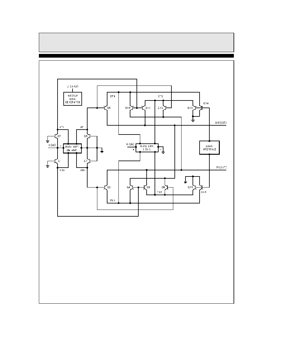
EL4083 Block Diagram
4083 ≠ 3
Figure 1
4

EL4083C
Current Mode Four Quadrant Multiplier
AC Test Fixture
4083 ≠ 4
Figure 2 AC Bandwidth Test Fixture
Burn-In Circuit
Top View
4083 ≠ 5
Figure 3 Burn-In Circuit P-DIP
5