 | –≠–ª–µ–∫—Ç—Ä–æ–Ω–Ω—ã–π –∫–æ–º–ø–æ–Ω–µ–Ω—Ç: EL4094C | –°–∫–∞—á–∞—Ç—å:  PDF PDF  ZIP ZIP |

EL4094C
August
1996
Rev
D
EL4094C
Video Gain Control Fader
Note All information contained in this data sheet has been carefully checked and is believed to be accurate as of the date of publication however this data sheet cannot be a ``controlled document'' Current revisions if any to these
specifications are maintained at the factory and are available upon your request We recommend checking the revision level before finalization of your design documentation
1993 Elantec Inc
Features
Complete video fader
0 02% 0 04 differential gain
phase
100% gain
Output amplifier included
Calibrated linear gain control
g
5V to
g
15V operation
60 MHz bandwidth
Low thermal errors
Applications
Video faders wipers
Gain control
Video text insertion
Level adjust
Modulation
Ordering Information
Part No
Temp Range
Package
Outline
EL4094CN
b
40 C to
a
85 C 8-Pin P-DIP MDP0031
EL4094CS
b
40 C to
a
85 C 8-Pin SO
MDP0027
General Description
The EL4094C is a complete two-input fader It combines two
inputs according to the equation
V
OUT
e
V
INA
(0 5V
a
Vg)
a
V
INB
(0 5V
b
Vg)
where V
GAIN
is the difference between V
GAIN
and V
GAIN
pin
voltages and ranges from
b
0 5V to
a
0 5V It has a wide 60
MHz bandwidth at
b
3 dB and is designed for excellent video
distortion performance The EL4094C is the same circuit as the
EL4095 but with feedback resistors included on-chip to imple-
ment unity-gain connection An output buffer is included in
both circuits
The gain-control input is also very fast with a 20 MHz small-
signal bandwidth and 70 ns recovery time from overdrive
The EL4094C is compatible with power supplies from
g
5V to
g
15V and is available in both the 8-pin plastic DIP and SO-8
Connection Diagram
4094 ≠ 1
Manufactured under U S Patent No 5 321 371 5 374 898
EL4094C
Video Gain Control Fader
Absolute Maximum Ratings
(T
A
e
25 C)
V
S
a
Voltage between V
S
a
and GND
a
18V
V
S
Voltage between V
S
a
and V
S
b
a
33V
V
INA
Input Voltage
(V
S
b
)
b
0 3V
V
INB
to (V
S
a
)
a
0 3V
V
GAIN
Input Voltage
V
GAIN
g
5V
V
GAIN
Input Voltage
V
S
b
to V
S
a
I
OUT
Output Current
g
35 mA
Internal Power Dissipation
See Curves
T
A
Operating Ambient Temp Range
b
40 C to
a
85 C
T
J
Operating Junction Temperature
150 C
T
ST
Storage Temperature Range
b
65 C to
a
150 C
Important Note
All parameters having Min Max specifications are guaranteed The Test Level column indicates the specific device testing actually
performed during production and Quality inspection Elantec performs most electrical tests using modern high-speed automatic test
equipment specifically the LTX77 Series system Unless otherwise noted all tests are pulsed tests therefore T
J
e
T
C
e
T
A
Test Level
Test Procedure
I
100% production tested and QA sample tested per QA test plan QCX0002
II
100% production tested at T
A
e
25 C and QA sample tested at T
A
e
25 C
T
MAX
and T
MIN
per QA test plan QCX0002
III
QA sample tested per QA test plan QCX0002
IV
Parameter is guaranteed (but not tested) by Design and Characterization Data
V
Parameter is typical value at T
A
e
25 C for information purposes only
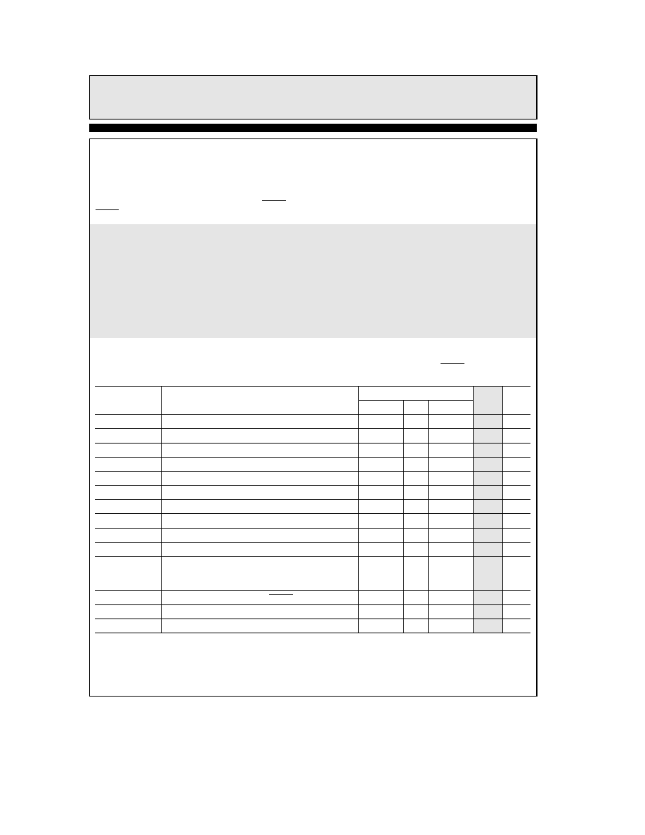
Open Loop DC Electrical Characteristics
V
S
e
g
5V T
A
e
25 C V
GAIN
e a
0 6V to measure channel A V
GAIN
e b
0 6V to measure channel B V
GAIN
e
0V unless
otherwise specified
Parameter
Description
Limits
Level
Test
Units
Min
Typ
Max
V
OS
Input Offset Voltage
4
30
I
mV
I
Ba
V
IN
Input Bias Current
2
10
I
mA
PSRR
Power Supply Rejection Ratio
60
80
I
dB
EG
Gain Error 100% Setting
b
0 5
b
0 8
I
%
V
IN
V
IN
Range
(V
b
)
a
2 5
(V
a
)
b
2 5
I
V
V
O
Output Voltage Swing
(V
b
)
a
2 5
(V
a
)
b
2 5
I
V
I
SC
Output Short-Circuit Current
50
95
150
I
mA
V
GAIN
100%
Minimum Voltage at V
GAIN
for 100% Gain
0 45
0 5
0 55
I
V
V
GAIN
0%
Maximum Voltage at V
GAIN
for 0% Gain
b
0 55
b
0 5
b
0 45
I
V
NL Gain
Gain Control Non-linearity V
IN
e
g
0 5V
1 5
4
I
%
NL A
V
e
1
Signal Non-linearity V
IN
e
0 to
g
1V V
GAIN
e
0 55V
0 01
V
%
A
V
e
0 5
Signal Non-linearity V
IN
e
0 to
g
1V V
GAIN
e
0V
0 05
V
%
A
V
e
0 25
Signal Non-linearity V
IN
e
0 to
g
1V V
GAIN
e b
0 25V
0 2
0 5
I
%
R
GAIN
Resistance between V
GAIN
and V
GAIN
4 6
5 5
6 6
I
k
X
I
S
Supply Current
12
14 5
19
I
mA
F
T
Off-Channel Feedthrough
b
75
b
50
I
dB
2
TD
is
06in
TD
is
33in

EL4094C
Video Gain Control Fader
Closed Loop AC Electrical Characteristics
V
S
e
g
15V C
L
e
15 pF T
A
e
25 C A
V
e
100% unless otherwise noted
Parameter
Description
Limits
Level
Test
Units
Min
Typ
Max
SR
Slew Rate V
OUT
from
b
3V to
a
3V measured at
b
2V and
a
2V
370
500
V
V
ms
BW
Bandwidth
b
3 dB
45
60
III
MHz
b
1 dB
35
V
MHz
b
0 1 dB
6
V
MHz
dG
Differential Gain AC amplitude of 286 mV
p-p
at 3 58 MHz on DC offset of
b
0 7 0 and
a
0 7V A
V
e
100%
0 02
V
%
A
V
e
50%
0 20
V
%
A
V
e
25%
0 40
V
%
d
i
Differential Phase AC ampitude of 286 mV
p-p
at 3 58 MHz on DC offset of
b
0 7 0 and
a
0 7V A
V
e
100%
0 04
V
( )
A
V
e
50%
0 20
V
( )
A
V
e
25%
0 20
V
( )
BW GAIN
b
3 dB Gain Control Bandwidth V
GAIN
Amplitude 0 5 V
p-p
20
V
MHz
T
REC
GAIN
Gain Control Recovery from Overload V
GAIN
from
b
0 6V to 0V
70
V
ns
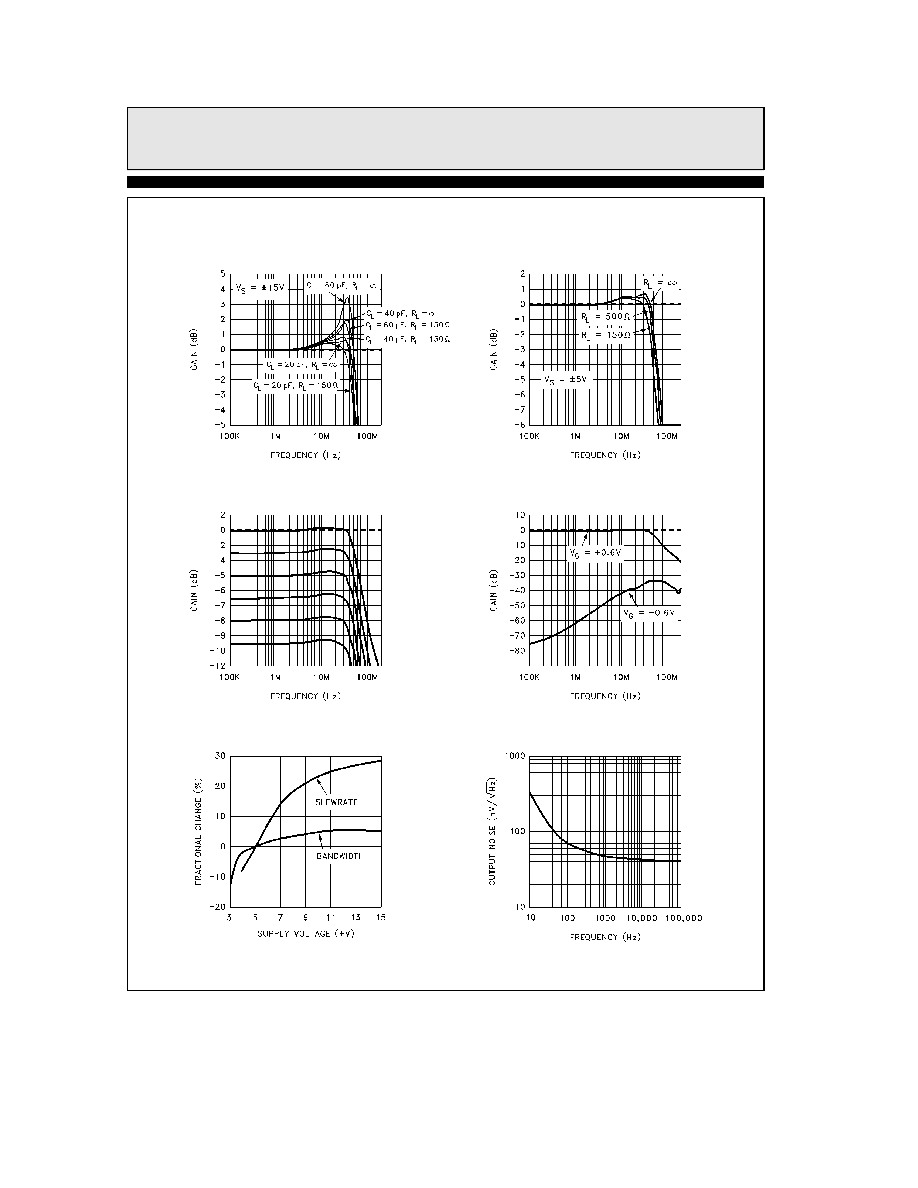
Typical Performance Curves
Small-Signal Step
Response for Gain e 100% 50%
25% and 0% V
S
g
5V
4094 ≠ 2
Large-Signal Step
Response for Gain e 100% 50%
25% and 0% V
S
g
12V
4094 ≠ 3
3
TD
is
26in
EL4094C
Video Gain Control Fader
Typical Performance Curves
Contd
Capacitive Loading
Frequency Response vs
Resistive Loading
Frequency Response vs
Frequency Response vs Gain
Over Frequency
Off-Channel Isolation
Bandwidth with Supply Voltage
Change in Slewrate and
Output Noise Over Frequency
4094 ≠ 4
4
EL4094C
Video Gain Control Fader
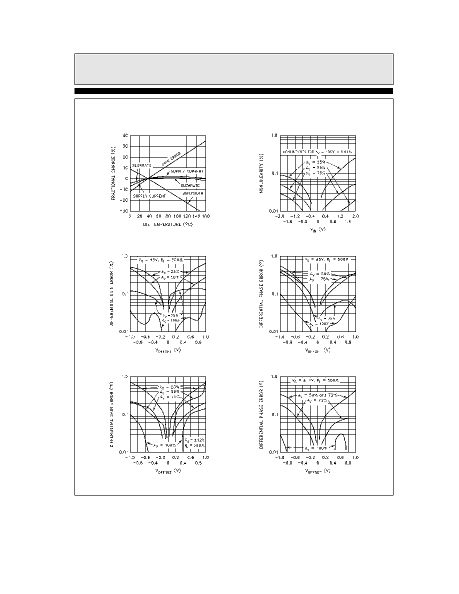
Typical Performance Curves
Contd
Bandwidth over Temperature
Supply Current Slewrate and
Change in 100% Gain Error
Gain e 100% 75% 50% and 25%
Nonlinearity vs V
IN
for
75% 50% and 25% F e 3 58 MHz
V
offset
for Gain e 100%
Differential Gain Error vs
75% 50% and 25% F e 3 58 MHz
V
offset
for Gain e 100%
Differential Phase Error vs
75% 50% and 25% F e 3 58 MHz
V
offset
for Gain e 100%
Differential Gain Error vs
75% 50% and 25% F e 3 58 MHz
V
offset
for Gain e 100%
Differential Phase Error vs
4094 ≠ 5
5