 | –≠–ª–µ–∫—Ç—Ä–æ–Ω–Ω—ã–π –∫–æ–º–ø–æ–Ω–µ–Ω—Ç: EL4348CU | –°–∫–∞—á–∞—Ç—å:  PDF PDF  ZIP ZIP |
Note: All information contained in this data sheet has been carefully checked and is believed to be accurate as of the date of publication; however, this data sheet cannot be a "controlled document". Current revisions, if any, to these
specifications are maintained at the factory and are available upon your request. We recommend checking the revision level before finalization of your design documentation.
© 2001 Elantec Semiconductor, Inc.
E
L
4
3
4
4
C
/
E
L
4
3
4
8
C
-
P
r
e
l
i
m
i
n
a
r
y
General Description
The EL4344C and EL4348C are 600MHz bandwidth multiplexing
amplifiers designed primarily for input video switching. The
EL4344C and EL4348C contain 4:1 multiplexing amplifiers.
The EN pin can be used to tri-state the MUX output, enabling parts to
be paralleded for a greater number of inputs. All logic inputs are refer-
enced to the GND pin.
The EL4344C has a gain of 1 and the EL4348C has a gain of 2.
The EL4344C and the EL4348C are available in a 28-pin QSOP pack-
age and are specified for operation over the full
--
-40∞C to +85∞C
temperature range.
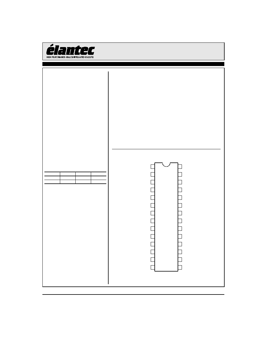
Connection Diagram
1
2
3
4
16
15
14
13
5
6
7
12
11
9
8
10
20
19
18
17
24
23
22
21
EL4344C & EL4348C
(28-Pin QSOP)
28
27
26
25
S0
IN3A
GND
GND
OUTA
OUTC
VS-
IN4C
GND
IN2A
IN1A
VS+
OUTB
IN4A
S1
IN1B
GND
IN2B
VS+
IN3B
VS-
IN4B
GND
IN1C
IN3C
GND
EN
IN2C
Features
∑ 4:1 Mux
∑ Triple channels
∑ ±5V operation
∑ Gain of 1 (EL4344C)
∑ Gain of 2 (EL4348C)
∑ 600MHz bandwidth
∑ Supply current of 11mA/channel
Applications
∑ HDTV/DTV Analog Inputs
∑ Video Projectors
∑ Computer Monitors
∑ Set Top Boxes
∑ Security Video
∑ Broadcast Video Equipment
Ordering Information
Part No.
Package
Tape & Reel
Outline #
EL4344CU
28-Pin QSOP
MDP0040
EL4348CU
28-Pin QSOP
MDP0040
EL4344C/EL4348C - Preliminary
600MHz Multiplexing Amplifiers
A
u
g
u
s
t
1
3
,
2
0
0
1
2
EL4344C/EL4348C - Preliminary
600MHz Multiplexing Amplifiers
E
L
4
3
4
4
C
/
E
L
4
3
4
8
C
-
P
r
e
l
i
m
i
n
a
r
y
Absolute Maximum Ratings
(T
A
= 25∞C)
Values beyond absolute maximum ratings can cause the device to be pre-
maturely damaged. Absolute maximum ratings are stress ratings only
and functional device operation is not implied.
Supply Voltage (V
S+
to V
S
-)
11V
Input Voltage
V
S
- - 0.3V, V
S+
+0.3V
Storage Temperature Range
-65∞C to +150∞C
Ambient Operating Temperature
-40∞C to +85∞C
Operating Junction Temperature
125∞C
Power Dissipation
See Curves
Important Note:
All parameters having Min/Max specifications are guaranteed. Typ values are for information purposes only. Unless otherwise noted, all tests are at the
specified temperature and are pulsed tests, therefore: T
J
= T
C
= T
A
.
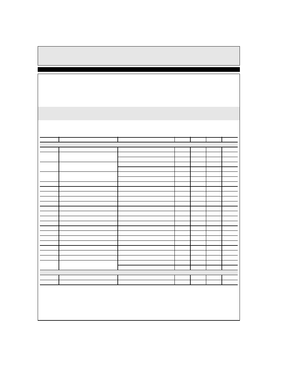
Specifications
V
S
= +5V, V
S
- = -5V, GND = 0V, T
A
= 25∞C, Input Video = 1V
P-P
& R
L
= 150
to GND, unless otherwise specified.
Parameter
Description
Conditions
Min
Typ
Max
Unit
General
I
S
Supply Current (per channel)
No load, V
IN
= 0V
16
18
mA
BW
-3dB Bandwidth
A
V
= 1 (EL4344C)
600
MHz
A
V
= 2 (EL4348C)
500
MHz
FBW
0.1dB Bandwidth
A
V
= 1 (EL4344C)
100
MHz
A
V
= 2 (EL4348C)
80
MHz
SR
Slew Rate
25% to 75%, R
L
= 150
, A
V
= 2 (EL4344C)
1200
V/µs
25% to 75%, R
L
= 150
, A
V
= 2 (EL4348C)
1400
V/µs
t
SW
Switching Time
10% to 90%
2
ns
V
OP
Positive Output Swing
3.3
3.5
V
V
ON
Negative Output Swing
-3.2
-3.5
V
I
OUT
Output Current
R
L
= 10
to GND
80
100
mA
dG
Differential Gain Error
Standard NTSC test, A
V
= 2, R
L
= 150
0.07
%
dP
Differential Phase Error
Standard NTSC test, A
V
= 2, R
L
= 150
0.01
∞
V
IN
Input Voltage (video inputs)
-2.8
2.3
V
V
OS
Offset Voltage
-10
10
mV
e
n
Voltage Noise
17
nV/
Hz
THD
Total Harmonic Distortion
V
OUT
= 2V
P-P
, R
L
= 150
, f = 200MHz
-70
dB
t
S
0.1% Settling Time
Step = 2V
6
ns
OS
Overshoot
Step = 2V
0.1
0.6
V
PSRR
Power Supply Rejection Ratio
50
dB
ISO
Channel Isolation
F = 30MHz
90
dB
V
GLITCH
Switching Glitch
70
120
mV
I
SDIS
Disable Supply Current
20
µA
A
V
Voltage Gain
EL4344C
1
EL4348C
2
Control
V
H
Logic Input High Voltage
2.0
V
V
L
Logic Input Low Voltage
0.8
V
3
EL4344C/EL4348C - Preliminary
600MHz Multiplexing Amplifiers
E
L
4
3
4
4
C
/
E
L
4
3
4
8
C
-
P
r
e
l
i
m
i
n
a
r
y
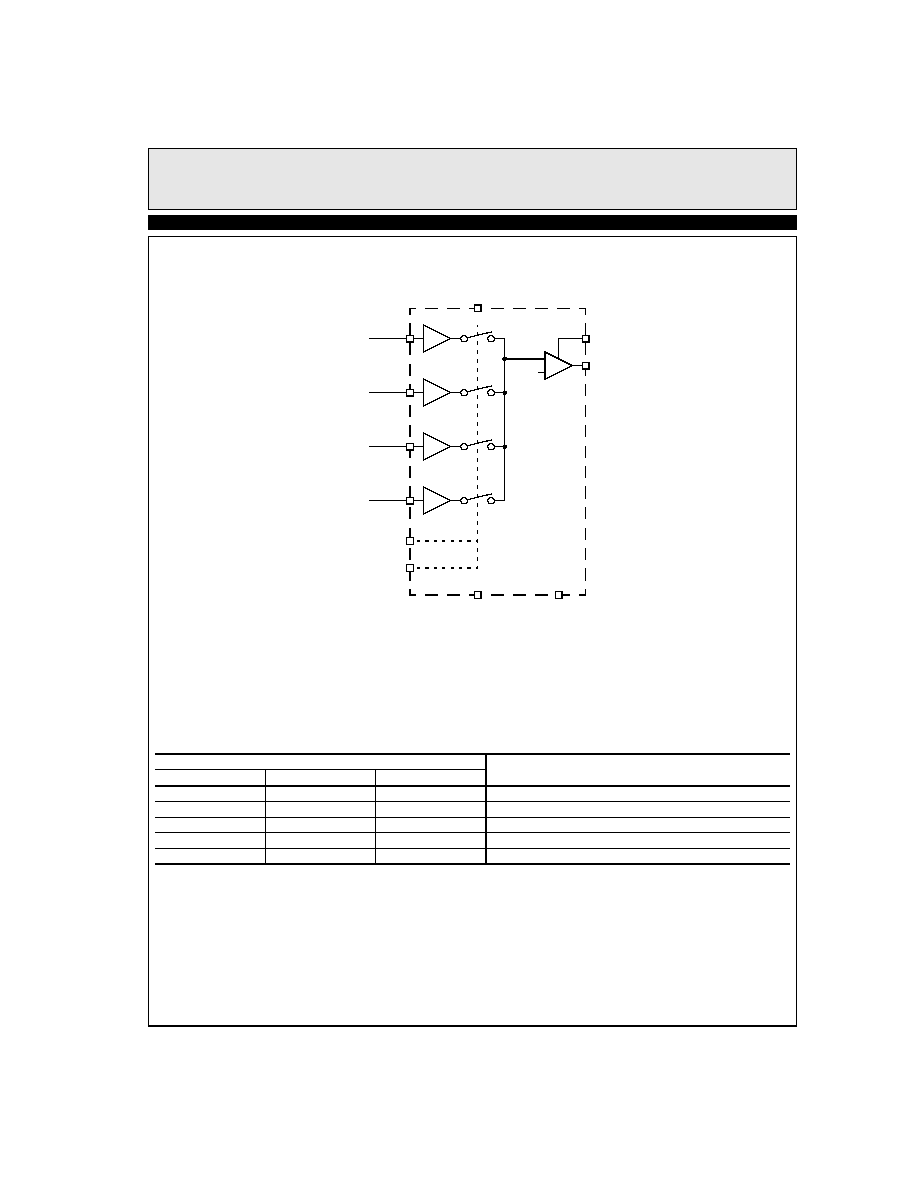
Block Diagram
-
+
V
S
+
GND
V
S
-
S
0
IN4
IN3
IN2
IN1
EN
OUT
Input Video
Input Video
Input Video
Input Video
S
1
Three channels - A, B & C
Input Selector Truth Table
Inputs
State
EN
S1
S0
1
0
0
IN1 Selected
1
0
1
IN2 Selected
1
1
0
IN3 Selected
1
1
1
IN4 Selected
0
X
X
Standby - Powered Down

4
EL4344C/EL4348C - Preliminary
600MHz Multiplexing Amplifiers
E
L
4
3
4
4
C
/
E
L
4
3
4
8
C
-
P
r
e
l
i
m
i
n
a
r
y
Pin Descriptions
Pin Number
Pin Name
Pin Type
Pin Description
1
S0
Logic Input
LSB for input selection
2
IN4A
High Frequency Signal
Input #4 for channel A
3
S1
Logic Input
MSB for input selection
4
IN1B
High Frequency Signal
Input #1 for channel B
5
GND
Power
Ground
6
IN2B
High Frequency Signal
Input #2 for channel B
7
VS+
Power
Positive power
8
IN3B
High Frequency Signal
Input #3 for channel B
9
VS-
Power
Negative power
10
IN4B
High Frequency Signal
Input #4 for channel B
11
GND
Power
Ground
12
IN1C
High Frequency Signal
Input #1 for channel C
13
EN
Logic Input
Logic high to enable
14
IN2C
High Frequency Signal
Input #2 for channel C
15
GND
Power
Ground
16
IN3C
High Frequency Signal
Input #3 for channel C
17
GND
Power
Ground
18
IN4C
High Frequency Signal
Input #4 for channel C
19
VS-
Power
Negative power
20
OUTC
High Frequency Signal
Output for channel C
21
OUTB
High Frequency Signal
Output for channel B
22
OUTA
High Frequency Signal
Output for channel A
23
VS+
Power
Positive power
24
IN1A
High Frequency Signal
Input #1 for channel A
25
GND
Power
Ground
26
IN2A
High Frequency Signal
Input #2 for channel A
27
GND
Power
Ground
28
IN3A
High Frequency Signal
Input #3 for channel A

5
EL4344C/EL4348C - Preliminary
600MHz Multiplexing Amplifiers
E
L
4
3
4
4
C
/
E
L
4
3
4
8
C
-
P
r
e
l
i
m
i
n
a
r
y
General Disclaimer
Specifications contained in this data sheet are in effect as of the publication date shown. Elantec, Inc. reserves the right to make changes in the cir-
cuitry or specifications contained herein at any time without notice. Elantec, Inc. assumes no responsibility for the use of any circuits described
herein and makes no representations that they are free from patent infringement.
WARNING - Life Support Policy
Elantec, Inc. products are not authorized for and should not be used
within Life Support Systems without the specific written consent of
Elantec, Inc. Life Support systems are equipment intended to sup-
port or sustain life and whose failure to perform when properly used
in accordance with instructions provided can be reasonably
expected to result in significant personal injury or death. Users con-
templating application of Elantec, Inc. Products in Life Support
Systems are requested to contact Elantec, Inc. factory headquarters
to establish suitable terms & conditions for these applications. Elan-
tec, Inc.'s warranty is limited to replacement of defective
components and does not cover injury to persons or property or
other consequential damages.
A
u
g
u
s
t
1
3
,
2
0
0
1
Printed in U.S.A.
Elantec Semiconductor, Inc.
675 Trade Zone Blvd.
Milpitas, CA 95035
Telephone: (408) 945-1323
(888) ELANTEC
Fax:
(408) 945-9305
European Office: +44-118-977-6020
Japan Technical Center: +81-45-682-5820