 | –≠–ª–µ–∫—Ç—Ä–æ–Ω–Ω—ã–π –∫–æ–º–ø–æ–Ω–µ–Ω—Ç: EL4390C | –°–∫–∞—á–∞—Ç—å:  PDF PDF  ZIP ZIP |
EL4390C
November
1994
Rev
A
EL4390C
Triple 80 MHz Video Amplifier with DC Restore
Note All information contained in this data sheet has been carefully checked and is believed to be accurate as of the date of publication however this data sheet cannot be a ``controlled document'' Current revisions if any to these
specifications are maintained at the factory and are available upon your request We recommend checking the revision level before finalization of your design documentation
1994 Elantec Inc
Features
80 MHz
b
3 dB bandwidth for
gains of 1 to 10
800 V ms slew rate
15 MHz bandwidth flat to 0 1 dB
Excellent differential gain and
phase
TTL CMOS compatible DC
restore function
Available in 16 lead P-DIP 16
lead SOL
Applications
RGB drivers requiring DC
restoration
RGB multiplexers requiring DC
restoration
RGB building blocks
Video gain blocks requiring DC
restoration
Sync and color burst processing
Ordering Information
Part No
Temp Range
Package
Outline
EL4390CN
b
40 C to
a
85 C 16-Pin P-DIP MDP0031
EL4390CM
b
40 C to
a
85 C 16-Lead SOL
MDP0027
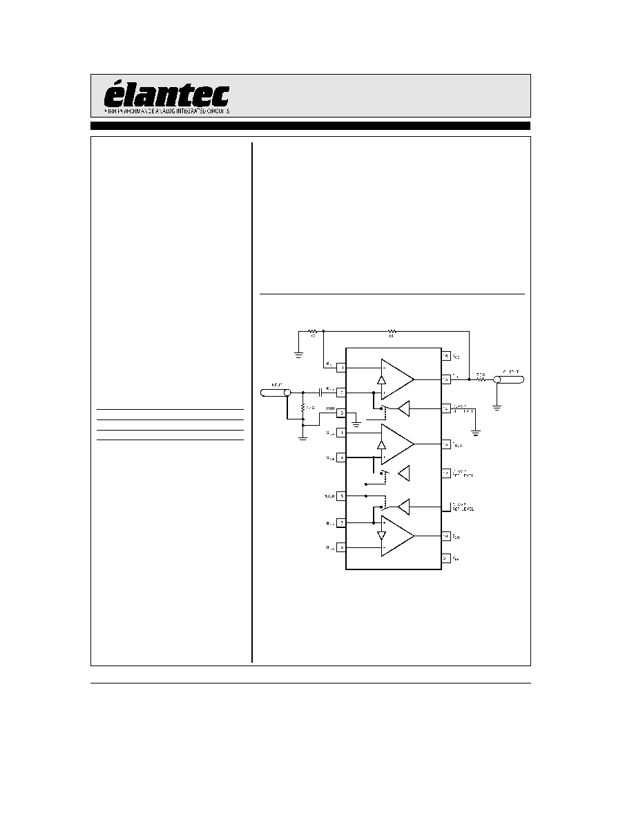
General Description
The EL4390C is three wideband current-mode feedback amplifi-
ers optimized for video performance each with a DC restore
amplifier The DC restore function is activated by a common
TTL CMOS compatible control signal while each channel has a
separate restore reference
Each amplifier can drive a load of 150
X at video signal levels
The EL4390C operates on supplies as low as
g
4V up to
g
15V
Being a current-mode feedback design the bandwidth stays rel-
atively constant at approximately 80MHz over the
g
1 to
g
10
gain range The EL4390C has been optimized for use with
1300
X feedback resistors
Connection Diagram
4390 ≠ 1
EL4390C
Triple 80 MHz Video Amplifier with DC Restore
Absolute Maximum Ratings
(T
A
e
25 C)
Voltage between V
S
a
and V
S
b
a
33V
Voltage at V
S
a
a
18V
Voltage at V
S
b
b
18V
Voltage between V
IN
a
and V
IN
b
g
6V
Current into V
IN
a
and V
IN
b
5mA
Internal Power Dissipation
See Curves
Operating Ambient Temp Range
b
40 C to
a
85 C
Operating Junction Temperature
150 C
Storage Temperature Range
b
65 C to
a
150 C
Important Note
All parameters having Min Max specifications are guaranteed The Test Level column indicates the specific device testing actually
performed during production and Quality inspection Elantec performs most electrical tests using modern high-speed automatic test
equipment specifically the LTX77 Series system Unless otherwise noted all tests are pulsed tests therefore T
J
e
T
C
e
T
A
Test Level
Test Procedure
I
100% production tested and QA sample tested per QA test plan QCX0002
II
100% production tested at T
A
e
25 C and QA sample tested at T
A
e
25 C
T
MAX
and T
MIN
per QA test plan QCX0002
III
QA sample tested per QA test plan QCX0002
IV
Parameter is guaranteed (but not tested) by Design and Characterization Data
V
Parameter is typical value at T
A
e
25 C for information purposes only
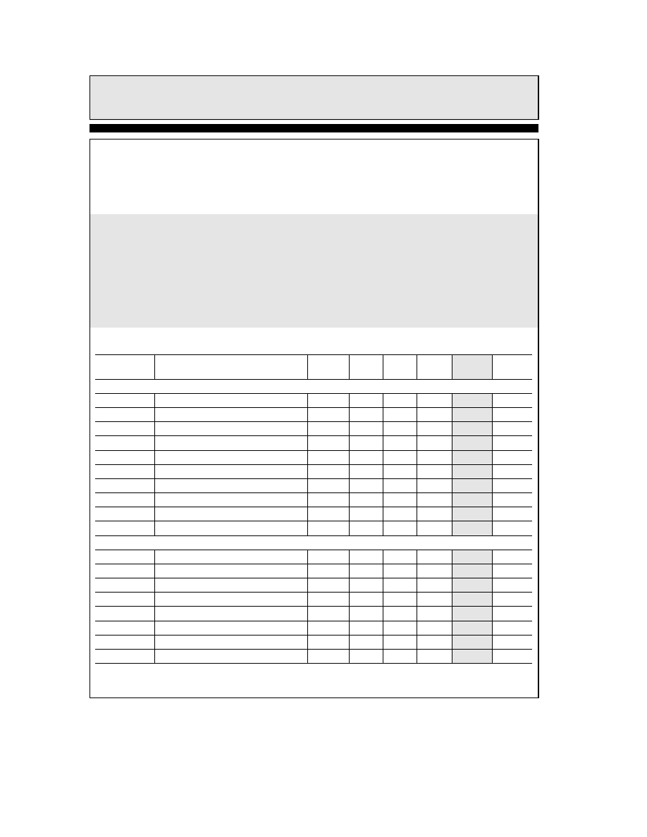
Open Loop DC Electrical Characteristics
Supplies at
g
15V Load
e
1K
X
Parameter
Description
Temp
Min
Typ
Max
Test
Units
Level
Amplifier Section (not restored)
V
OS
Input Offset Voltage
a
25 C
2
15
II
mV
I
B
a
I
IN
a
Input Bias Current
a
25 C
0 2
5
II
mA
I
B
b
I
IN
b
Input Bias Current
a
25 C
10
65
II
mA
R
OL
Transimpedance (Note 1)
a
25 C
100
220
II
k
X
R
IN
b
I
N
b
Resistance
a
25 C
50
V
X
CMRR
Common-Mode Rejection Ratio (Note 2)
a
25 C
50
56
II
dB
PSRR
Power Supply Rejection Ratio (Note 4)
a
25 C
50
70
II
dB
V
O
Output Voltage Swing R
L
e
1k
X
a
25 C
g
12
g
13
II
V
I
SC
Short-Circuit Current
a
25 C
45
70
100
II
mA
I
SY
Supply Current (Quiescent)
a
25 C
10
20
32
II
mA
Restoring Section
V
OS
COMP
Composite Input Offset Voltage (Note 3)
a
25 C
8
35
II
mV
I
B
a
R
Restore I
N
a
Input Bias Current
a
25 C
0 2
5
II
mA
I
OUT
Restoring Current Available
a
25 C
2
4
II
mA
PSRR
Power Supply Rejection Ratio (Note 4)
a
25 C
50
70
II
dB
G
OUT
Conductance
a
25 C
8
V
mA V
I
SY
RES
Supply Current Restoring
a
25 C
10
23
37
II
mA
V
IL
RES
RES Logic Low Threshold
a
25 C
1 0
1 4
II
V
V
IH
RES
RES Logic High Threshold
a
25 C
1 4
1 8
II
V
2
TD
is
41in
EL4390C
Triple 80 MHz Video Amplifier with DC Restore
Open Loop DC Electrical Characteristics
Supplies at
g
15V Load
e
1K
X
Contd
Parameter
Description
Temp
Min
Typ
Max
Test
Units
Level
Restoring Section
I
IL
RES
RES Input Current Logic Low
a
25 C
2
10
II
mA
I
IH
RES
RES Input Current Logic High
a
25 C
0 5
3
II
mA
Note 1 For current feedback amplifiers A
VOL
e
R
OL
R
IN
b
Note 2 V
CM
e
g
10V for V
S
e
g
15V
Note 3 Measured from V
CL
to amplifier output while restoring
Note 4 V
OS
is measured at V
S
e
g
4 5V and V
S
e
g
16V both supplies are changed simultaneously
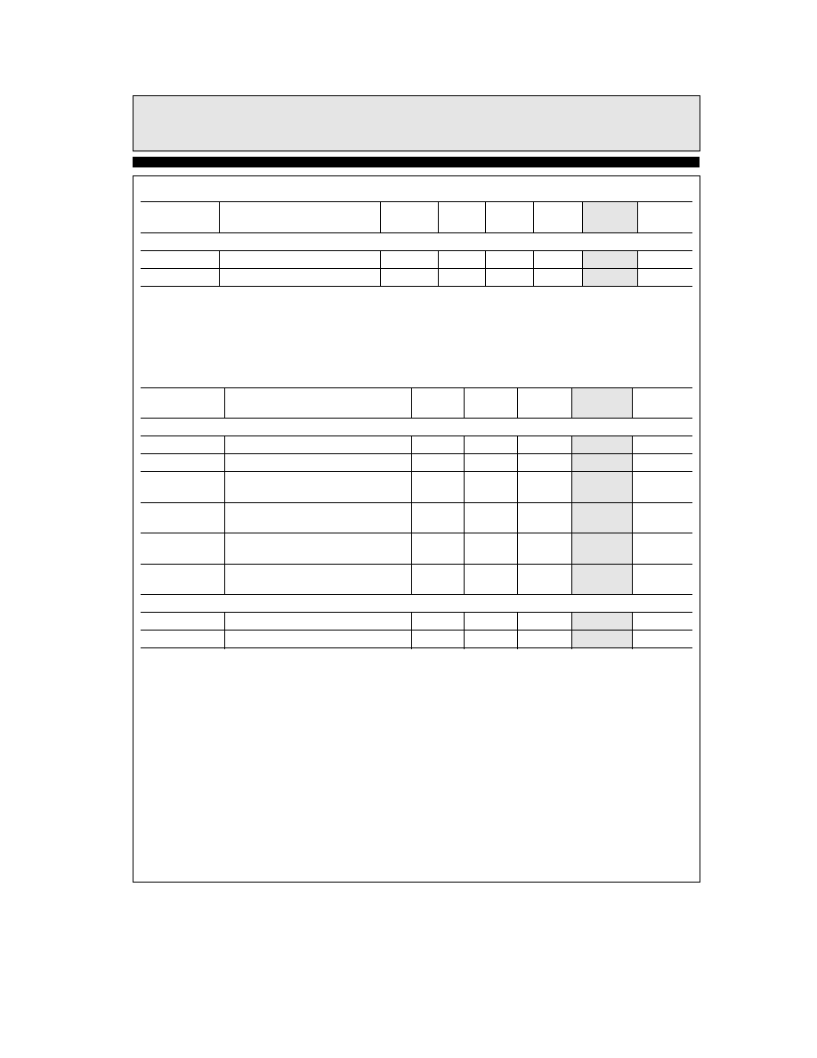
Closed Loop AC Electrical Characteristics
Supplies at
g
15V Load
e
150
X and 15 pF T
A
e
25 C (See note 7 re test fixture)
Parameter
Description
Min
Typ
Max
Test
Units
Level
Amplifier Section
SR
Slew Rate (Note 5)
800
V
V
ms
SR
Slew Rate w
g
5V Supplies (Note 5)
550
V
V
ms
BW
Bandwidth
b
3dB A
V
e
1
95
V
MHz
g
5V Supplies
b
3dB
72
V
MHz
BW
Bandwidth
b
0 1 dB
20
V
MHz
g
5V Supplies
b
0 1dB
14
V
MHz
dG
Differential Gain at 3 58 MHz
0 02
V
%
at
g
5V Supplies (Note 6)
0 02
V
%
d
i
Differential Phase at 3 58 MHz
0 03
V
( )
at
g
5V Supplies (Note 6)
0 06
V
( )
Restoring Section
T
RE
Time to Enable Restore
35
V
ns
T
RD
Time to Disable Restore
35
V
ns
Note 5 SR is measured at 20% to 80% of 4V pk-pk square wave with A
V
e
5 R
F
e
820
X R
G
e
200
X
Note 6 DC offset from
b
0 714V to
a
0 714V AC amplitude is 286m Vp-p equivalent to 40 ire
Note 7 Test fixture was designed to minimize capacitance at the I
N
b
input A ``good'' fixture should have less than 2 pF of stray
capacitance to ground at this very sensitive pin See application notes for further details
3
TD
is
09in
TD
is
27in

EL4390C
Triple 80 MHz Video Amplifier with DC Restore
Table 1 Charge Storage Capacitor Value vs Droop and Charging Rates
Cap Value
Droop in
Charge in
Charge in
(nF)
60mS (mV)
2mS (mV)
4mS (mV)
10
30
400
800
22
13 6
182
364
47
6 4
85
170
100
3 0
40
80
220
1 36
18
36
These numbers represent the worst case bias current and the worst case charging current Note that to
get the full (2mA
a
) charging current the clamp input must have
l
250mV of error voltage
Note that the magnitude of the bias current will decrease as temperature increases
The basic droop formula is
V (droop)
e
I
B
a
c
(Line time
b
Charge time)
capacitor value
and the basic charging formula is
V (charge)
e
I
OUT
c
Charge time
capacitor value
Where I
OUT
is
I
OUT
e
(Clamp voltage
b
IN
a
voltage)
120
4

EL4390C
Triple 80 MHz Video Amplifier with DC Restore
Typical Performance Curves
Gain Flatness
for Various R
F
V
S
e
g
15V A
V
e
0 dB
4390 ≠ 2
Gain Flatness
for Various R
F
V
S
e
g
5V A
V
e
0 dB
4390 ≠ 3
Gain Flatness
for Various R
F
and R
G
Values
V
S
e
g
15V A
V
e
6 dB
4390 ≠ 4
Gain Flatness
for Various R
F
and R
G
Values
V
S
e
g
5V A
V
e
6 dB
4390 ≠ 6
Phase Shift
for A
V
e
2
R
F
e
R
G
e
1300X
4390 ≠ 5
Phase Shift for A
V
e
2
R
F
e
R
G
e
1000X
at V
S
e
g
5V and V
S
e
g
15V
4390 ≠ 7
Gain Flatness
V
S
e
g
15V A
V
e
14 dB
R
F
R
G
as Shown
4390 ≠ 8
Gain Flatness
V
S
e
g
5V A
V
e
14 dB
R
F
R
G
as Shown
4390 ≠ 9
Phase Shift
for A
V
e
5 dB R
F
e
820X
R
G
e
200X V
S
e
g
5V
4390 ≠ 10
5