 | –≠–ª–µ–∫—Ç—Ä–æ–Ω–Ω—ã–π –∫–æ–º–ø–æ–Ω–µ–Ω—Ç: EL4422CS | –°–∫–∞—á–∞—Ç—å:  PDF PDF  ZIP ZIP |
EL4421C22C41C42C43C44C
January
1996
Rev
C
EL4421C 22C 41C 42C 43C 44C
Multiplexed-Input Video Amplifiers
Note All information contained in this data sheet has been carefully checked and is believed to be accurate as of the date of publication however this data sheet cannot be a ``controlled document'' Current revisions if any to these
specifications are maintained at the factory and are available upon your request We recommend checking the revision level before finalization of your design documentation
1994 Elantec Inc
Features
Unity or
a
2-gain bandwidth of
80 MHz
70 dB off-channel isolation at
4 MHz
Directly drives high-impedance
or 75
X loads
02% and 02 differential gain
and phase errors
8 ns switching time
k
100 mV switching glitch
0 2% loaded gain error
Compatible with
g
3V to
g
15V
supplies
160 mW maximum dissipation at
g
5V supplies
Ordering Information
Part No
Temp Range
Package
Outline
EL4421CN b40 C to a85 C 8-Pin PDIP MDP0031
EL4421CS b40 C to a85 C 8-Pin SO
MDP0027
EL4422CN b40 C to a85 C 8-Pin PDIP MDP0031
EL4422CS b40 C to a85 C 8-Pin SO
MDP0027
EL4441CN b40 C to a85 C 14-Pin PDIP MDP0031
EL4441CS b40 C to a85 C 14-Pin SO
MDP0027
EL4442CN b40 C to a85 C 14-Pin PDIP MDP0031
EL4442CS b40 C to a85 C 14-Pin SO
MDP0027
EL4443CN b40 C to a85 C 14-Pin PDIP MDP0031
EL4443CS b40 C to a85 C 14-Pin SO
MDP0027
EL4444CN b40 C to a85 C 14-Pin PDIP MDP0031
EL4444CS b40 C to a85 C 14-Pin SO
MDP0027
General Description
The EL44XX family of video multiplexed-amplifiers offers a
very quick 8 ns switching time and low glitch along with very
low video distortion The amplifiers have good gain accuracy
even when driving low-impedance loads To save power the am-
plifiers do not require heavy loading to remain stable
The EL4421 and EL4422 are two-input multiplexed amplifiers
The -inputs of the input stages are wired together and the de-
vice can be used as a pin-compatible upgrade from the
MAX453
The EL4441 and EL4442 have four inputs also with common
feedback These may be used as upgrades of the MAX454
The EL4443 and EL4444 are also 4-input multiplexed amplifi-
ers but both positive and negative inputs are wired separately
A wide variety of gain- and phase-switching circuits can be built
using independent feedback paths for each channel
The EL4421 EL4441 and EL4443 are internally compensated
for unity-gain operation The EL4422 EL4442 and EL4444 are
compensated for gains of
a
2 or more especially useful for driv-
ing back-matched cables
The amplifiers have an operational temperature of
b
40 C to
a
85 C and are packaged in plastic 8- and 14-pin DIP and 8- and
14-pin SO
The EL44XX multiplexed-amplifier family is fabricated with
Elantec's proprietary complementary bipolar process which
gives excellent signal symmetry and is very rugged
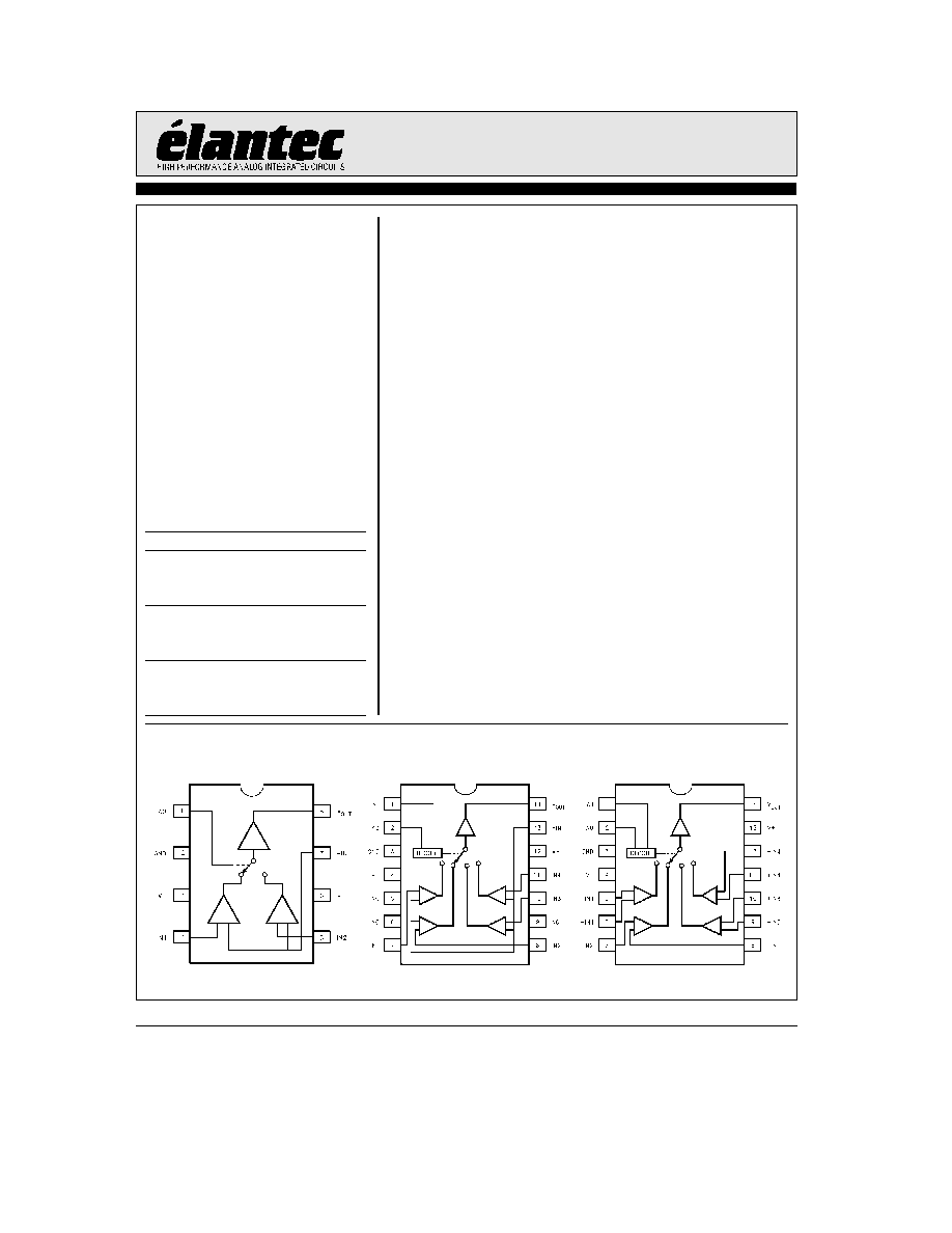
Connection Diagrams
EL4421 EL4422
4421 ≠ 1
EL4441 EL4442
4421 ≠ 2
EL4443 EL4444
4421 ≠ 3
Manufactured under U S Patent No 5 352 987
EL4421C 22C 41C 42C 43C 44C
Multiplexed-Input Video Amplifiers
Absolute Maximum Ratings
V
a
Positive Supply Voltage
16 5V
V
S
V
a
to V
b
Supply Voltage
33V
V
IN
Voltage at any Input or Feedback
V
a
to V
b
DV
IN
Difference between Pairs of
Inputs or Feedback
6V
V
LOGIC
Voltage at A0 or A1
b
4V to 6V
I
IN
Current into any Input
4 mA
Feedback or Logic Pin
I
OUT
Output Current
30 mA
P
D
Maximum Power Dissipation
See Curves
Important Note
All parameters having Min Max specifications are guaranteed The Test Level column indicates the specific device testing actually
performed during production and Quality inspection Elantec performs most electrical tests using modern high-speed automatic test
equipment specifically the LTX77 Series system Unless otherwise noted all tests are pulsed tests therefore T
J
e
T
C
e
T
A
Test Level
Test Procedure
I
100% production tested and QA sample tested per QA test plan QCX0002
II
100% production tested at T
A
e
25 C and QA sample tested at T
A
e
25 C
T
MAX
and T
MIN
per QA test plan QCX0002
III
QA sample tested per QA test plan QCX0002
IV
Parameter is guaranteed (but not tested) by Design and Characterization Data
V
Parameter is typical value at T
A
e
25 C for information purposes only
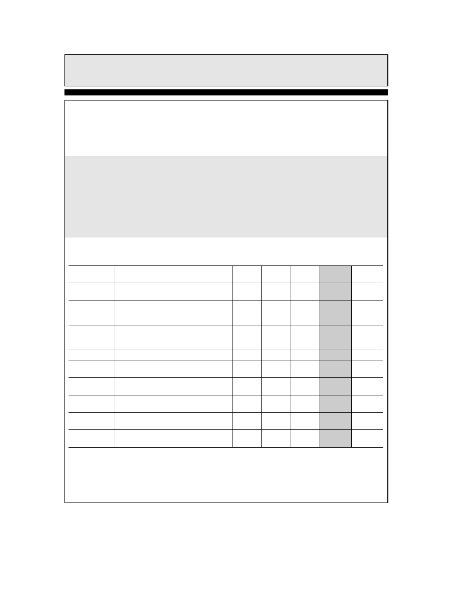
Open-Loop DC Electrical Characteristics
Power supplies at
g
5V T
A
e
25 C R
L
e
500
X unless otherwise specified
Parameter
Description
Min
Typ
Max
Test
Units
Level
V
OS
Input Offset Voltage
21 41 and 43
b
9
g
3
9
I
mV
22 42 and 44
b
7
g
2
7
I
I
B
Input Bias Current Positive Inputs Only
of the 21 22 41 42 and All Inputs of
b
12
b
5
0
I
mA
the 43 and 44
I
FB
Input Bias Currents of Common Feedback
b
21 and 22
b
24
b
10
0
I
mA
b
41 and 42
b
48
b
20
0
I
mA
I
OS
Input Offset Currents of the 43 and 44
60
350
I
nA
E
G
Gain Error of the 21 and 41 and 43
0 2
0 6
I
%
22 42 and 44
(Note 1)
0 1
0 6
I
V V
A
VOL
Open-Loop Gain
EL4443
350
500
I
V V
(Note 1)
EL4444
500
750
I
V V
V
IN
Input Signal Range EL4421 and EL4441
g
2 5
g
3
I
V
(Note 2)
CMRR
Common-Mode Rejection Ratio EL4443
70
90
I
dB
and EL4444
PSRR
Power Supply Rejection Ratio
60
70
I
dB
V
s
from
g
5V to
g
15V
2
TD
is
33in

EL4421C 22C 41C 42C 43C 44C
Multiplexed-Input Video Amplifiers
Open-Loop DC Electrical Characteristics
Contd
Power supplies at
g
5V T
A
e
25 C
Parameter
Description
Min
Typ
Max
Test
Units
Level
CMIR
Common-Mode Input Range
g
2 5
g
3
I
V
(Note 3) EL4443 and EL4444
V
OUT
Output Swing
g
2 5
g
3 5
I
V
I
SC
Output Short-Circuit Current
g
40
g
80
I
mA
F
T
Unselected Channel Feedthrough '21 '41 '43
70
80
I
dB
Attenuation (Note 1)
'22 '42 '44
55
64
I
dB
I
LOGIC
Input Current at A0 and A1
b
16
b
8
0
I
mA
with Input
e
0V and 5V
V
LOGIC
Logic Valid High and Low Input Levels
0 8
2 0
I
V
I
S
Supply Current
EL4421 and EL4422
11
14
I
mA
EL4441 EL4442 EL4443 and EL4444
13
16
Note 1 The 21
41 and 43 devices are connected for unity-gain operation with 75
X load and an input span of
g
1V The 22
42
and 44 devices are connected for a gain of
a
2 with a 150
X load and a
g
1V input span with R
F
e
R
G
e
270
X
Note 2 The 21 and 41 devices are connected for unity gain with a
g
3V input span while the output swing is measured
Note 3 CMIR is assured by passing the CMRR test at input voltage extremes
Closed-Loop AC Electrical Characteristics
Power supplies at
g
5V T
A
e
25 C for EL4421 EL4441 and EL4443 A
V
e a
1 and R
L
e
500
X for EL4422 EL4442 and EL4444
A
V
e a
2 and R
L
e
150
X with R
F
e
R
G
e
270
X and C
F
e
3 pF for all C
L
e
15 pF
Parameter
Description
Min
Typ
Max
Test
Units
Level
BW
b
3 dB
b
3 dB Small-Signal Bandwidth EL4421 '41 '43
80
V
MHz
EL4422 '42 '44
65
V
MHz
BW
g
0 1 dB
0 1 dB Flatness Bandwidth
10
V
MHz
Peaking
Frequency Response Peaking
0 5
V
dB
SR
Slewrate V
OUT
between
b
2 5V and
a
2 5V V
S
e
g
12V
EL4421 EL4441 EL4443
150
200
I
V
msec
EL4422 EL4442 EL4444
180
240
I
V
msec
V
n
Input-Referred Noise Voltage Density
EL4421 EL4441 EL4443
18
V
nV rt-hz
EL4422 EL4442 EL4444
14
V
nV rt-hz
d
G
Differential Gain Error V
OFFSET
between
b
0 7V and
a
0 7V
EL4421 EL4441 EL4443 (V
S
e
g
12V)
0 01
V
%
EL4421 EL4441 EL4443 (V
S
e
g
5V)
0 10
V
%
EL4422 EL4442 EL4444 (V
S
e
g
12V)
0 02
V
%
EL4422 EL4442 EL4444 (V
S
e
g
5V)
0 11
V
%
3
TD
is
22in
TD
is
26in
EL4421C 22C 41C 42C 43C 44C
Multiplexed-Input Video Amplifiers
Closed-Loop AC Electrical Characteristics
Power supplies at
g
5V T
A
e
25 C for EL4421 EL4441 and EL4443 A
V
e a
1 and R
L
e
500
X for EL4422 EL4442 and EL4444
A
V
e
a
2 and R
L
e
150
X with R
F
e
R
G
e
270
X and C
F
e
3 pF for all C
L
e
15 pF
Contd
Parameter
Description
Min
Typ
Max
Test
Units
Level
d
O
Differential Phase Error V
OFFSET
between
b
0 7V and
a
0 7V
EL4421 EL4441 EL4443 (V
S
e
g
12V)
0 01
V
EL4421 EL4441 EL4443 (V
S
e
g
5V)
0 1
V
EL4422 EL4442 EL4444 (V
S
e
g
12V)
0 02
V
EL4422 EL4442 EL4444 (V
S
e
g
5V)
0 15
V
T
MUX
Multiplex Delay Time Logic Threshold to 50% Signal Change
EL4421 '22
8
V
nsec
EL4441 '42 '43 '44
12
V
nsec
V
GLITCH
Peak Multiplex Glitch
EL4421 '22
70
V
mV
EL4441 '42 '43 '44
100
V
mV
ISO
Channel Off Isolation at 3 58 MHz (See Text)
EL4421 EL4441 EL4443
76
V
dB
EL4422 EL4442 EL4444
63
V
dB
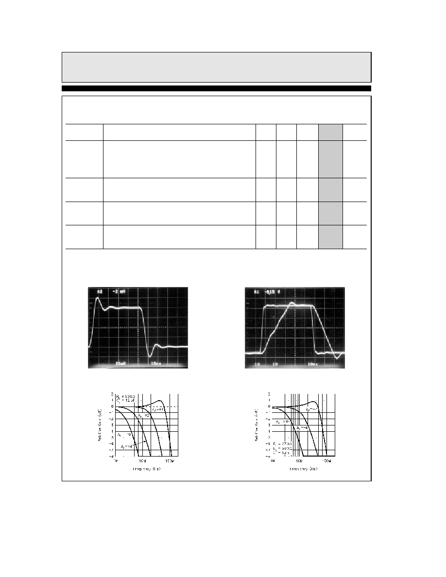
Typical Performance Curves
V
S
e
g
5V R
L
e
500X
Small-Signal Transient Response
EL4421 EL4441 and EL4443
4421 ≠ 5
V
S
e
g
12V R
L
e
500X
Large-Signal Response
EL4421 EL4441 and EL4443
4421 ≠ 6
Various Gains
Frequency Response for
EL4421 EL4441 and EL4443
4421 ≠ 7
Frequency Response for
EL4422 EL4442 and EL4444
Various Gains
4421 ≠ 8
4
TD
is
24in
EL4421C 22C 41C 42C 43C 44C
Multiplexed-Input Video Amplifiers
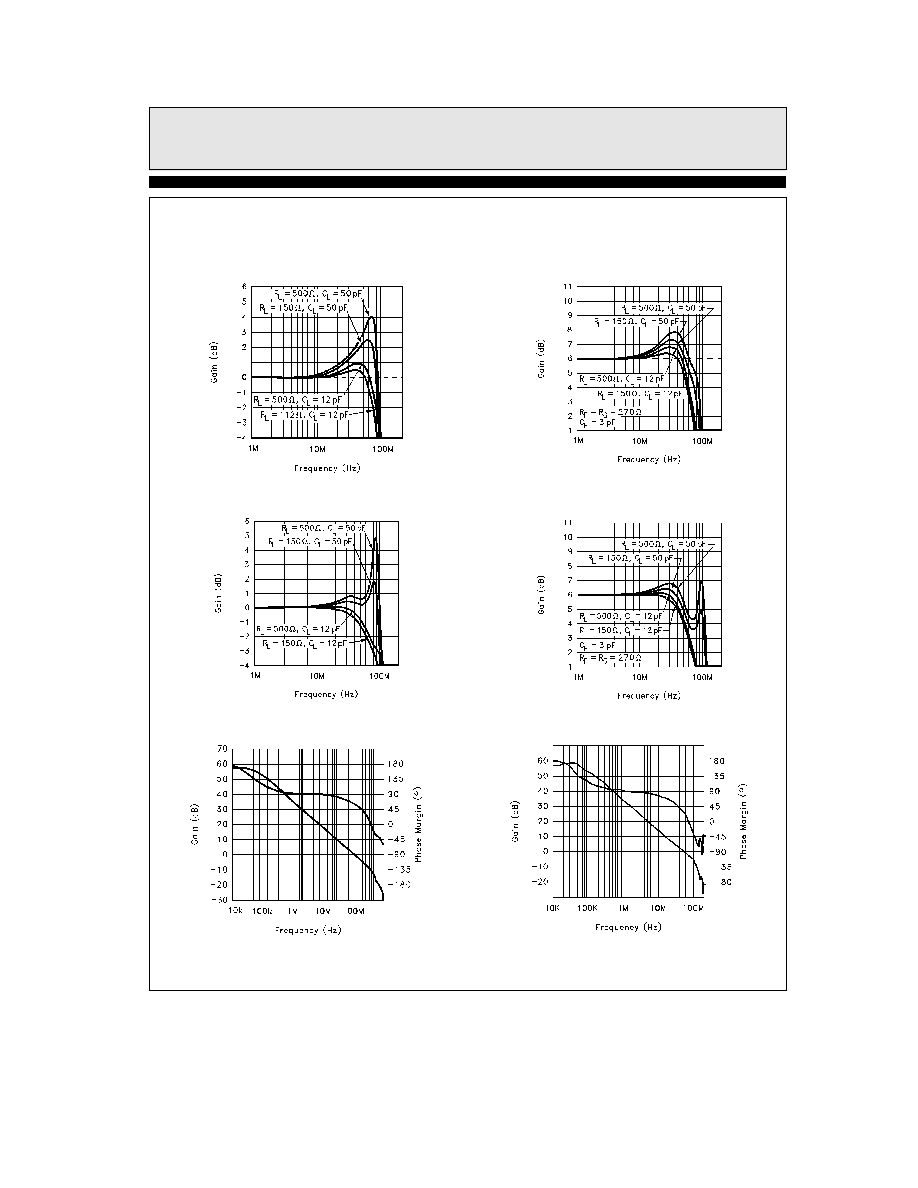
Typical Performance Curves
Contd
V
S
e
g
5V A
V
e
a
1
Frequency Response for Various Loads
EL4421 EL4441 and EL4443
4421 ≠ 9
V
S
e
g
5V A
V
e
a
2
Frequency Response for Various Loads
EL4422 EL4442 and EL4444
4421 ≠ 10
V
S
e
g
15V A
V
e
a
1
for Various Loads
Frequency Response
4421 ≠ 11
V
S
e
g
15V A
V
e
a
2
Frequency Response for Various Loads
EL4422 EL4442 and EL4444
4421 ≠ 12
Phase vs Frequency
EL4443 Open-Loop Gain and
4421 ≠ 13
Phase vs Frequency
EL4444 Open-Loop Gain and
4421 ≠ 37
5