 | –≠–ª–µ–∫—Ç—Ä–æ–Ω–Ω—ã–π –∫–æ–º–ø–æ–Ω–µ–Ω—Ç: EL4431CN | –°–∫–∞—á–∞—Ç—å:  PDF PDF  ZIP ZIP |

EL4430CEL4431C
January
1996
Rev
D
EL4430C EL4431C
Video Instrumentation Amplifiers
Note All information contained in this data sheet has been carefully checked and is believed to be accurate as of the date of publication however this data sheet cannot be a ``controlled document'' Current revisions if any to these
specifications are maintained at the factory and are available upon your request We recommend checking the revision level before finalization of your design documentation
1996 Elantec Inc
Features
Fully differential inputs and
feedback
Differential input range of
g
2V
Common-mode range of
g
12V
High CMRR at 4 MHz of
70 dB
Stable at gains of 1 2
Calibrated and clean input
clipping
4430
80 MHz
G
e
1
4431
160 MHz GBWP
380V ms slew rate
0 02% or differential gain or
phase
Operates on
g
5 to
g
15V
supplies with no AC degradation
Applications
Line receivers
``Loop-through'' interface
Level translation
Magnetic head pre-amplification
Differential-to-single-ended
conversion
Ordering Information
Part No
Temp Range
Package
Outline
EL4430CN
b
40 C to
a
85 C 8-pin P-DIP MDP0031
EL4430CS
b
40 C to
a
85 C 8-lead SO
MDP0027
EL4431CN
b
40 C to
a
85 C 8-pin P-DIP
MDP0031
EL4431CS
b
40 C to
a
85 C 8-lead SO
MDP0027
General Description
The EL4430 and 4431 are video instrumentation amplifiers
which are ideal for line receivers differential-to-single-ended
converters transducer interfacing and any situation where a
differential signal must be extracted from a background of com-
mon-mode noise or DC offset
These devices have two differential signal inputs and two differ-
ential feedback terminals The FB terminal connects to the am-
plifier output or a divided version of it to increase circuit gain
and the REF terminal is connected to the output ground or
offset reference
The EL4430 is compensated to be stable at a gain of 1 or more
and the EL4431 for a gain of 2 or more
The amplifiers have an operational temperature of
b
40 C to
a
85 C and are packaged in plastic 8-pin DIP and SO-8
The EL4430 and EL4431 are fabricated with Elantec's proprie-
tary complementary bipolar process which gives excellent sig-
nal symmetry and is free from latchup
Connection Diagram
4430 ≠ 1

EL4430C EL4431C
Video Instrumentation Amplifiers
Absolute Maximum Ratings
(T
A
e
25 C)
V
a
Positive Supply Voltage
16 5V
V
S
V
a
to V
b
Supply Voltage
33V
V
IN
Voltage at any Input or Feedback
V
a
to V
b
DV
IN
Difference between Pairs
of Inputs or Feedback
6V
I
IN
Current into any Input or Feedback Pin
4 mA
I
OUT
Continuous Output Current
30 mA
P
D
Maximum Power Dissipation
See Curves
T
A
Operating Temperature Range
b
40 C to
a
85 C
T
S
Storage Temperature Range
b
60 C to
a
150 C
Important Note
All parameters having Min Max specifications are guaranteed The Test Level column indicates the specific device testing actually
performed during production and Quality inspection Elantec performs most electrical tests using modern high-speed automatic test
equipment specifically the LTX77 Series system Unless otherwise noted all tests are pulsed tests therefore T
J
e
T
C
e
T
A
Test Level
Test Procedure
I
100% production tested and QA sample tested per QA test plan QCX0002
II
100% production tested at T
A
e
25 C and QA sample tested at T
A
e
25 C
T
MAX
and T
MIN
per QA test plan QCX0002
III
QA sample tested per QA test plan QCX0002
IV
Parameter is guaranteed (but not tested) by Design and Characterization Data
V
Parameter is typical value at T
A
e
25 C for information purposes only
Open-Loop DC Electrical Characteristics
Power supplies at
g
5V T
A
e
25
For the EL4431
R
F
e
R
G
e
500
X
Parameter
Description
Min
Typ
Max
Test
Units
Level
V
DIFF
Differential input voltage - Clipping
EL4430 31
2 0
2 3
I
V
(V
CM
e
0)
0 1% nonlinearity
EL4430 31
1 8
V
V
V
CM
Common-mode range (V
DIFF
e
0)
V
S
e
g
5V
g
2
g
3 0
I
V
V
S
e
g
15V
g
12
g
13 0
I
V
V
OS
Input offset voltage
EL4430 31
2
8
I
mV
I
B
Input bias current (IN
a
IN
b
REF and FB terminals)
12
20
I
mA
I
OS
Input offset current between IN
a
and IN
b
0 2
2
I
mA
and between REF and FB
R
IN
Input resistance
EL4430 31
100
230
I
k
X
CMRR
Common-mode rejection ratio
70
90
I
dB
PSRR
Power supply rejection ratio
EL4430 31
60
V
dB
E
G
Gain error excluding feedback resistors
EL4430 31
b
1 5
b
0 2
a
0 5
I
%
V
O
Output voltage swing
EL4430 V
S
e
g
5V
g
2
g
2 8
I
V
V
S
e
g
15V
g
12
g
12 8
I
V
EL4431 V
S
e
g
5V
g
2 5
g
3 0
I
V
V
S
e
g
15V
g
12 5
g
13 0
I
V
I
SC
Output short-circuit current
40
90
I
mA
I
S
Supply current V
S
e
g
15V
13 5
16
I
mA
2
TD
is
35in

EL4430C EL4431C
Video Instrumentation Amplifiers
Closed-Loop AC Electrical Characteristics
Power supplies at
g
12V T
A
e
25 C R
L
e
500
X for
the EL4430 R
L
e
150
X for the EL4431 C
L
e
15 pF For the EL4431 R
F
e
R
G
e
500
X
Parameter
Description
Min
Typ
Max
Test
Units
Level
BW
b
3 dB
b
3 dB small-signal bandwidth
EL4430
82
V
MHz
EL4431
80
V
MHz
BW
g
0 1 dB
0 1 dB flatness bandwidth
EL4430
20
V
MHz
EL4431
14
V
MHz
Peaking
Frequency response peaking
EL4430
0 6
V
dB
EL4431
1 0
V
dB
SR
Slew rate V
OUT
between
b
2V and
a
2V
All
380
V
V
ms
V
N
Input-referred noise voltage density
EL4430 31
26
V
nV rt-Hz
dG
Differential gain error Voffset between
EL4430
0 02
V
%
b
0 7V and
a
0 7V
EL4431 R
L
e
150
X
0 04
V
%
d
i
Differential gain error Voffset between
EL4430
0 02
V
( )
b
0 7V and
a
0 7V
EL4431 R
L
e
150
X
0 08
V
( )
T
S
Settling time to 0 1% from a 4V step
EL4430
48
V
ns
Test Circuit
4430 ≠ 3
Typical
Performance
Curves
EL4430 and EL4431
Common-Mode Rejection
Ratio vs Frequency
4430 ≠ 4
3
TD
is
25in

EL4430C EL4431C
Video Instrumentation Amplifiers
Typical Performance Curves
Contd
EL4430 Frequency Response
vs Gain
4430 ≠ 5
EL4430 Frequency Response
for Various R
L
C
L
V
S
e
g
5V
4430 ≠ 6
EL4430 Frequency Response
for Various R
L
C
L
V
S
e
g
15V
4430 ≠ 7
EL4431 Frequency Response
vs Gain
4430 ≠ 8
EL4431 Frequency Response
for Various R
L
C
L
V
S
e
g
5V
4430 ≠ 9
EL4431 Frequency Response
for Various R
L
C
L
V
S
e
g
15V
4430 ≠ 10
4
EL4430C EL4431C
Video Instrumentation Amplifiers
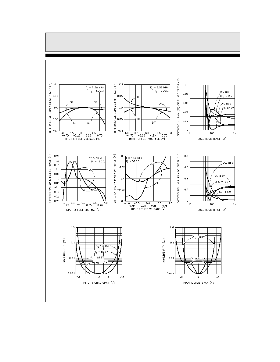
Typical Performance Curves
Contd
EL4430 Differential Gain
and Phase vs Input Offset
Voltage for V
S
e
g
5V
4430 ≠ 14
EL4430 Differential Gain
and Phase vs Input Offset
Voltage for V
S
e
g
12V
4430 ≠ 15
EL4430 Differential Gain
and Phase Error vs R
L
4430 ≠ 16
EL4431 Differential Gain
and Phase vs Input Offset
Voltage for V
S
e
g
5V
4430 ≠ 17
EL4431 Differential Gain
and Phase vs Input Offset
Voltage for V
S
e
g
12V
4430 ≠ 18
EL4431 Differential Gain
and Phase Error vs R
L
4430 ≠ 19
EL4430 Nonlinearity
vs Input Signal Span
4430 ≠ 20
EL4431 Nonlinearity
vs Input Signal Span
4430 ≠ 21
5