 | –≠–ª–µ–∫—Ç—Ä–æ–Ω–Ω—ã–π –∫–æ–º–ø–æ–Ω–µ–Ω—Ç: EL4453 | –°–∫–∞—á–∞—Ç—å:  PDF PDF  ZIP ZIP |

EL4453C
January
1995
Rev
A
EL4453C
Video Fader
Note All information contained in this data sheet has been carefully checked and is believed to be accurate as of the date of publication however this data sheet cannot be a ``controlled document'' Current revisions if any to these
specifications are maintained at the factory and are available upon your request We recommend checking the revision level before finalization of your design documentation
1995 Elantec Inc
Features
Complete two-input fader with
output amplifier
uses no extra
components
80 MHz bandwidth
Fast fade control speed
Operates on
g
5V to
g
15V
supplies
l
60 dB attenuation
5 MHz
Applications
Mixing two inputs
Picture-in-picture
Text overlay onto video
General gain control
Ordering Information
Part No
Temp Range
Pkg
Outline
EL4453CN
b
40 C to
a
85 C 14-Pin P-DIP
MDP0031
EL4453CS
b
40 C to
a
85 C 14-Lead SOIC MDP0027
General Description
The EL4453C is a complete fader subsystem It variably blends
two inputs together for such applications as video picture-in-
picture effects
The EL4453C operates on
g
5V to
g
15V supplies and has an
analog differential input range of
g
2V AC characteristics do
not change appreciably over the supply range
The circuit has an operational temperature of
b
40 C to
a
85 C
and is packaged in 14-pin P-DIP and SO-14
The EL4453C is fabricated with Elantec's proprietary comple-
mentary bipolar process which gives excellent signal symmetry
and is free from latch up
Connection Diagram
4453 ≠ 1
EL4453C
Video Fader
Absolute Maximum Ratings
T
A
e
25 C
V
a
Positive Supply Voltage
16 5V
V
S
V
a
to V
b
Supply Voltage
33V
V
IN
Voltage at any Input or Feedback
V
a
to V
b
DV
IN
Difference between Pairs
of Inputs or Feedback
6V
I
IN
Current into any Input or Feedback Pin
4 mA
I
OUT
Output Current
30 mA
P
D
Maximum Power Dissipation
See Curves
T
A
Operating Temperature Range
b
40 C to
a
85 C
T
S
Storage Temperature Range
b
60 C to
a
150 C
Important Note
All parameters having Min Max specifications are guaranteed The Test Level column indicates the specific device testing actually
performed during production and Quality inspection Elantec performs most electrical tests using modern high-speed automatic test
equipment specifically the LTX77 Series system Unless otherwise noted all tests are pulsed tests therefore T
J
e
T
C
e
T
A
Test Level
Test Procedure
I
100% production tested and QA sample tested per QA test plan QCX0002
II
100% production tested at T
A
e
25 C and QA sample tested at T
A
e
25 C
T
MAX
and T
MIN
per QA test plan QCX0002
III
QA sample tested per QA test plan QCX0002
IV
Parameter is guaranteed (but not tested) by Design and Characterization Data
V
Parameter is typical value at T
A
e
25 C for information purposes only
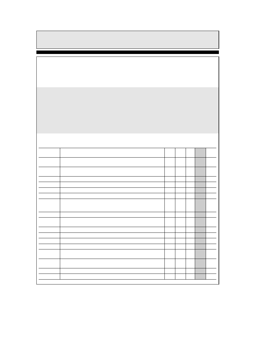
Open-Loop DC Electrical Characteristics
Power Supplies at
g
5V Sum
a e
Sum
b e
0 T
A
e
25 C
Parameter
Description
Min
Typ
Max
Test
Units
Level
V
DIFF
V
IN
A V
IN
B or Sum Differential Input Voltage
Clipping
1 8
2 0
I
V
0 2% Nonlinearity
0 7
V
V
V
CM
Common-Mode Range (All Inputs V
DIFF
e
0)
V
S
e
g
5V
g
2 5
g
2 8
I
V
V
S
e
g
15V
g
12 5
g
12 8
I
V
V
OS
A or B Input Offset Voltage
25
I
mV
V
FADE
100% Extrapolated Voltage for 100% Gain for V
IN
A
0 9
1 05
1 2
I
V
V
FADE
0%
Extrapolated Voltage for 0% Gain for V
IN
A
b
1 2
b
1 15
b
0 9
I
V
I
B
Input Bias Current (All Inputs) with all V
IN
e
0
9
20
I
mA
I
OS
Input Offset Current between V
IN
A
a
and V
IN
A
b
0 2
4
I
mA
V
IN
B
a
and V
IN
B
b
Fade
a
and Fade
b
and Sum
a
and Sum
b
F
T
V
IN
A Signal Feedthrough V
FADE
e b
1 5V
b
100
b
60
I
dB
NL
A or B Input Nonlinearity V
IN
between
a
1V and
b
1V
V
IN
A or V
IN
B
0 2
0 5
I
%
Sum Input
0 5
V
%
R
IN
Signal
Input Resistance A B or Sum Input
230
V
k
X
R
IN
Fade
Input Resistance Fade Input
120
V
k
X
CMRR
Common-Mode Rejection Ratio V
IN
A or V
IN
B
70
80
I
dB
PSRR
Power Supply Rejection Ratio
50
70
I
dB
E
G
Gain Error V
FADE
e
1 5V
V
IN
A or V
IN
B
b
2
a
2
I
%
Sum Input
b
4
a
4
I
%
V
O
Output Voltage Swing
V
S
e
g
5V
g
2 5
g
2 8
I
V
(V
IN
e
0 V
REF
Varied)
V
S
e
g
15V
g
12 5
g
12 8
I
V
I
SC
Output Short-Circuit Current
40
85
I
mA
I
S
Supply Current V
S
e
g
15V
17
21
I
mA
2
TD
is
43in

EL4453C
Video Fader
Closed-Loop AC Electrical Characteristics
Power supplies at
g
12V T
A
e
25 C R
L
e
500
X C
L
e
15 pF V
FADE
e
1 5V Sum
a e
Sum
b e
0
Parameter
Description
Min
Typ
Max
Test
Units
Level
BW
b
3 dB
b
3 dB Small-Signal Bandwidth V
IN
A or V
IN
B
80
V
MHz
BW
g
0 1 dB
0 1 dB Flatness Bandwidth V
IN
A or V
IN
B
9
V
MHz
Peaking
Frequency Response Peaking
1 0
V
dB
BW Fade
b
3 dB Small-Signal Bandwidth Fade Input
80
V
MHz
SR
Slew Rate V
OUT
between
b
2V and
a
2V
TBD
380
I
V
ms
V
N
Input-Referred Noise Voltage Density
160
V
nV Hz
F
T
Feedthrough of Faded-Out Channel F
e
3 58 MHz
b
63
V
dB
dG
Differential Gain Error V
OFFSET
from 0 to
g
0 714V Fade at 100%
V
IN
A or V
IN
B
0 05
V
%
Sum Input
0 35
V
%
d
i
Differential Phase Error V
OFFSET
from 0 to
g
0 71V Fade at 100%
V
IN
A or V
IN
B
0 05
V
( )
Sum Input
0 1
V
( )
Test Circuit
4453 ≠ 2
Note For typical performance curves Sum
a
e
Sum
b
e
0 R
F
e
0
X R
G
e
%
V
FADE
e
a
1 5V and C
L
e
15 pF unless
otherwise noted
3
TD
is
25in
EL4453C
Video Fader
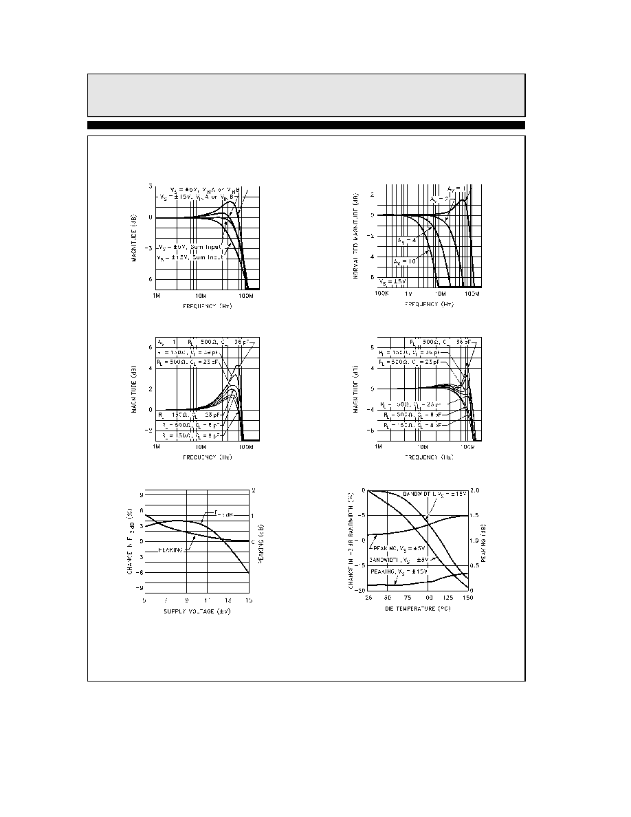
Typical Performance Curves
Frequency Response
4453 ≠ 3
Frequency Response vs Gain
4453 ≠ 4
Frequency Response for
Various Loads V
S
e
g
5V
4453 ≠ 6
Frequency Response for
Various Loads V
S
e
g
15V
4453 ≠ 7
b
3 dB Bandwidth and Peaking
vs Supply Voltage
4453 ≠ 9
b
3 dB Bandwidth and Peaking
vs Die Temperature
4453 ≠ 10
4
EL4453C
Video Fader
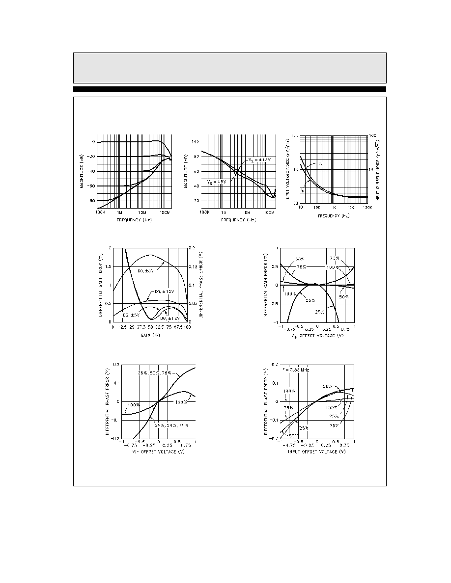
Typical Performance Curves
Contd
Frequency Response for
Different Gains V
S
e
g
5V
4453 ≠ 5
Input Common-Mode Rejection
Ratio vs Frequency
4453 ≠ 8
Input Voltage and Current
Noise vs Frequency
4453 ≠ 11
V
IN
Differential Gain
and Phase Error vs Gain
4453 ≠ 14
V
IN
Differential Gain Error
vs Input Offset Voltage
for Gain e 100% 75% 50% and 25%
4453 ≠ 15
V
IN
Differential Phase Error
vs Input Offset Voltage for Gain e
100% 75% 50% and 25% V
S
e
g
5V
4453 ≠ 16
V
IN
Differential Phase Error
vs Input Offset Voltage for Gain e
100% 75% 50% and 25% V
S
e
g
12V
4453 ≠ 17
5