© 2000 Elantec Semiconductor, Inc.
EL
4501C -
Preliminary
General Description
The EL4501C Video Front End (VFE) is an integrated solution that
provides the key analog signal conditioning functions for analog video
signals. It forms the front end interface for either an analog or ana-
log/digital video system. The VFE contains a high bandwidth DC
Restore, a sophisticated Sync Separator, and a Data Slicer for embed-
ded data recovery.
The VFE will perform the restoration of the DC reference level
(blanking level) and the extraction of all of the necessary timing sig-
nals needed for synchronization and control. The sync separator is
designed for very good noise immunity by incorporating a signal qual-
ification scheme and internal brick wall filter. A data slicer is also
included to help decode data embedded in the active video or VBI
areas of the signal.
The VFE operates from a single 5 volt supply and is available in a
small 24 pin QSOP package that takes only 0.08in
2
(54mm
2
)
of board
area, as well as a standard 24 pin SOIC.
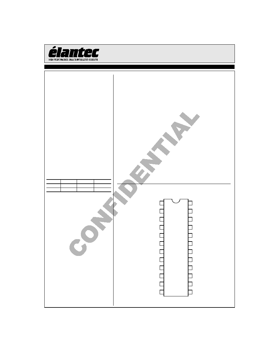
Connection Diagram
VIDEO_OUT
VFB
VIDEO_IN
DS_MODE
DS_ENAB
GND
GNDD
RFREQ
FSEL
SYNC_IN
LOS
COMPOSITE
HORIZONTAL
DS_OUT
DS_REF
REF_IN
REF_OUT
VS
VSD
SYNC_AMP
NC
BACK_PORCH
ODD/EVEN
VERTICAL
1
2
3
4
16
15
14
13
5
6
7
12
11
9
8
10
20
19
18
17
24
23
22
21
Features
∑ DC restore and sync separator
∑ Wideband (100MHz) DC restore
∑ Advanced sync separator
∑ Programmable data slicer
∑ Single 5 volt operation
∑ Differential Gain = 0.1%
∑ Differential Phase = 0.1∞
∑ Low power (<75mW)
Applications
∑ Video Capture & Editing
∑ Video Projectors
∑ Set Top Boxes
∑ Security Video
∑ Embedded data recovery
Ordering Information
Part No.
Temp. Range
Package
Outline #
EL4501CS
-40∞C to +85∞C
24-Pin SOIC
MDP0027
EL4501CU
-40∞C to +85∞C
24-Pin QSOP
MDP0031
EL4501C - Preliminary
Video Front End
Septe
m
ber 7, 2000
2
EL4501C - Preliminary
Video Front End
EL
4501C
-
Pre
l
iminary
Absolute Maximum Ratings
(T
A
= 25∞C)
Values beyond absolute maximum ratings can cause the device to be pre-
maturely damaged. Absolute maximum ratings are stress ratings only and
functional device operation is not implied.
Supply Voltage (V
S
to GND)
+6V
Input Voltage
GND - 0.3V, V
S
+0.3V
Storage Temperature Range
-65∞C to +150∞C
Ambient Operating Temperature
-40∞C to +85∞C
Operating Junction Temperature
125∞C
Power Dissipation
See Curves
Important Note:
All parameters having Min/Max specifications are guaranteed. Typ values are for information purposes only. Unless otherwise noted, all tests are at the
specified temperature and are pulsed tests, therefore: T
J
= T
C
= T
A
.
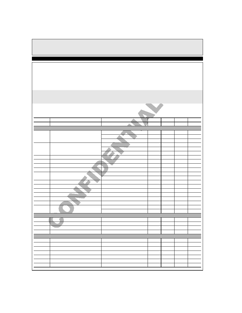
Electrical Characteristics
V
S
= +5V, GND = 0V, T
A
= 25∞C, Input Video = 1V
P-P
unless otherwise specified.
Parameter
Description
Conditions
Min
Typ
Max
Unit
I
S
Supply Current
No Load, V
IN
= 0V
20
mA
Video Amplifier Section
V
OP
Positive Output Voltage Swing
R
L
= 150
to V
S
/2
4.70
4.85
V
R
L
= 150
to GND
4.20
4.60
V
R
L
= 1k to V
S
/2
4.95
4.97
V
V
ON
Negative Output Voltage Swing
R
L
= 150
to V
S
/2
0.15
0.30
V
R
L
= 150
to GND
0
V
R
L
= 1k to V
S
/2
0.03
0.05
V
+I
OUT
Positive Output Current
RL = 10
to V
S
/2
60
80
120
mA
-I
OUT
Negative Output Current
RL = 10
to V
S
/2
-50
-60
-80
mA
dG
Differential Gain Error
[1]
Standard NTSC test, A
V
= 2, R
L
= 150
0.1
%
dP
Differential Phase Error
[1]
Standard NTSC test, A
V
= 2, R
L
= 150
0.1
∞
BW
Bandwidth
-3dB, G = 1, R
L
= 10k
to GND
100
MHz
-3dB, G = 1, R
L
= 150
to GND
60
MHz
BW1
Bandwidth
+/-0.1dB, G = 2, R
L
= 150
to GND
8
MHz
SR
Slew Rate
25% to 75%, 3.5V
P-P
, R
L
= 150
150
200
V/µs
V
RL
Ref Level Range
0
3.5
V
ts
Settling Time
to 0.1%, V
IN
= 0V to 3V
35
ns
R
IN
Input Resistance (VIDEO_IN)
90
115
140
k
C
IN
Input Capacitance (VIDEO_IN)
1.5
pF
A
VOL
Open Loop Voltage Gain
R
L
= no load, V
OUT
= 0.5V to 3V
54
65
dB
R
L
= 150
to GND, V
OUT
= 0.5V to 3V
40
50
dB
DC Restore Section
CMIR
Common Mode Input Range (REF_IN)
CMRR
TBD dB
0
3.5
V
V
OS
Input Offset Voltage
DC restored
-20
+20
mV
TCV
OS
Input Offset Voltage Temperature Coefficient
10
µV/∞C
I
B
Input Bias Current (REF_IN)
V
CM
= 0V to 3.5V
1
100
nA
Data Slicer Section
I
IH
Input High Current (DS_MODE & DS_ENAB)
V
IH
= 5V
4
6
µA
I
IL
Input Low Current (DS_MODE & DS_ENAB)
V
IL
= 0V
1
100
nA
V
IH
Input High Voltage (DS_MODE & DS_ENAB)
4.5
V
V
IL
Input Low Voltage (DS_MODE & DS_ENAB)
0.5
V
V
OH
Output High Voltage (DS_OUT)
I
OUT
= -1mA
4.75
4.9
V
V
OL
Output Low Voltage (DS_OUT)
I
OUT
= 1mA
0.1
0.25
V
I
OUT
Short Circuit Current (DS_OUT)
R
L
= 10
to 2.5V
15
20
mA

3
EL4501C - Preliminary
Video Front End
EL
4501C -
Preliminary
I
B
Input Bias Current (DS_REF)
DS_REF = 0V & 5V
-100
1
100
nA
Vos
Input Offset Voltage
-20
+20
mV
V
HYS
Hysteresis
10
15
mV
t
PD
Propagation Delay
50% to 50%
18
28
ns
t
R/F
Rise/Fall Time
10% to 90%, RL = 150k, CL = 5pF
1.2
1.8
ns
Sync Separator Section
V
OH
Output High Voltage
I
OH
= -1.6mA
4.6
V
V
OL
Output Low Voltage
I
OL
= 1.6mA
0.4
V
V
THSRH
Slicing Level
45
50
55
%
T
CD
Composite Sync Delay
With Filter
TBD
TBD
T
CD
Composite Sync Delay
Without Filter
TBD
TBD
V
SR
Sync In Reference Level
1.5
V
R
INSR
Sync Reference Input Impedance
90
k
V
RANGE
Input Dynamic Range
0.5
2.0
Vp-p
t
CD
Comp Sync Delay
From 50% point of leading edge of sync
50
75
100
ns
t
BD
Back Porch Delay
From 50% point of trailing edge of sync
340
430
520
ns
t
BW
Back Porch Width
2.7
3.0
3.3
µs
t
HD
Horiz Sync Delay
From 50% point of leading edge of sync
350
450
550
ns
t
HW
Horiz Sync Width
3.7
4.7
5.7
µs
t
VW
Vert Sync Width
Serrations
185
195
205
µs
t
VDD
Vert Sync Default Delay
No serrations
51
63.5
76
µs
f
H
Horiz Scan Rate
R
FREQ
= xx to yy k
15
130
kHz
V
LOS
LOS Detect Threshold
Compared to Sync Tip Amplitude
72
mV
t
JIT
Output Jitter
All sync separator outputs
5
ns
Reference Section
VREF
Reference Output Voltage (REF_OUT)
I
OUT
= +2mA to -0.5mA
1.2
1.3
1.4
V
Electrical Characteristics
V
S
= +5V, GND = 0V, T
A
= 25∞C, Input Video = 1V
P-P
unless otherwise specified.
Parameter
Description
Conditions
Min
Typ
Max
Unit

