 | –≠–ª–µ–∫—Ç—Ä–æ–Ω–Ω—ã–π –∫–æ–º–ø–æ–Ω–µ–Ω—Ç: EL4585C | –°–∫–∞—á–∞—Ç—å:  PDF PDF  ZIP ZIP |
EL4585C
March
1996
Rev
C
EL4585C
Horizontal Genlock 8 F
SC
Note All information contained in this data sheet has been carefully checked and is believed to be accurate as of the date of publication however this data sheet cannot be a ``controlled document'' Current revisions if any to these
specifications are maintained at the factory and are available upon your request We recommend checking the revision level before finalization of your design documentation
4585C
1995 Elantec Inc
Features
36 MHz general purpose PLL
8 F
SC
timing (Use the EL4584
for 4 F
SC
)
Compatible with EL4583C Sync
Separator
VCXO Xtal or LC tank
oscillator
k
2nS jitter (VCXO)
User-controlled PLL capture and
lock
Compatible with NTSC and PAL
TV formats
8 pre-programmed popular TV
scan rate clock divisors
Single 5V low current operation
Applications
Pixel Clock regeneration
Video compression engine
(MPEG) clock generator
Video Capture or digitization
PIP (Picture In Picture) timing
generator
Text or Graphics overlay timing
Ordering Information
Part No
Temp Range
Package
Outline
EL4585CN
b
40 C to
a
85 C 16-Pin DIP
MDP0031
EL4585CS
b
40 C to
a
85 C 16-Lead SO
MDP0027
For 3Fsc and 4Fsc clock frequency operation
see EL4584 datasheet
Demo Board
A demo PCB is available for this
product Request ``EL4584 5 Demo
Board''
General Description
The EL4585C is a PLL (Phase Lock Loop) sub system designed
for video applications but also suitable for general purpose use
up to 36 MHz In a video application this device generates a
TTL CMOS compatible Pixel Clock (Clk Out) which is a multi-
ple of the TV Horizontal scan rate and phase locked to it
The reference signal is a horizontal sync signal TTL CMOS
format which can be easily derived from an analog composite
video signal with the EL4583 Sync Separator An input signal
to ``coast'' is provided for applications where periodic distur-
bances are present in the reference video timing such as VTR
head switching The Lock detector output indicates correct lock
The divider ratio is four ratios for NTSC and four similar ratios
for the PAL video timing standards by external selection of
three control pins These four ratios have been selected for com-
mon video applications including 8 F
SC
6 F
SC
27 MHz (CCIR
601 format) and square picture elements used in some worksta-
tion graphics To generate 4 F
SC
3 F
SC
13 5 MHz (CCIR 601
format) etc use the EL4584 which does not have the addition-
al divide by 2 stage of the EL4585
For applications where these frequencies are inappropriate or
for general purpose PLL applications the internal divider can be
by passed and an external divider chain used
FREQUENCIES and DIVISORS
Function
6Fsc
CCIR 601
Square
8Fsc
Divisor
1702
1728
1888
2270
PAL Fosc (MHz)
26 602
27 0
29 5
35 468
Divisor
1364
1716
1560
1820
NTSC Fosc (MHz)
21 476
27 0
24 546
28 636
CCIR 601 divisors yield 1440 pixels in the active portion of each line for NTSC and PAL
Square pixels format gives 640 pixels for NTSC and 768 pixels for PAL
6Fsc frequencies do not yield integer divisors
Divisor does not include
d
2 block
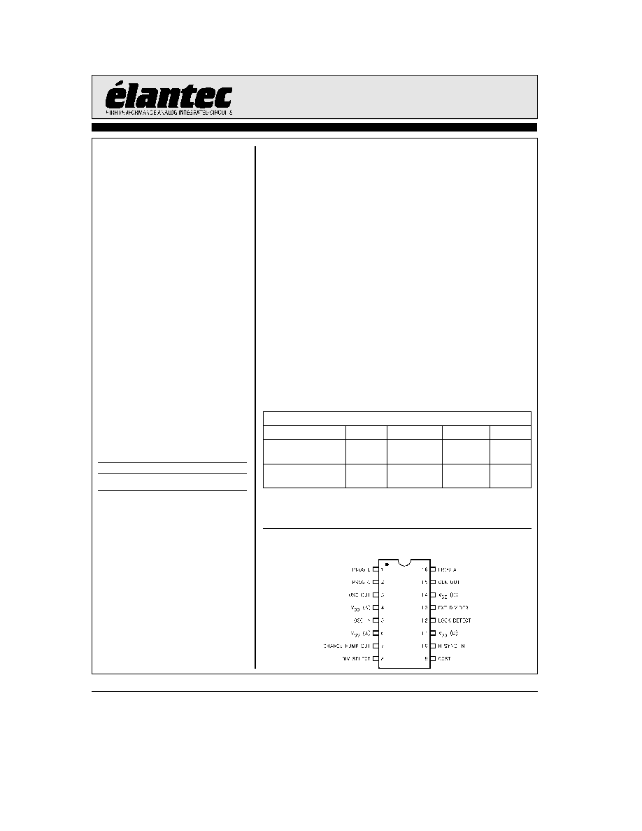
Connection Diagram
EL4585 SO P-DIP Packages
4585 ≠ 17
EL4585C
Horizontal Genlock 8 F
SC
Absolute Maximum Ratings
(T
A
e
25 C)
V
CC
Supply
7V
Storage Temperature
b
65 C to
a
150 C
Lead Temperature
260 C
Pin Voltages
b
0 5V to V
CC
a
0 5V
Operating Ambient Temperature Range
b
40 C to
a
85 C
Operating Junction Temp
125 C
Power Dissipation
400mW
Oscillator Frequency
36MHz
Important Note
All parameters having Min Max specifications are guaranteed The Test Level column indicates the specific device testing actually
performed during production and Quality inspection Elantec performs most electrical tests using modern high-speed automatic test
equipment specifically the LTX77 Series system Unless otherwise noted all tests are pulsed tests therefore T
J
e
T
C
e
T
A
Test Level
Test Procedure
I
100% production tested and QA sample tested per QA test plan QCX0002
II
100% production tested at T
A
e
25 C and QA sample tested at T
A
e
25 C
T
MAX
and T
MIN
per QA test plan QCX0002
III
QA sample tested per QA test plan QCX0002
IV
Parameter is guaranteed (but not tested) by Design and Characterization Data
V
Parameter is typical value at T
A
e
25 C for information purposes only
DC Electrical Characteristics
(V
DD
e
5V T
A
e
25 C unless otherwise noted)
Parameter
Conditions
Temp
Min
Typ
Max
Test
Units
Level
I
DD
V
DD
e
5V (Note 1)
25 C
2
4
I
mA
V
IL
Input Low Voltage
25 C
1 5
I
V
V
IH
Input High Voltage
25 C
3 5
I
V
I
IL
Input Low Current
All inputs except COAST V
in
e
1 5V
25 C
b
100
I
nA
I
IH
Input High Current
All inputs except COAST V
in
e
3 5V
25 C
100
I
nA
I
IL
Input Low Current
COAST pin V
in
e
1 5V
25 C
b
100
b
60
I
mA
I
IH
Input High Current
COAST pin V
in
e
3 5V
25 C
60
100
I
mA
V
OL
Output Low Voltage
Lock Det I
OL
e
1 6mA
25 C
0 4
I
V
V
OH
Output High Voltage
Lock Det I
OH
e b
1 6mA
25 C
2 4
I
V
V
OL
Output Low Voltage
CLK I
OL
e
3 2mA
25 C
0 4
I
V
V
OH
Output High Voltage
CLK I
OH
e b
3 2mA
25 C
2 4
I
V
V
OL
Output Low Voltage
OSC Out I
OL
e
200
mA
25 C
0 4
I
V
V
OH
Output High Voltage
OSC Out I
OH
e b
200
mA
25 C
2 4
I
V
I
OL
Output Low Current
Filter Out V
OUT
e
2 5V
25 C
200
300
I
mA
I
OH
Output High Current
Filter Out V
OUT
e
2 5V
25 C
b
300
b
200
I
mA
I
OL
I
OH
Current Ratio
Filter Out V
OUT
e
2 5V
25 C
1 05
1 0
0 95
I
I
LEAK
Filter Out
Coast Mode V
DD
l
V
OUT
l
0V
25 C
b
100
g
1
100
I
nA
Note 1 All inputs to 0V COAST floating
2
TD
is
35in
EL4585C
Horizontal Genlock 8 F
SC
AC Electrical Characteristics
(V
DD
e
5V T
A
e
25 C unless otherwise noted)
Parameter
Conditions
Temp
Min
Typ
Max
Test
Units
Level
VCO Gain
20 MHz
Test circuit 1
25 C
15 5
V
dB
H-sync S N Ratio
V
DD
e
5V (Note 2)
25 C
35
V
dB
Jitter
VCXO Oscillator
25 C
1
V
ns
Jitter
LC Oscillator (Typ)
25 C
10
V
ns
Note 2 Noisy video signal input to EL4583C H-sync input to EL4585C Test for positive signal lock
Pin Description
Pin No
Pin Name
Function
16 1 2
Prog A B C
Digital inputs to select
d
N value for internal counter See table below for values
3
Osc VCO Out
Output of internal inverter oscillator Connect to external crystal or LC tank VCO circuit
4
V
DD
(A)
Analog positive supply for oscillator PLL circuits
5
Osc VCO In
Input from external VCO
6
V
SS
(A)
Analog ground for oscillator PLL circuits
7
Charge Pump
Connect to loop filter If the H-sync phase is leading or H-sync frequency
l
CLK
d
2N current is
pumped into the filter capacitor to increase VCO frequency If H-sync phase is lagging or frequency
Out
k
CLK
d
2N current is pumped out of the filter capacitor to decrease VCO frequency During coast
mode or when locked charge pump goes to a high impedance state
8
Div Select
Divide select input When high the internal divider is enabled and EXT DIV becomes a test pin
outputting CLK
d
2N When low the internal divider is disabled and EXT DIV is an input from an
external
d
N
9
Coast
Tri-state logic input Low(
k
V
CC
)
e
normal mode Hi Z(or
to
V
CC
)
e
fast lock mode
High(
l
V
CC
)
e
coast mode
10
H-sync In
Horizontal sync pulse (CMOS level) input
11
V
DD
(D)
Positive supply for digital I O circuits
12
Lock Det
Lock Detect output Low level when PLL is locked Pulses high when out of lock
13
Ext Div
External Divide input when DIV SEL is low internal
d
2N output when DIV SEL is high
14
V
SS
(D)
Ground for digital I O circuits
15
CLK Out
Buffered output of the VCO
Table 5 VCO Divisors
Prog A
Prog B
Prog C
Div Value
Pin 16
Pin 1
Pin 2
N
0
0
0
1702
0
0
1
1728
0
1
0
1888
0
1
1
2270
1
0
0
1364
1
0
1
1716
1
1
0
1560
1
1
1
1820
3
TD
is
35in
TD
is
35in
EL4585C
Horizontal Genlock 8 F
SC
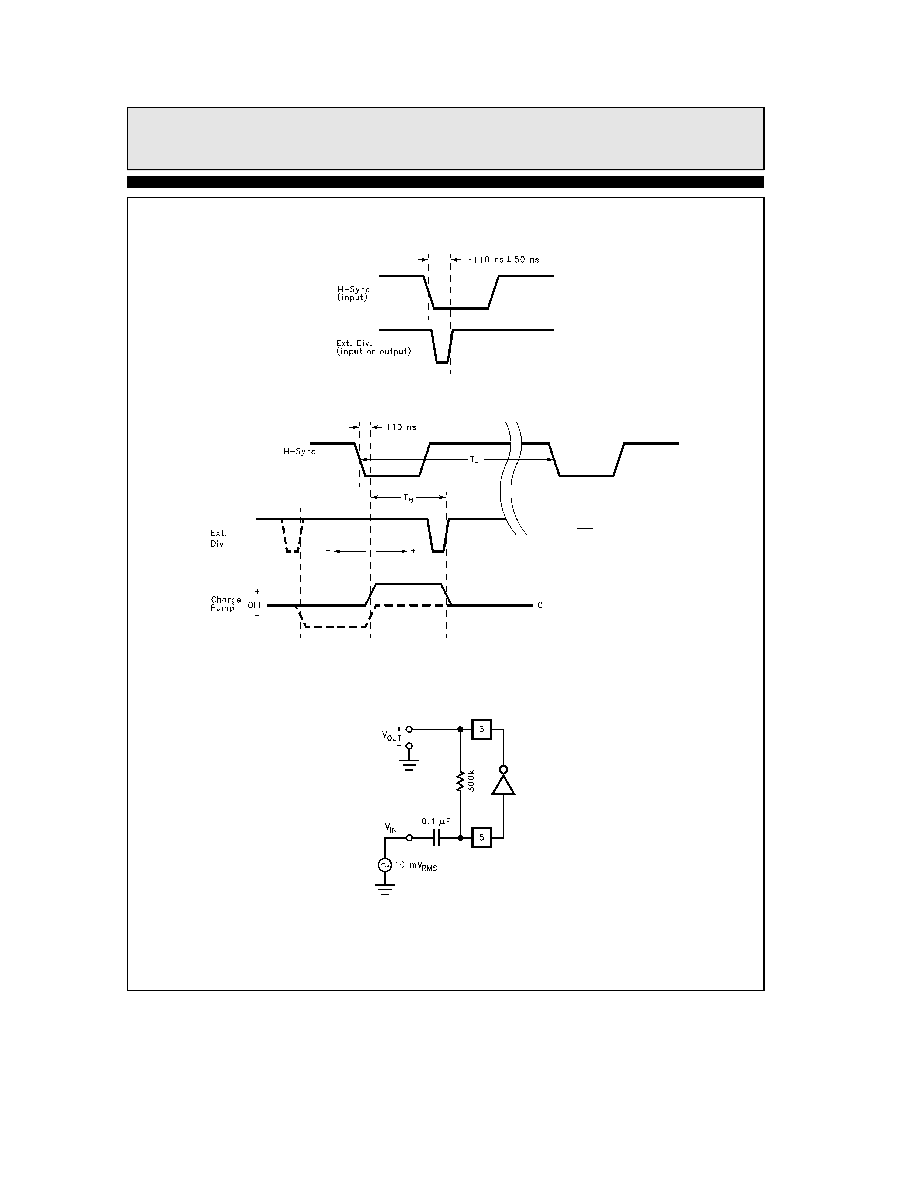
Timing Diagrams
PLL Locked Condition (Phase Error e 0)
4585 ≠ 2
Out of Lock Condition
i
E
e
T
i
T
H
c
360
T
H
e
H-sync period
T
i
e
phase error period
4585 ≠ 3
Typical Performance Curves
Test Circuit 1
4585 ≠ 5
4
EL4585C
Horizontal Genlock 8 F
SC
Typical Performance Curves
Contd
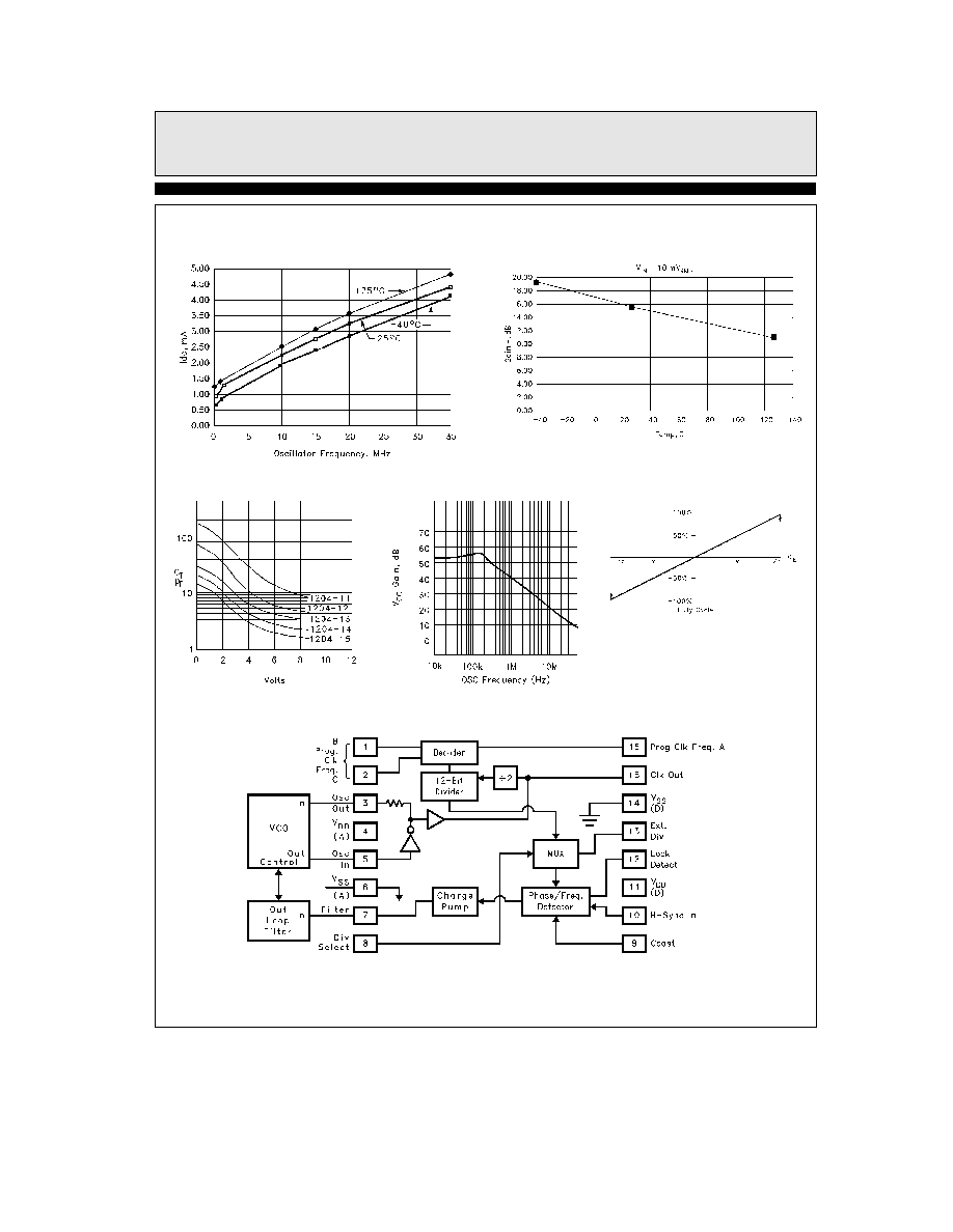
Idd vs Fosc
4585 ≠ 4
OSC Gain
20 MHz vs Temp
4585 ≠ 6
Typical Varactor
4585 ≠ 7
OSC Gain vs Fosc
4585 ≠ 8
Charge Pump Duty Cycle Vs i
E
4585 ≠ 9
EL4585 Block Diagram
4585 ≠ 1
5