Äîêóìåíòàöèÿ è îïèñàíèÿ www.docs.chipfind.ru
Note: All information contained in this data sheet has been carefully checked and is believed to be accurate as of the date of publication; however, this data sheet cannot be a "controlled document". Current revisions, if any, to these
specifications are maintained at the factory and are available upon your request. We recommend checking the revision level before finalization of your design documentation.
© 2001 Elantec Semiconductor, Inc.
E
L
5
1
8
5
C
-
P
r
e
l
i
m
i
n
a
r
y
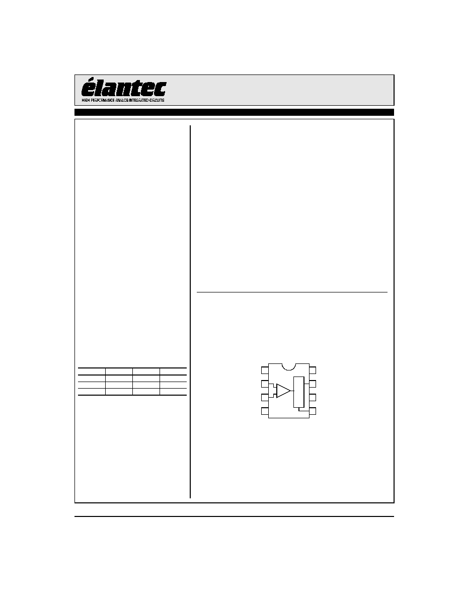
General Description
The EL5185C comparator is designed for operation in single supply
and dual supply applications with 5V to 12V between V
S
+ and V
S
-.
For single supplies, the inputs can operate from 0.1V below ground for
use in ground-sensing applications.
The output side of the comparator can be supplied from a single sup-
ply of 2.7V to 5V. The rail-to-rail output swing enables direct
connection of the comparator to both CMOS and TTL logic circuits.
The latch input of the EL5185C can be used to hold the comparator
output value by applying a low logic level to the pin.
The EL5185C is available in the 8-pin SO package and is specified for
operation over the -40°C to +85°C temperature range. Also available
are dual (EL5285C), window comparator (EL5287C), and quad
(EL5485C and EL5486C) versions.
Pin Configuration
1
2
3
4
8
7
6
5
VS+
L
A
T
C
H
VSD
OUT
GND
LATCH
IN+
IN-
VS-
EL5185CS
(8-Pin SO)
-
+
Features
· 4ns typ. propagation delay
· 5V to 12V input supply
· +2.7V to +5V output supply
· True-to-ground input
· Rail-to-rail outputs
· Separate analog and digital
supplies
· Active low latch
· Dual available (EL5285C)
· Window comparator (EL5287C)
· Quad available (EL5485C &
EL5486C)
· Pin-compatible 6ns family
available (EL5x81C, EL5283C &
EL5482C)
Applications
· Threshold detection
· High speed sampling circuits
· High speed triggers
· Line receivers
· PWM circuits
· High speed V/F converters
Ordering Information
Part No.
Package
Tape & Reel
Outline #
EL5185CS
8-Pin SO
-
MDP0027
EL5185CS-T7
8-Pin SO
7"
MDP0027
EL5185CS-T13
8-Pin SO
13"
MDP0027
EL5185C - Preliminary
4ns High-Speed Comparator
S
e
p
t
e
m
b
e
r
6
,
2
0
0
1
2
EL5185C - Preliminary
4ns High-Speed Comparator
E
L
5
1
8
5
C
-
P
r
e
l
i
m
i
n
a
r
y
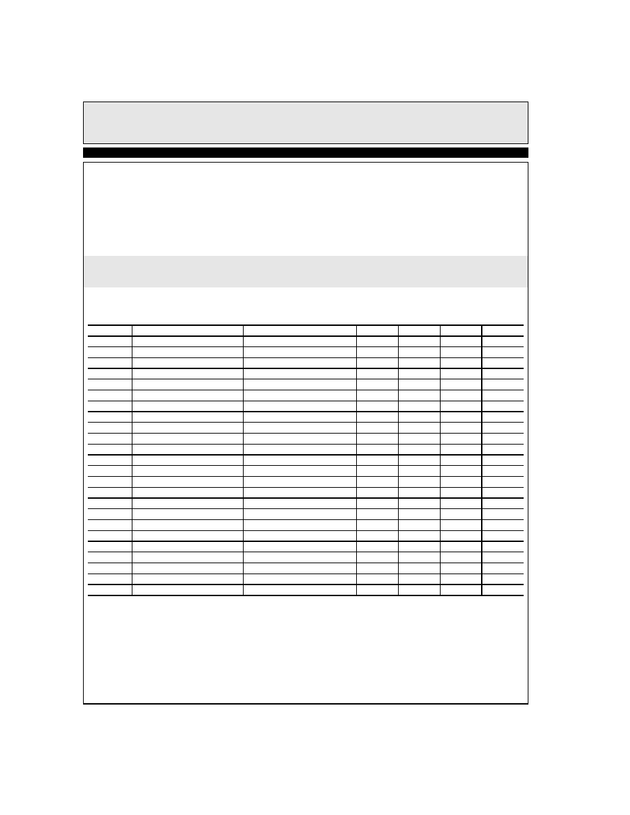
Absolute Maximum Ratings
(T
A
= 25°C)
Absolute maximum ratings are those values beyond which the device
could be permanently damaged. Absolute maximum ratings are stress
ratings only and functional device operation is not implied.
Analog Supply Voltage (V
S
+ to V
S
-)
+12.6V
Digital Supply Voltage (V
SD
to GND)
+7V
Differential Input Voltage
[(V
S
-) -0.2V] to [(V
S
+) +0.2V]
Common-mode Input Voltage
[(V
S
-) -0.2V] to [(V
S
+) +0.2V]
Latch Input Voltage
-0.2V to [V
SD
+0.2V]
Storage Temperature Range
-65°C to +150°C
Ambient operating Temperature
-40°C to +85°C
Operating Junction Temperature
+125°C
Power Dissipation
TBDmW
ESD Voltage
2kV
Important Note:
All parameters having Min/Max specifications are guaranteed. Typ values are for information purposes only. Unless otherwise noted, all tests are at the
specified temperature and are pulsed tests, therefore: T
J
= T
C
= T
A
.
Electrical Characteristics
V
S
= ±5V, V
SD
= 5V, R
L
= 2.3k
, C
L
= 15pF, T
A
= 25°C, unless otherwise specified.
Parameter
Description
Condition
Min
Typ
Max
Unit
V
OS
Input Offset Voltage
V
CM
= 0V, V
O
= 2.5V
2
4
mV
I
B
Input Bias Current
8
15
µA
C
IN
Input Capacitance
5
pF
I
OS
Input Offset Current
V
CM
= 0V, V
O
= 2.5V
100
500
nA
V
CM
Input Voltage Range
(V
S
-) - 0.1
(V
S
+) - 2V
V
A
VO
Large Signal Voltage Gain
5000
V/V
CMRR
Common-mode Rejection Ratio
-5V < V
CM
< +2.75V, V
O
= 2.5V
80
dB
PSRR
Power Supply Rejection Ratio
60
dB
V
OH
Output High Voltage
V
IN
> 250mV
V
SD
- 0.5V
V
SD
- 0.4V
V
V
OL
Output Low Voltage
V
IN
> 250mV
GND + 0.4V GND + 0.5V
V
V
LH
Latch Input Voltage High
2.0
V
V
LL
Latch Input Voltage Low
0.8
V
I
LH
Latch Input Current High
V
LH
= 3.0V
1
20
µA
I
LL
Latch Input Current Low
V
LL
= 0.3V
40
80
µA
I
S
+
Positive Analog Supply Current
10.5
mA
I
S
-
Negative Analog Supply Current
7.5
mA
I
DD
Digital Supply Current
6
mA
t
d
+
Positive Going Delay Time
V
OD
= 5mV, C
L
= 15pF, I
O
= 2mA
4
6
ns
t
d
-
Negative Going Delay Time
V
OD
= 5mV, C
L
= 15pF, I
O
= 2mA
4
6
ns
t
pd
+
Latch Disable to High Delay
6
ns
t
pd
-
Latch Disable to Low Delay
8
ns
t
s
Minimum Setup Time
2
ns
t
h
Minimum Hold Time
1
ns
t
pw
(D)
Minimum Latch Disable Pulse Width
5
ns
3
EL5185C - Preliminary
4ns High-Speed Comparator
E
L
5
1
8
5
C
-
P
r
e
l
i
m
i
n
a
r
y
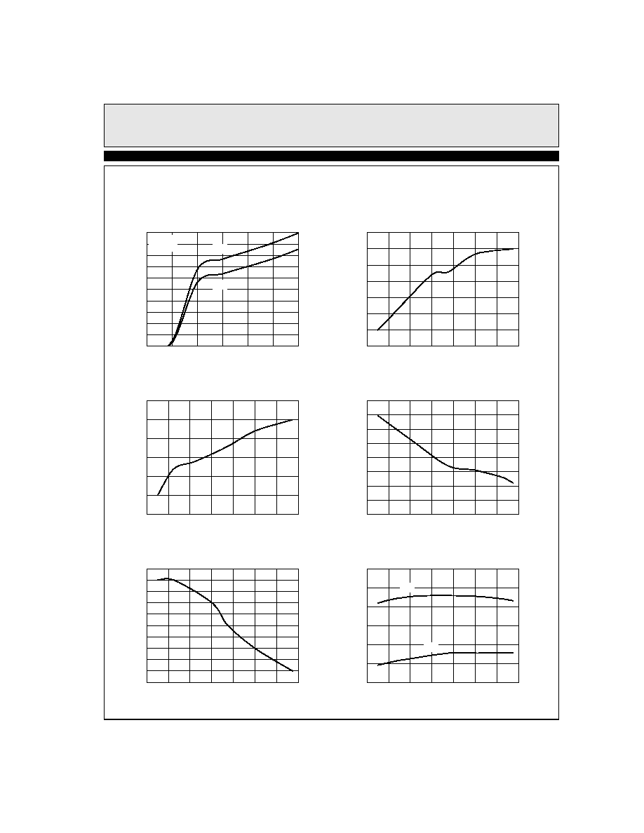
Typical Performance Curves
Supply Current vs Supply Voltage
(per comparator)
0
1
2
3
4
5
6
10
8
6
4
2
0
±V
S
(V)
I
S
(
m
A
)
I
S
+
I
S
-
V
IN
=50mV
R
L
=2.2k
Offset Voltage vs Temperature
-50
-30
10
30
50
70
90
3
2.5
1.5
1
0.5
0
Temperature (°C)
V
O
S
(
m
V
)
2
-10
Output Low Voltage vs Temperature
-50
-30
10
30
50
70
90
0.285
0.235
Temperature (°C)
V
O
L
(
V
)
-10
0.275
0.255
0.245
0.265
Output High Voltage vs Temperature
-50
-30
10
30
50
70
90
4.832
4.83
4.826
4.822
4.82
4.818
Temperature (°C)
V
O
H
(
V
)
4.828
4.824
-10
Input Bias Current vs Temperature
-50
-30
30
50
90
8
7
3
2
1
0
Temperature (°C)
I
B
(
µ
A
)
5
-10
Supply Current vs Temperature
(per comparator)
-50
10
70
90
12
11
8
6
Temperature (°C)
S
u
p
p
l
y
C
u
r
r
e
n
t
(
m
A
)
-30
7
50
10
70
6
4
10
9
30
-10
I
S
+
I
S
-
4
EL5185C - Preliminary
4ns High-Speed Comparator
E
L
5
1
8
5
C
-
P
r
e
l
i
m
i
n
a
r
y
Typical Performance Curves
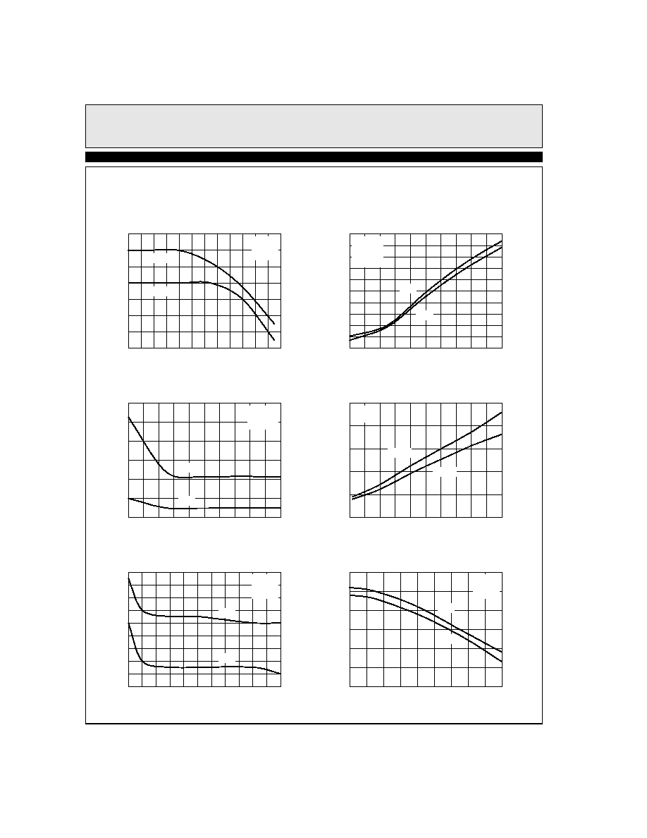
Propagation Delay vs Overdrive
V
IN
=5V
STEP
0.2
0.6
1
1.4
1.8
2.2
2.6
7.8
7.4
7
6.8
6.6
6.4
V
OD
(V)
D
e
l
a
y
T
i
m
e
(
n
s
)
Propagation Delay vs Supply Voltage
4
4.2
4.8
5.2
5.4
5.6
6
6.8
6.6
6.2
6
5.8
5.6
±V
S
(V)
D
e
l
a
y
T
i
m
e
(
n
s
)
6.4
4.4
Propagation Delay vs Source Resistance
V
IN
=1V
STEP
0
1.6
2
15
5
Source Resistance (k
)
D
e
l
a
y
T
i
m
e
(
n
s
)
13
Digital Supply Current vs Switching Frequency
(per comparator)
0
20
40
50
25
20
10
0
Frequency (MHz)
I
S
D
(
m
A
)
15
10
5
30
7.6
7.2
T
PD
-
T
PD
+
V
S
=±5V
V
SD
=5V
R
L
=2.2k
T
PD
-
T
PD
+
V
SD
=V
S
+
V
OD
=50mV
R
L
=2.2k
5
4.6
5.8
0.4
1.2
0.8
11
7
9
V
S
=±5V
V
SD
=5V
V
OD
=50mV
R
L
=2.2k
T
PD
-
T
PD
+
V
S
=±5V
T
A
=25°C
V
SD
=5V
V
SD
=3V
Propagation Delay vs Overdrive
V
IN
=1V
STEP
50 100
250 300
400
500
600
6.1
6
5.8
5.5
5.2
V
OD
(mV)
D
e
l
a
y
T
i
m
e
(
n
s
)
5.9
5.7
150
5.6
5.4
5.3
350
450
550
200
T
PD
-
T
PD
+
V
S
=±5V
V
SD
=5V
R
L
=2.2k
Propagation Delay vs Overdrive
V
IN
=3V
STEP
0.2
0.6
0.8
1.2
1.6
2
8
6.5
5
V
OD
(mV)
D
e
l
a
y
T
i
m
e
(
n
s
)
7.5
7
6
5.5
1
1.4
1.8
0.4
T
PD
-
T
PD
+
V
S
=±5V
V
SD
=5V
R
L
=2.2k
5
EL5185C - Preliminary
4ns High-Speed Comparator
E
L
5
1
8
5
C
-
P
r
e
l
i
m
i
n
a
r
y
Typical Performance Curves
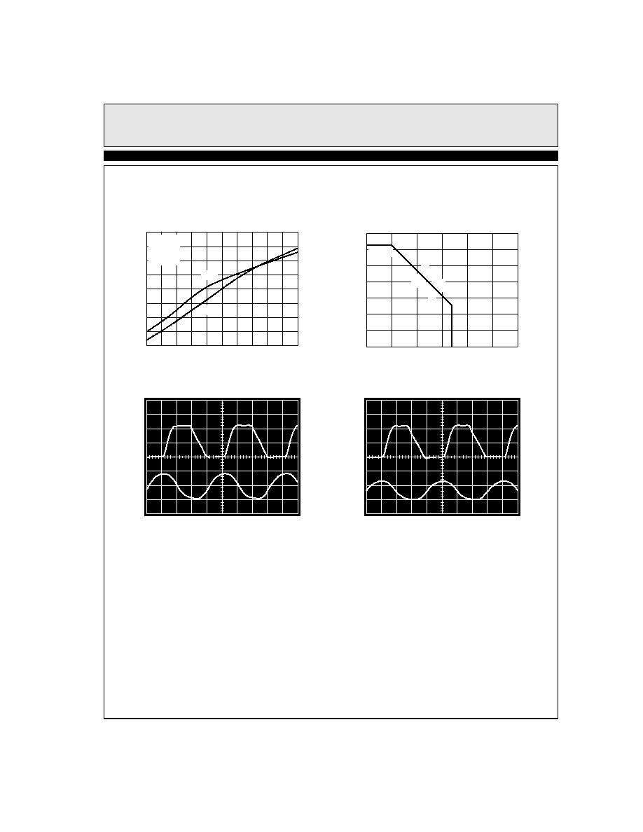
Output with 50MHz Input
V
IN
=1V
P-P
Output with 50MHz Input
V
IN
=3V
P-P
Output
(5ns/div,
2V/div)
Input
(5ns/div,
0.5V/div)
Output
(5ns/div,
2V/div)
Input
(5ns/div,
2V/div)
Propagation Delay vs Load Capacitance
V
IN
=1V
STEP
0
10
30
40
50
80
100
9
5
C
LOAD
(pF)
D
e
l
a
y
T
i
m
e
(
n
s
)
20
8.5
6.5
5.5
7.5
8
6
7
60
90
70
V
S
=±5V
V
SD
=5V
V
OD
=50mV
R
L
=2.2k
T
PD
-
T
PD
+
Package Power Dissipation vs Ambient Temp.
JEDEC JESD51-3 Low Effective Thermal Conductivity Test Board
0.7
0
0.5
0.3
0.2
0.1
P
o
w
e
r
D
i
s
s
i
p
a
t
i
o
n
(
W
)
0.6
0.4
0
125
100
75
50
25
Ambient Temperature (°C)
150
85
625mW
160
°C/W
SO
8