 | –≠–ª–µ–∫—Ç—Ä–æ–Ω–Ω—ã–π –∫–æ–º–ø–æ–Ω–µ–Ω—Ç: EL5197ACS | –°–∫–∞—á–∞—Ç—å:  PDF PDF  ZIP ZIP |
Note: All information contained in this data sheet has been carefully checked and is believed to be accurate as of the date of publication; however, this data sheet cannot be a "controlled document". Current revisions, if any, to these
specifications are maintained at the factory and are available upon your request. We recommend checking the revision level before finalization of your design documentation.
© 2002 Elantec Semiconductor, Inc.
E
L
5197C,
E
L
5197AC
General Description
The EL5197C and EL5197AC are fixed gain amplifiers with a band-
width of 200MHz, making these amplifiers ideal for today's high
speed video and monitor applications. These amplifiers feature inter-
nal gain setting resistors and can be configured in a gain of +1, -1 or
+2. The same bandwidth is seen in both gain-of-1 and gain-of-2
applications.
With a supply current of just 4mA and the ability to run from a single
supply voltage from 5V to 10V, these amplifiers are also ideal for
hand held, portable or battery powered equipment.
The EL5197AC also incorporates an enable and disable function to
reduce the supply current to 100µA typical per amplifier. Allowing the
CE pin to float or applying a low logic level will enable the amplifier.
The EL5197C is offered in the 5-pin SOT23 package and the
EL5197AC is available in the 6-pin SOT23 as well as the industry-
standard 8-pin SO packages. Both operate over the industrial tempera-
ture range of -40∞C to +85∞C.
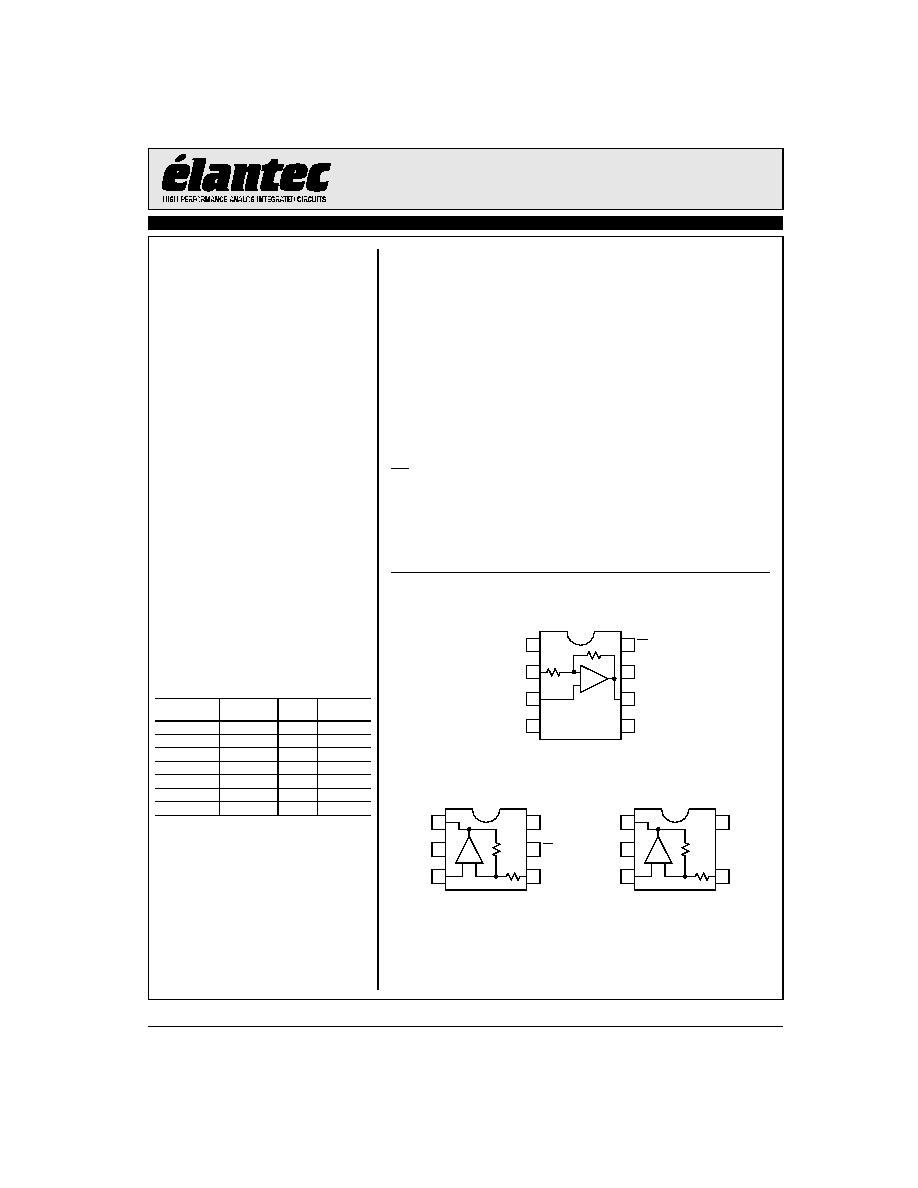
Pin Configurations
1
2
3
4
8
7
6
5
EL5197ACS
(8-Pin SO)
1
2
3
5
4
EL5197CW
(5-Pin SOT23)
1
2
3
6
4
EL5197ACW
(6-Pin SOT23)
-
+
-
+
NC
IN-
IN+
VS-
CE
VS+
OUT
NC
OUT
VS-
IN+
VS+
IN-
-
+
OUT
VS-
IN+
VS+
IN-
5 CE
Features
∑ Gain selectable (+1, -1, +2)
∑ 200MHz -3dB BW (A
V
= 1, 2)
∑ 4mA supply current
∑ Fast enable/disable (EL5197AC
only)
∑ Single and dual supply operation,
from 5V to 10V
∑ Available in SOT23 packages
∑ Triple (EL5397C) available
∑ 400MHz, 9mA product available
(EL5196C, EL5396C)
Applications
∑ Battery powered equipment
∑ Hand held, portable devices
∑ Video amplifiers
∑ Cable drivers
∑ RGB amplifiers
∑ Test equipment
∑ Instrumentation
∑ Current to voltage converters
Ordering Information
Part No
Package
Tape &
Reel
Outline #
EL5197CW-T7
5-Pin SOT23
7"
MDP0038
EL5197CW-T13
5-Pin SOT23
13"
MDP0038
EL5197ACW-T7
6-Pin SOT23
7"
MDP0038
EL5197ACW-T13
6-Pin SOT23
13"
MDP0038
EL5197ACS
8-Pin SO
-
MDP0027
EL5197ACS-T7
8-Pin SO
7"
MDP0027
EL5197ACS-T13
8-Pin SO
13"
MDP0027
EL5197C, EL5197AC
Single 200MHz Fixed Gain Amplifier with Enable
F
e
b
r
u
a
r
y
11,
2002
2
EL5197C, EL5197AC
Single 200MHz Fixed Gain Amplifier with Enable
E
L
5197C,
E
L
5197AC
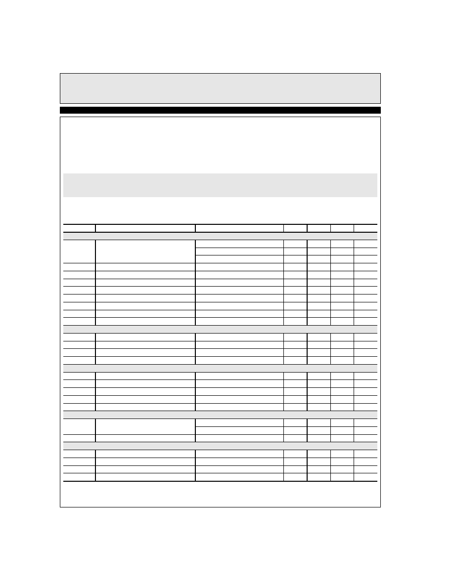
Absolute Maximum Ratings
(T
A
= 25∞C)
Values beyond absolute maximum ratings can cause the device to be pre-
maturely damaged. Absolute maximum ratings are stress ratings only and
functional device operation is not implied.
Supply Voltage between V
S
+ and V
S
-
11V
Maximum Continuous Output Current
50mA
Operating Junction Temperature
125∞C
Power Dissipation
See Curves
Pin Voltages
V
S
- - 0.5V to V
S
+ +0.5V
Storage Temperature
-65∞C to +150∞C
Operating Temperature
-40∞C to +85∞C
Important Note:
All parameters having Min/Max specifications are guaranteed. Typ values are for information purposes only. Unless otherwise noted, all tests are at the
specified temperature and are pulsed tests, therefore: T
J
= T
C
= T
A
.
Electrical Characteristics
V
S
+ = +5V, V
S
- = -5V, R
L
= 150
, T
A
= 25∞C unless otherwise specified.
Parameter
Description
Conditions
Min
Typ
Max
Unit
AC Performance
BW
-3dB Bandwidth
A
V
= +1
200
MHz
A
V
= -1
200
MHz
A
V
= +2
200
MHz
BW1
0.1dB Bandwidth
20
MHz
SR
Slew Rate
V
O
= -2.5V to +2.5V, A
V
= +2
1800
2200
V/µ s
t
S
0.1% Settling Time
V
OUT
= -2.5V to +2.5V, A
V
= -1
12
ns
e
N
Input Voltage Noise
4.4
nV/
Hz
i
N
-
IN- Input Current Noise
17
pA/
Hz
i
N
+
IN+ Input Current Noise
50
pA/
Hz
dG
Differential Gain Error
[1]
A
V
= +2
0.03
%
dP
Differential Phase Error
[1]
A
V
= +2
0.04
∞
DC Performance
V
OS
Offset Voltage
-10
1
10
mV
T
C
V
OS
Input Offset Voltage Temperature Coefficient
Measured from T
MIN
to T
MAX
5
µ V/∞C
A
E
Gain Error
V
O
= -3V to +3V
-2
1.3
2
%
R
F
, R
G
Internal R
F
and R
G
320
400
480
Input Characteristics
CMIR
Common Mode Input Range
±3V
±3.3V
V
+I
IN
+ Input Current
-60
1
60
µ A
-I
IN
- Input Current
-30
1
30
µ A
R
IN
Input Resistance
at I
N
+
45
k
C
IN
Input Capacitance
0.5
pF
Output Characteristics
V
O
Output Voltage Swing
R
L
= 150
to GND
±3.4V
±3.7V
V
R
L
= 1k
to GND
±3.8V
±4.0V
V
I
OUT
Output Current
R
L
= 10
to GND
95
120
mA
Supply
I
SON
Supply Current - Enabled
No load, V
IN
= 0V
3
4
5
mA
I
SOFF
Supply Current - Disabled
No load, V
IN
= 0V
100
150
µ A
PSRR
Power Supply Rejection Ratio
DC, V
S
= ±4.75V to ±5.25V
55
75
dB
-IPSR
- Input Current Power Supply Rejection
DC, V
S
= ±4.75V to ±5.25V
-2
2
µA/V
3
EL5197C, EL5197AC
Single 200MHz Fixed Gain Amplifier with Enable
E
L
5197C,
E
L
5197AC
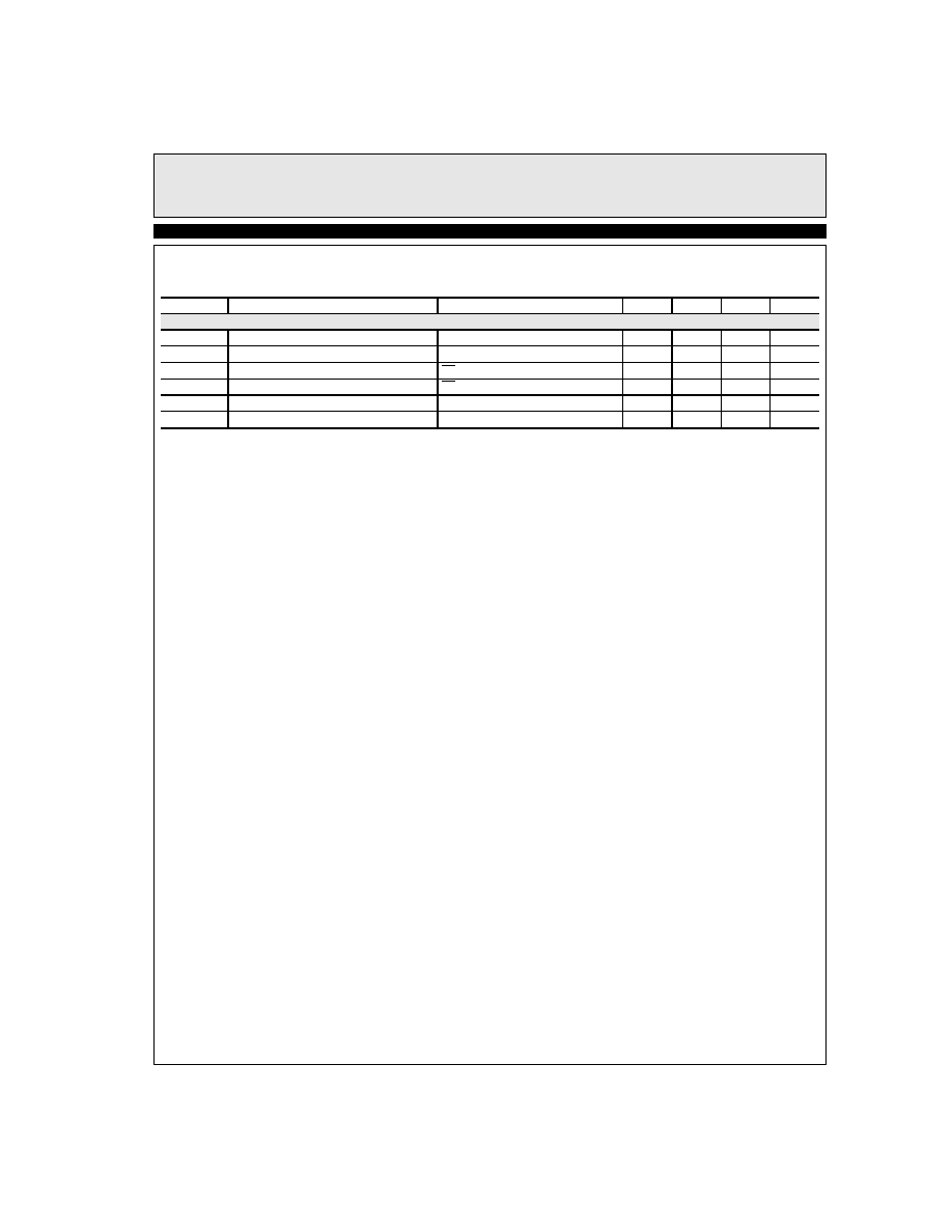
Enable (EL5197AC only)
t
EN
Enable Time
40
ns
t
DIS
Disable Time
600
ns
I
IHCE
CE Pin Input High Current
CE = V
S
+
0.8
6
µ A
I
ILCE
CE Pin Input Low Current
CE = V
S
-
0
-0.1
µ A
V
IHCE
CE Input High Voltage for Power-down
V
S
+ - 1
V
V
ILCE
CE Input Low Voltage for Power-down
V
S
+ - 3
V
1. Standard NTSC test, AC signal amplitude = 286mV
P-P
, f = 3.58MHz
Electrical Characteristics
V
S
+ = +5V, V
S
- = -5V, R
L
= 150
, T
A
= 25∞C unless otherwise specified.
Parameter
Description
Conditions
Min
Typ
Max
Unit

4
EL5197C, EL5197AC
Single 200MHz Fixed Gain Amplifier with Enable
E
L
5197C,
E
L
5197AC
Typical Performance Curves
Frequency Response (Gain)
1M
10M
100M
1G
6
2
-2
-6
-14
Frequency (Hz)
N
o
r
m
al
i
z
ed
M
a
g
n
i
t
u
d
e
(
d
B
)
A
V
=2
A
V
=1
A
V
=-1
R
L
=150
Frequency Response (Phase), All Gains
1M
10M
100M
1G
Frequency (Hz)
P
h
ase (
∞
)
R
L
=150
90
0
-90
-180
-270
-360
-10
Frequency Response for Various C
L
1M
10M
100M
1G
14
10
6
2
-6
Frequency (Hz)
N
o
r
m
al
i
z
ed
M
a
g
n
i
t
u
d
e (
d
B
)
A
V
=2
R
L
=150
22pF added
10pF added
0pF added
Group Delay vs Frequency
1M
10M
100M
1G
3.5
3
2
1
0
Frequency (Hz)
D
e
l
ay (
n
s)
A
V
=2
A
V
=1
R
L
=150
Frequency Response for Various Common-Mode Input
Voltages
1M
10M
100M
1G
6
-2
-6
-10
-14
Frequency (Hz)
N
o
r
m
al
i
z
ed
M
a
g
n
i
t
u
d
e
(
d
B
)
A
V
=2
R
L
=150
3V
0V
-3V
2.5
1.5
0.5
-2
2
Transimpedance (ROL) vs Frequency
1k
Frequency (Hz)
10k
100k
1M
10M
100M
1G
10M
100
1k
10k
100k
1M
Ma
g
n
i
t
ud
e
(
)
-90
-180
-270
-360
0
P
h
ase (
∞
)
Phase
Gain
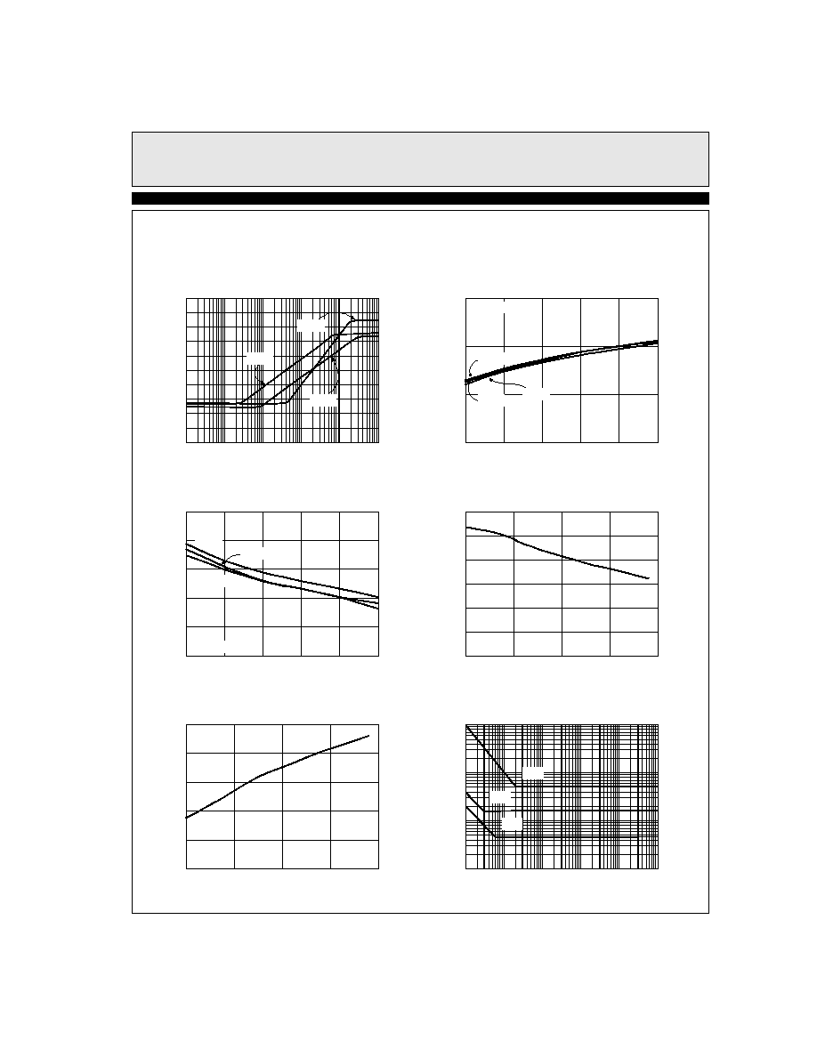
5
EL5197C, EL5197AC
Single 200MHz Fixed Gain Amplifier with Enable
E
L
5197C,
E
L
5197AC
Typical Performance Curves
PSRR and CMRR vs Frequency
P
S
RR
/
C
M
R
R (
d
B
)
Frequency (Hz)
20
-80
-60
-40
-20
0
10k
100k
1M
10M
1G
100M
-3dB Bandwidth vs Supply Voltage
5
6
8
10
250
200
150
100
Total Supply Voltage (V)
-
3
d
B
B
a
nd
w
i
dt
h
(
M
H
z
)
A
V
=2
Peaking vs Supply Voltage
5
4
3
2
0
Total Supply Voltage (V)
P
eaki
n
g
(
d
B
)
A
V
=2
A
V
=-1
A
V
=1
R
L
=150
7
9
A
V
=-1
A
V
=1
5
6
8
10
7
9
1
-3dB Bandwidth vs Temperature
-40
10
60
160
300
250
200
100
0
Ambient Temperature (∞C)
-
3
dB
B
a
nd
w
i
dt
h
(
M
H
z
)
Peaking vs Temperature
1
0.8
0.4
0.2
0
Ambient Temperature (∞C)
P
eaki
n
g
(
d
B
)
R
L
=150
110
150
50
0.6
-40
10
60
160
110
Voltage and Current Noise vs Frequency
100
Frequency (Hz)
1k
10k
100k
10M
1M
i
n
+
i
n
-
e
n
V
o
l
t
ag
e N
o
i
s
e (
n
V
/
Hz
)
C
u
rre
n
t
No
i
s
e
(p
A
/
Hz
)
1k
1
10
100
PSRR+
PSRR-
CMRR
R
L
=150
R
L
=150