 | –≠–Ľ–Ķ–ļ—ā—Ä–ĺ–Ĺ–Ĺ—č–Ļ –ļ–ĺ–ľ–Ņ–ĺ–Ĺ–Ķ–Ĺ—ā: EL5210CS | –°–ļ–į—á–į—ā—Ć:  PDF PDF  ZIP ZIP |

Note: All information contained in this data sheet has been carefully checked and is believed to be accurate as of the date of publication; however, this data sheet cannot be a "controlled document". Current revisions, if any, to these
specifications are maintained at the factory and are available upon your request. We recommend checking the revision level before finalization of your design documentation.
© 2000 Elantec Semiconductor, Inc.
EL
5210C/EL
5410C
General Description
The EL5210C and EL5410C are low power, high voltage rail-to-rail
input-output amplifiers. The EL5210C contains two amplifiers in one
package and the EL5410C contains four amplifiers. Operating on sup-
plies ranging from 5V to 15V, while consuming only 2.5mA per
amplifier, the EL5410C and EL5210C have a bandwidth of 30MHz
--
(-3dB). They also provide common mode input ability beyond the sup-
ply rails, as well as rail-to-rail output capability. This enables these
amplifiers to offer maximum dynamic range at any supply voltage.
The EL5410C and EL5210C also feature fast slewing and settling
times, as well as a high output drive capability of 30mA (sink and
source). These features make these amplifiers ideal for high speed fil-
tering and signal conditioning application. Other applications include
battery power, portable devices, and anywhere low power consump-
tion is important.
The EL5410C is available in a space-saving 14-Pin TSSOP package,
as well as the industry-standard 14-Pin SOIC. The EL5210C is avail-
able in the 8-Pin MSOP and 8-Pin SOIC packages. Both feature a
standard operational amplifier pin out. These amplifiers operate over a
temperature range of -40įC to +85įC.
Connection Diagram
1
2
3
4
14
13
12
11
5
6
7
10
9
8
-
+
-
+
-
+
-
+
EL5410C (TSSOP-14, SOIC-14)
VS-
VS+
VINB+
VINB-
VOUTB
VINA+
VINA-
VOUTA
VINC+
VINC-
VOUTC
VIND+
VIND-
VOUTD
1
2
3
4
8
7
6
5
-
+
-
+
VS-
VS+
VINA+
VINA-
VOUTA
VOUTB
VINB-
VINB+
EL5210C (MSOP-8, SOIC-8)
Features
∑ 30MHz -3dB bandwidth
∑ Supply voltage = 4.5V to 16.5V
∑ Low supply current (per amplifier)
= 2.5mA
∑ High slew rate = 33V/Ķs
∑ Unity-gain stable
∑ Beyond the rails input capability
∑ Rail-to-rail output swing
∑ Available in both standard and
space-saving fine pitch packages
Applications
∑ Driver for A-to-D Converters
∑ Data Acquisition
∑ Video Processing
∑ Audio Processing
∑ Active Filters
∑ Test Equipment
∑ Battery Powered Applications
∑ Portable Equipment
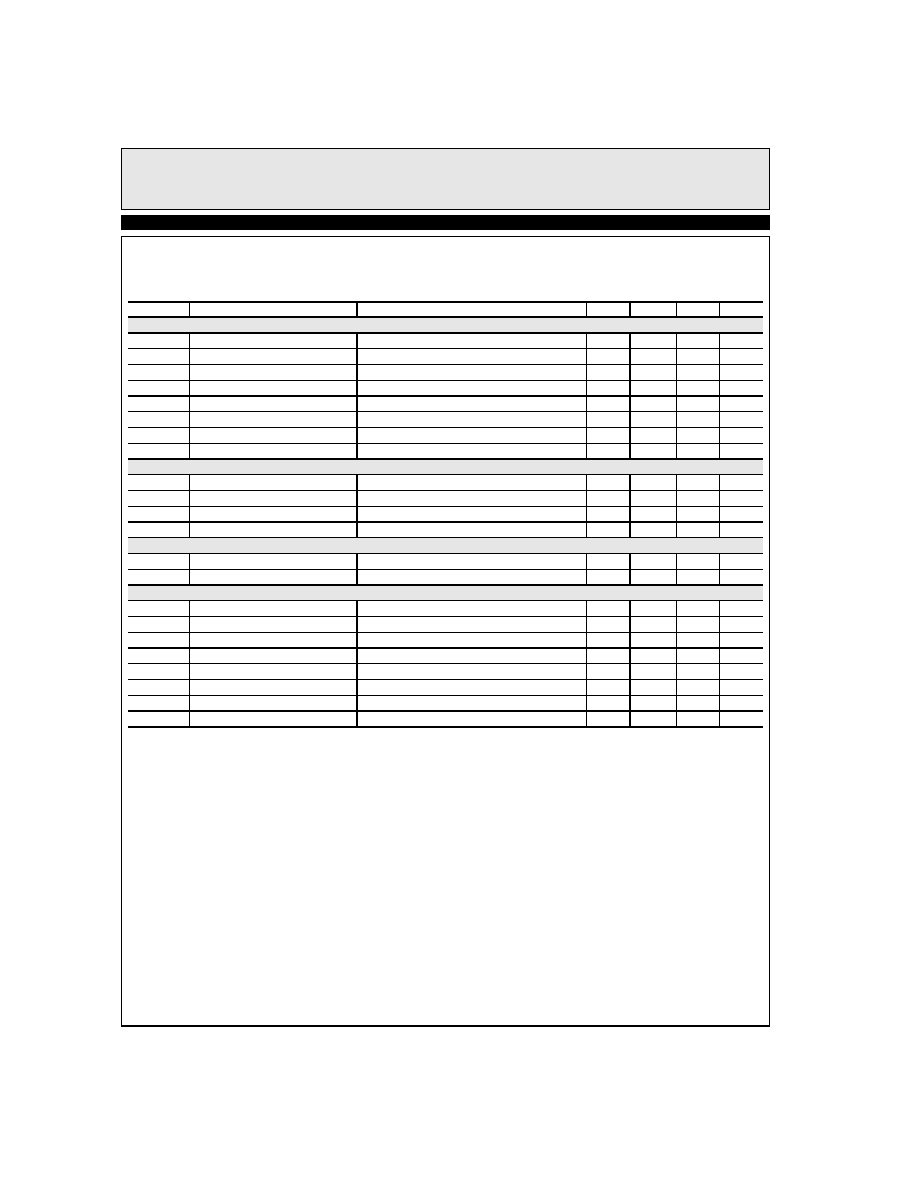
Ordering Information
Part No.
Package
Tape & Reel
Outline #
EL5210CS
8-Pin SOIC
-
MDP0027
EL5210CS-T13
8-Pin SOIC
13"
MDP0027
EL5210CY
8-Pin MSOP
-
MDP0043
EL5210CY-T7
8-Pin MSOP
7"
MDP0043
EL5210CY-T13
8-Pin MSOP
13"
MDP0043
EL5410CS
14-Pin SOIC
-
MDP0027
EL5410CS-T13
14-Pin SOIC
13"
MDP0027
EL5410CR
14-Pin TSSOP
-
MDP0044
EL5410CR-T13
14-Pin TSSOP
13"
MDP0044
EL5210C/EL5410C
30MHz Rail-to-Rail Input-Output Op Amps
Nove
mber 16, 2000

2
EL5210C/EL5410C
30MHz Rail-to-Rail Input-Output Op Amps
E
L
5210C/E
L5410C
Absolute Maximum Ratings
(T
A
= 25įC)
Values beyond absolute maximum ratings can cause the device to be pre-
maturely damaged. Absolute maximum ratings are stress ratings only and
functional device operation is not implied.
Supply Voltage between V
S
+ and V
S
-
+18V
Input Voltage
V
S
- - 0.5V, V
S
+0.5V
Maximum Continuous Output Current
30mA
Maximum Die Temperature
+125įC
Storage Temperature
-65įC to +150įC
Operating Temperature
-40įC to +85įC
Power Dissipation
See Curves
ESD Voltage
2kV
Important Note:
All parameters having Min/Max specifications are guaranteed. Typ values are for information purposes only. Unless otherwise noted, all tests are at the
specified temperature and are pulsed tests, therefore: T
J
= T
C
= T
A
Electrical Characteristics
V
S
+ = +5V, V
S
- = -5V, R
L
= 1k
and C
L
= 12pF to 0V, T
A
= 25įC unless otherwise specified.
Parameter
Description
Condition
Min
Typ
Max
Unit
Input Characteristics
V
OS
Input Offset Voltage
V
CM
= 0V
3
15
mV
TCV
OS
Average Offset Voltage Drift
[1]
7
ĶV/įC
I
B
Input Bias Current
V
CM
= 0V
2
60
nA
R
IN
Input Impedance
1
G
C
IN
Input Capacitance
2
pF
CMIR
Common-Mode Input Range
-5.5
+5.5
V
CMRR
Common-Mode Rejection Ratio
for V
IN
from -5.5V to 5.5V
50
70
dB
A
VOL
Open-Loop Gain
-4.5V
V
OUT
4.5V
65
80
dB
Output Characteristics
V
OL
Output Swing Low
I
L
= -5mA
-4.9
-4.8
V
V
OH
Output Swing High
I
L
= 5mA
4.8
4.9
V
I
SC
Short Circuit Current
Ī120
mA
I
OUT
Output Current
Ī30
mA
Power Supply Performance
PSRR
Power Supply Rejection Ratio
V
S
is moved from Ī2.25V to Ī7.75V
60
80
dB
I
S
Supply Current (Per Amplifier)
No Load
2.5
3.75
mA
Dynamic Performance
SR
Slew Rate
[2]
-4.0V
V
OUT
4.0V, 20% o 80%
33
V/Ķ s
t
S
Settling to +0.1% (A
V
= +1)
(A
V
= +1), V
O
= 2V Step
140
ns
BW
-3dB Bandwidth
30
MHz
GBWP
Gain-Bandwidth Product
20
MHz
PM
Phase Margin
50
į
CS
Channel Separation
f = 5MHz
110
dB
d
G
Differential Gain
[3]
R
F
= R
G
= 1k
and V
OUT
= 1.4V
0.12
%
d
P
Differential Phase
[3]
R
F
= R
G
= 1k
and V
OUT
= 1.4V
0.17
į
1.
Measured over operating temperature range
2.
Slew rate is measured on rising and falling edges
3.
NTSC signal generator used

3
EL5210C/EL5410C
30MHz Rail-to-Rail Input-Output Op Amps
EL
5210C/EL
5410C
Electrical Characteristics
V
S
+ = 5V, V
S
- = 0V, R
L
= 1k
and C
L
= 12pF to 2.5V, T
A
= 25įC unless otherwise specified.
Parameter
Description
Condition
Min
Typ
Max
Unit
Input Characteristics
V
OS
Input Offset Voltage
V
CM
= 2.5V
3
15
mV
TCV
OS
Average Offset Voltage Drift
[1]
7
ĶV/įC
I
B
Input Bias Current
V
CM
= 2.5V
2
60
nA
R
IN
Input Impedance
1
G
C
IN
Input Capacitance
2
pF
CMIR
Common-Mode Input Range
-0.5
+5.5
V
CMRR
Common-Mode Rejection Ratio
for V
IN
from -0.5V to 5.5V
45
66
dB
A
VOL
Open-Loop Gain
0.5V
V
OUT
4.5V
65
80
dB
Output Characteristics
V
OL
Output Swing Low
I
L
= -5mA
100
200
mV
V
OH
Output Swing High
I
L
= 5mA
4.8
4.9
V
I
SC
Short Circuit Current
Ī120
mA
I
OUT
Output Current
Ī30
mA
Power Supply Performance
PSRR
Power Supply Rejection Ratio
V
S
is moved from 4.5V to 15.5V
60
80
dB
I
S
Supply Current (Per Amplifier)
No Load
2.5
3.75
mA
Dynamic Performance
SR
Slew Rate
[2]
1V
V
OUT
4V, 20% o 80%
33
V/Ķs
t
S
Settling to +0.1% (A
V
= +1)
(A
V
= +1), V
O
= 2V Step
140
ns
BW
-3dB Bandwidth
30
MHz
GBWP
Gain-Bandwidth Product
20
MHz
PM
Phase Margin
50
į
CS
Channel Separation
f = 5MHz
110
dB
d
G
Differential Gain
[3]
R
F
= R
G
= 1k
and V
OUT
= 1.4V
0.30
%
d
P
Differential Phase
[3]
R
F
= R
G
= 1k
and V
OUT
= 1.4V
0.66
į
1.
Measured over operating temperature range
2.
Slew rate is measured on rising and falling edges
3.
NTSC signal generator used
4
EL5210C/EL5410C
30MHz Rail-to-Rail Input-Output Op Amps
E
L
5210C/E
L5410C
Electrical Characteristics
V
S
+ = 15V, V
S
- = 0V, R
L
= 1k
and C
L
= 12pF to 7.5V, T
A
= 25įC unless otherwise specified.
Parameter
Description
Condition
Min
Typ
Max
Unit
Input Characteristics
V
OS
Input Offset Voltage
V
CM
= 7.5V
3
15
mV
TCV
OS
Average Offset Voltage Drift
[1]
7
ĶV/įC
I
B
Input Bias Current
V
CM
= 7.5V
2
60
nA
R
IN
Input Impedance
1
G
C
IN
Input Capacitance
2
pF
CMIR
Common-Mode Input Range
-0.5
+15.5
V
CMRR
Common-Mode Rejection Ratio
for V
IN
from -0.5V to 15.5V
53
72
dB
A
VOL
Open-Loop Gain
0.5V
V
OUT
14.5V
65
80
dB
Output Characteristics
V
OL
Output Swing Low
I
L
= -7.5mA
170
350
mV
V
OH
Output Swing High
I
L
= 7.5mA
14.65
14.83
V
I
SC
Short Circuit Current
Ī120
mA
I
OUT
Output Current
Ī30
mA
Power Supply Performance
PSRR
Power Supply Rejection Ratio
V
S
is moved from 4.5V to 15.5V
60
80
dB
I
S
Supply Current (Per Amplifier)
No Load
2.5
3.75
mA
Dynamic Performance
SR
Slew Rate
[2]
1V
V
OUT
14V, 20% o 80%
33
V/Ķ s
t
S
Settling to +0.1% (A
V
= +1)
(A
V
= +1), V
O
= 2V Step
140
ns
BW
-3dB Bandwidth
30
MHz
GBWP
Gain-Bandwidth Product
20
MHz
PM
Phase Margin
50
į
CS
Channel Separation
f = 5MHz
110
dB
d
G
Differential Gain
[3]
R
F
= R
G
= 1k
and V
OUT
= 1.4V
0.10
%
d
P
Differential Phase
[3]
R
F
= R
G
= 1k
and V
OUT
= 1.4V
0.11
į
1.
Measured over operating temperature range
2.
Slew rate is measured on rising and falling edges
3.
NTSC signal generator used
5
EL5210C/EL5410C
30MHz Rail-to-Rail Input-Output Op Amps
EL
5210C/EL
5410C
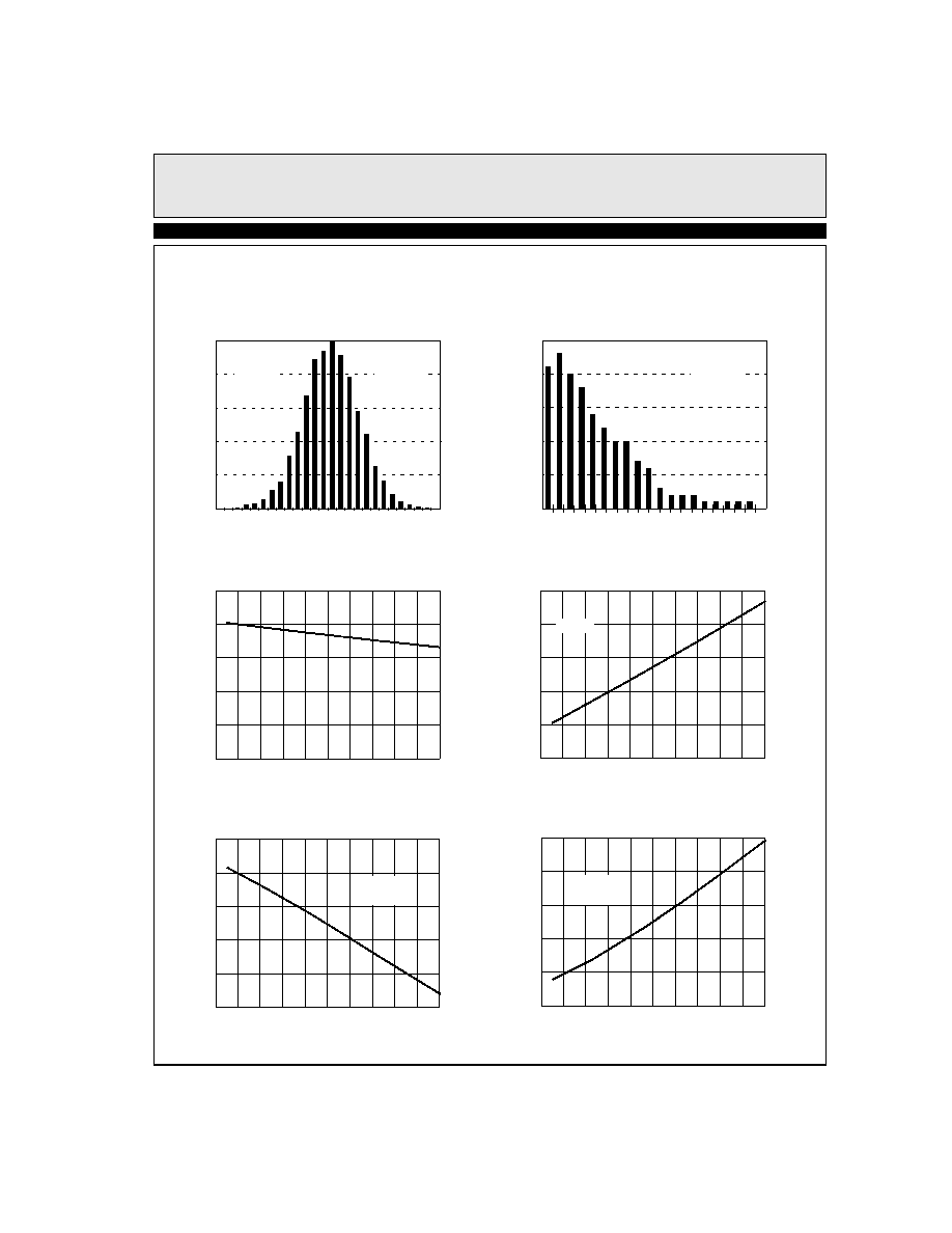
Typical Performance Curves
Input Bias Current vs Temperature
0
I
n
put
B
i
as
C
u
rre
nt
(Ķ
A
)
Temperature (įC)
-0.008
0.008
-0.004
-0.012
0.004
-50
-10
30
70
110
150
Output High Voltage vs Temperature
4.92
4.93
Out
put
Hi
gh V
o
l
t
a
ge (V
)
4.91
4.96
Output Low Voltage vs Temperature
-4.91
-4.87
Out
put
Low V
o
l
t
a
ge (V
)
-4.95
-4.85
Temperature (įC)
4.94
Temperature (įC)
-4.89
-4.93
-50
-10
30
70
110
150
4.95
-50
-10
30
70
110
150
V
S
=Ī5V
I
OUT
=5mA
V
S
=Ī5V
I
OUT
=5mA
Input Offset Voltage vs Temperature
1
2
I
npu
t
Of
f
s
et
V
o
l
t
age (m
V
)
Temperature (įC)
0
3
-50
-10
30
70
110
150
4
5
EL5410C Input Offset Voltage Distribution
200
Qu
a
n
t
i
t
y
(
A
mp
lif
ie
r
s
)
Input Offset Voltage (mV)
0
-1
2
500
400
100
300
-1
0
-8
-6
-4
-2
-0
2
4
6
8
10
12
Input Offset Voltage Drift, TCV
OS
(Ķ V/įC)
1
3
5
7
9
11
13
15
17
19
21
5
Qu
a
n
t
i
t
y
(
A
mp
lif
ie
r
s
)
0
25
15
20
10
EL5410C Input Offset Voltage Drift
V
S
=Ī5V
Typical
Production
Distortion
Typical
Production
Distortion
V
S
=Ī5V
T
A
=25įC
V
S
=Ī5V

6
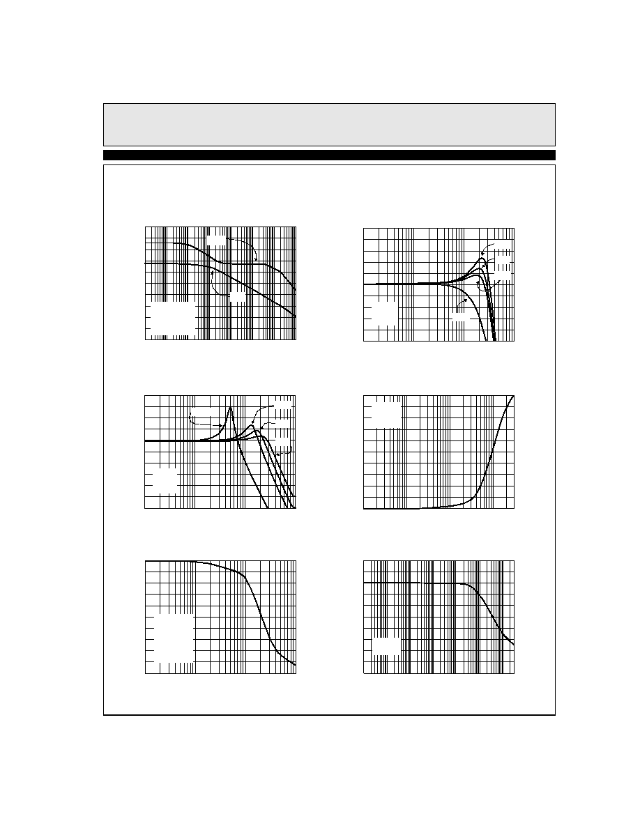
EL5210C/EL5410C
30MHz Rail-to-Rail Input-Output Op Amps
E
L
5210C/E
L5410C
Typical Performance Curves
Open-Loop Gain vs Temperature
75
85
Op
en-L
oop Gai
n
(d
B
)
90
Temperature (įC)
-50
-10
30
70
110
150
70
80
Slew Rate vs Temperature
V
S
=Ī5V
R
L
=1k
EL5410C Supply Current per Amplifier vs
Temperature
2.45
2.5
Su
p
p
ly
C
u
r
r
e
n
t
(
m
A)
2.4
Temperature (įC)
-50
-10
30
70
110
150
2.6
2.65
2.55
2.7
V
S
=Ī5V
EL5410C Supply Current per Amplifier vs Supply
Voltage
4
1.7
2.5
Su
p
p
ly
C
u
r
r
e
n
t
(
m
A)
Supply Voltage (V)
1.5
2.9
2.1
2.3
2.7
1.9
8
12
16
20
T
A
=25įC
160
33.70
33.75
Sl
e
w
R
a
t
e
(
V
/Ķ
S
)
Temperature (įC)
33.65
33.85
33.60
33.55
120
80
40
0
-40
33.80
0.05
-0.05
0.15
D
i
ff
G
a
i
n
(%)
D
i
ff
Ph
a
s
e
(
į
)
Differential Gain and Phase
0.25
0
-0.10
0.10
0.20
200
IRE
0
100
200
0
100
Harmonic Distortion vs V
OP-P
0
4
10
-60
-30
-80
2
6
8
-40
-70
-50
V
OP-P
(V)
Di
s
t
or
t
i
on
(
d
B
)
V
S
=Ī5V
V
S
=Ī5V
A
V
=2
R
L
=1k
V
S
=Ī5V
A
V
=1
R
L
=1k
F
IN
= 1MHz
HD3
HD2
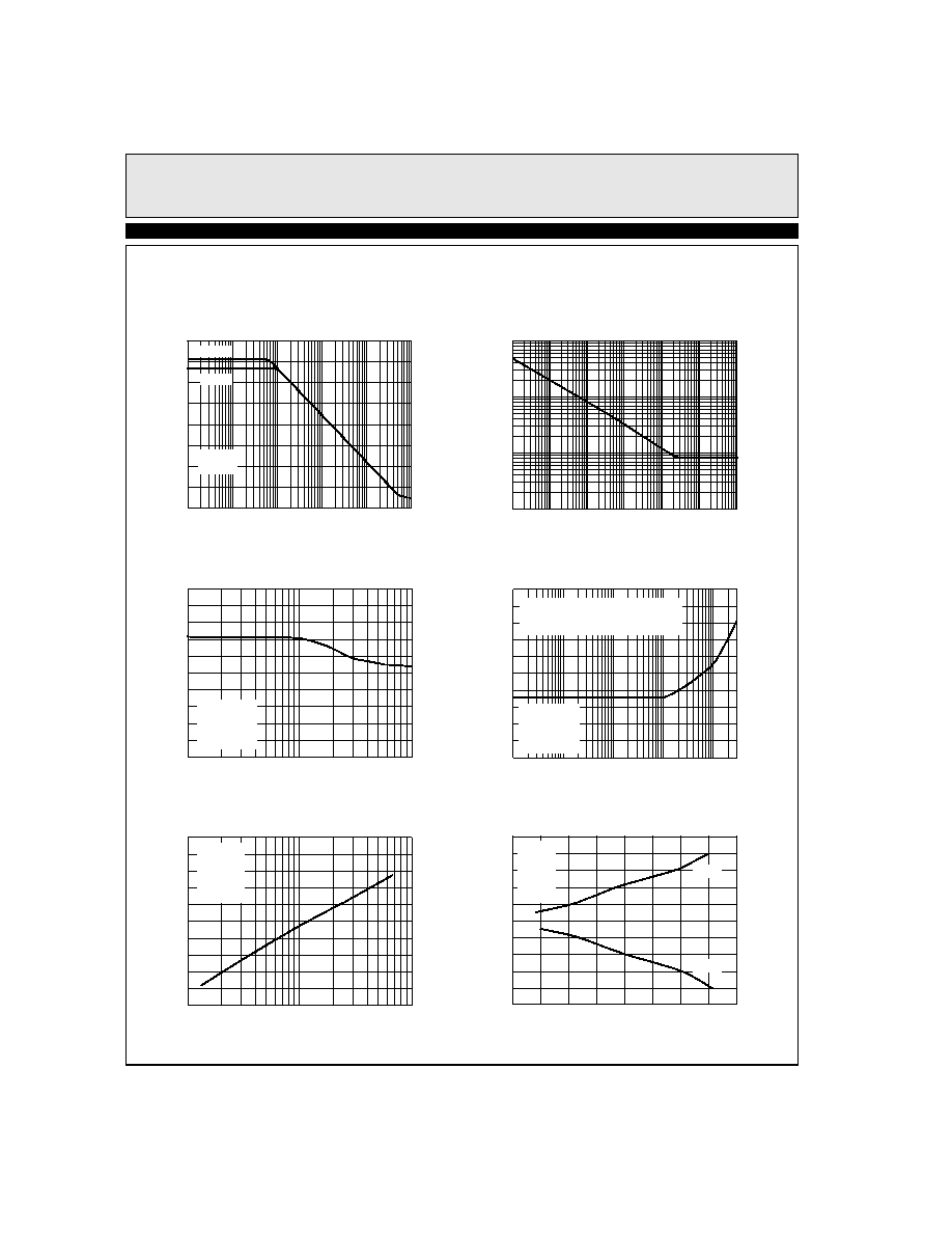
7
EL5210C/EL5410C
30MHz Rail-to-Rail Input-Output Op Amps
EL
5210C/EL
5410C
Typical Performance Curves
Open Loop Gain and Phase vs Frequency
10
10k
100M
20
140
Frequency (Hz)
-60
Gain (d
B
)
P
has
e (
į
)
100
1k
100k
1M
10M
100
-20
60
-50
250
-250
150
-150
50
Frequency Response for Various R
L
1M
100M
-1
1
M
agni
t
ude
(
N
or
m
a
l
i
z
ed)
(
d
B
)
Frequency (Hz)
-5
10M
100k
3
-3
5
Phase
Gain
0
1M
100M
Frequency (Hz)
10M
100k
0
10
M
agni
t
ude (N
orm
a
l
i
z
ed) (d
B
)
-30
20
-20
-10
Frequency Response for Various C
L
Closed Loop Output Impedance vs Frequency
Ou
t
p
ut
I
m
p
edanc
e (
)
Frequency (Hz)
10k
100k
0
40
80
120
200
1M
160
30M
10M
R
L
=1k
A
V
=1
V
S
=Ī5V
A
V
=1
V
S
=Ī5V
T
A
=25įC
CMRR vs Frequency
30
CM
RR
(
d
B
)
Frequency (Hz)
80
70
60
40
50
10
100
1k
10k
100k
1M
10M 30M
V
S
=Ī5V
T
A
=25įC
Maximum Output Swing vs Frequency
M
a
x
i
mu
m
Ou
tp
u
t
Sw
in
g
(
V
P-
P
)
Frequency (Hz)
10k
100k
0
2
4
1M
6
10M
8
10
V
S
=Ī5V
T
A
=25įC
A
V
=1
R
L
=1k
C
L
=12pF
Distortion <1%
V
S
=Ī5V
T
A
=25įC
R
L
=1k
to GND
C
L
=12pF to GND
1k
560
150
10k
A
V
=1
V
S
=Ī5V
C
L
=12pF
100pF
47pF
10pF
1000pF
8
EL5210C/EL5410C
30MHz Rail-to-Rail Input-Output Op Amps
E
L
5210C/E
L5410C
Typical Performance Curves
Settling Time vs Step Size
230
-2
2
St
e
p
Siz
e
(
V
)
Settling Time (ns)
4
3
1
-3
0
-1
-4
5
-5
70
210
190
170
150
130
110
90
V
S
=Ī5V
A
V
=1
R
L
=1k
C
L
=12pF
T
A
=25įC
PSRR vs Frequency
100
0
P
S
RR (d
B)
Frequency (Hz)
80
60
40
20
1M
10M
10k
100k
V
S
=Ī5V
T
A
=25įC
1k
PSRR+
PSRR-
Input Voltage Noise Spectral Density vs
Frequency
100
100k
100M
10
100
V
o
l
t
ag
e N
o
i
s
e
(
nV
Hz
)
Frequency (Hz)
1
10M
1k
10k
1M
1000
1k
10k
100k
0.008
Total Harmonic Distortion + Noise vs Frequency
Frequency (Hz)
T
H
D+
N (%
)
Channel Separation vs Frequency Response
1k
-60
XT
a
l
k
(
d
B)
Frequency (Hz)
-160
-120
-100
-80
0.010
1M
30M
10k
100k
0.006
0.004
0.002
10M
Dual measured Channel A to B
Quad measured Channel A to D or B to C
Other combinations yield improved rejection
0
V
S
=Ī5V
R
L
=1k
A
V
=1
V
IN
=0.5V
RMS
V
S
=Ī5V
R
L
=1k
A
V
=1
V
IN
=110mV
RMS
10
100
1000
Small-Signal Overshoot vs Load Capacitance
Load Capacitance (pF)
Ov
ers
hoo
t
(%
)
0
20
40
60
80
100
V
S
=Ī5V
A
V
=1
R
L
=1k
V
IN
=Ī50mV
T
A
=25įC
-140
0.1%
0.1%
9
EL5210C/EL5410C
30MHz Rail-to-Rail Input-Output Op Amps
EL
5210C/EL
5410C
Typical Performance Curves
Large Signal Transient Response
Small Signal Transient Response
V
S
=Ī5V
T
A
=25įC
A
V
=1
R
L
=1k
C
L
=12pF
1V
200ns
50mV
100nS
V
S
=Ī5V
T
A
=25įC
A
V
=1
R
L
=1k
C
L
=12pF
10
EL5210C/EL5410C
30MHz Rail-to-Rail Input-Output Op Amps
E
L
5210C/E
L5410C
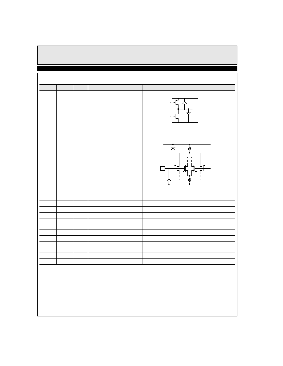
Pin Descriptions
EL5210C
EL5410C
Name
Function
Equivalent Circuit
1
1
V
OUTA
Amplifier A Output
2
2
V
INA-
Amplifier A Inverting Input
3
3
V
INA+
Amplifier A Non-Inverting Input
(Reference Circuit 2)
8
4
V
S+
Positive Power Supply
5
5
V
INB+
Amplifier B Non-Inverting Input
(Reference Circuit 2)
6
6
V
INB-
Amplifier B Inverting Input
(Reference Circuit 2)
7
7
V
OUTB
Amplifier B Output
(Reference Circuit 1)
8
V
OUTC
Amplifier C Output
(Reference Circuit 1)
9
V
INC-
Amplifier C Inverting Input
(Reference Circuit 2)
10
V
INC+
Amplifier C Non-Inverting Input
(Reference Circuit 2)
4
11
V
S-
Negative Power Supply
12
V
IND+
Amplifier D Non-Inverting Input
(Reference Circuit 2)
13
V
IND-
Amplifier D Inverting Input
(Reference Circuit 2)
14
V
OUTD
Amplifier D Output
(Reference Circuit 1)
V
S+
GND
V
S-
Circuit 1
V
S+
V
S-
Circuit 2

11
EL5210C/EL5410C
30MHz Rail-to-Rail Input-Output Op Amps
EL
5210C/EL
5410C
Applications Information
Product Description
The EL5210C and EL5410C voltage feedback amplifi-
ers are fabricated using a high voltage CMOS process.
They exhibit Rail-to-Rail input and output capability,
are unity gain stable and have low power consumption
(2.5mA per amplifier). These features make the
EL5210C and EL5410C ideal for a wide range of gen-
eral-purpose applications. Connected in voltage follower
mode and driving a load of 1k
and 12pF, the EL5210C
and EL5410C have a -3dB bandwidth of 30MHz while
maintaining a 33V/ĶS slew rate. The EL5210C is a dual
amplifier while the EL5410C is a quad amplifier.
Operating Voltage, Input, and Output
The EL5210C and EL5410C are specified with a single
nominal supply voltage from 5V to 15V or a split supply
with its total range from 5V to 15V. Correct operation is
guaranteed for a supply range of 4.5V to 16.5V. Most
EL5210C and EL5410C specifications are stable over
both the full supply range and operating temperatures of
-40 įC to +85 įC. Parameter variations with operating
voltage and/or temperature are shown in the typical per-
formance curves.
The input common-mode voltage range of the EL5210C
and EL5410C extends 500mV beyond the supply rails.
The output swings of the EL5210C and EL5410C typi-
cally extend to within 100mV of positive and negative
supply rails with load currents of 5mA. Decreasing load
currents will extend the output voltage range even closer
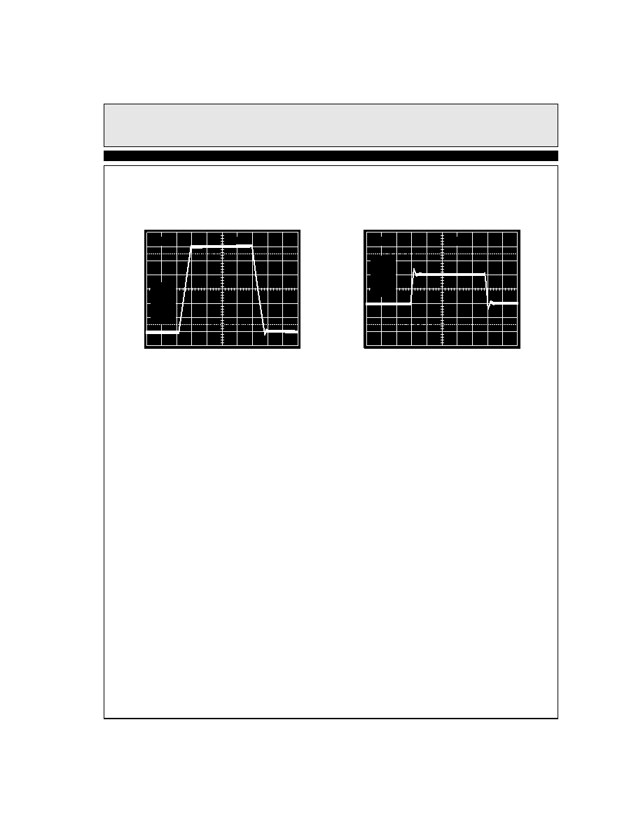
to the supply rails. Figure 1 shows the input and output
waveforms for the device in the unity-gain configura-
tion. Operation is from +/-5V supply with a 1k
load
connected to GND. The input is a 10Vp-p sinusoid. The
output voltage is approximately 9.8V
P-P
.
Figure 1. Operation with Rail-to-Rail Input and
Output
Short Circuit Current Limit
The EL5210C and EL5410C will limit the short circuit
current to +/-120mA if the output is directly shorted to
the positive or the negative supply. If an output is
shorted indefinitely, the power dissipation could easily
increase such that the device may be damaged. Maxi-
mum reliability is maintained if the output continuous
current never exceeds +/-30mA. This limit is set by the
design of the internal metal interconnects.
Output Phase Reversal
The EL5210C and EL5410C are immune to phase rever-
sal as long as the input voltage is limited from V
S
- -
0.5V to V
S
+ +0.5V. Figure 2 shows a photo of the out-
put of the device with the input voltage driven beyond
the supply rails. Although the device's output will not
change phase, the input's overvoltage should be avoided.
If an input voltage exceeds supply voltage by more than
0.6V, electrostatic protection diodes placed in the input
V
S
=Ī5V
T
A
=25įC
A
V
=1
V
IN
=10V
P-P
Out
put
I
n
p
u
t
5V
5V
10Ķ S

12
EL5210C/EL5410C
30MHz Rail-to-Rail Input-Output Op Amps
E
L
5210C/E
L5410C
stage of the device begin to conduct and overvoltage
damage could occur.
Figure 2. Operation with Beyond-the-Rails
Input
Power Dissipation
With the high-output drive capability of the EL5210C
and EL5410C amplifiers, it is possible to exceed the
125įC 'absolute-maximum junction temperature' under
certain load current conditions. Therefore, it is important
to calculate the maximum junction temperature for the
application to determine if load conditions need to be
modified for the amplifier to remain in the safe operating
area.
The maximum power dissipation allowed in a package is
determined according to:
Where:
T
JMAX
= Maximum Junction Temperature
T
AMAX
= Maximum Ambient Temperature
JA
= Thermal Resistance of the Package
P
DMAX
= Maximum Power Dissipation in the
Package.
The maximum power dissipation actually produced by
an IC is the total quiescent supply current times the total
power supply voltage, plus the power in the IC due to the
loads, or:
when sourcing, and
when sinking.
Where:
i = 1 to 2 for Dual and 1 to 4 for Quad
V
S
= Total Supply Voltage
I
SMAX
= Maximum Supply Current Per Amplifier
V
OUT
i = Maximum Output Voltage of the
Application
I
LOAD
i = Load current
If we set the two P
DMAX
equations equal to each other,
we can solve for R
LOAD
i to avoid device overheat. Fig-
ure 3 and Figure 4 provide a convenient way to see if the
device will overheat. The maximum safe power dissipa-
tion can be found graphically, based on the package type
and the ambient temperature. By using the previous
equation, it is a simple matter to see if P
DMAX
exceeds
the device's power derating curves. To ensure proper
operation, it is important to observe the recommended
derating curves shown in Figure 3 and Figure 4.
V
S
=Ī2.5V
T
A
=25įC
A
V
=1
V
IN
=6V
P-P
1V
1V
10Ķ S
P
D MAX
T
JM AX
T
A MA X
≠
JA
---------------------------------------------
=
P
D MAX
i V
[
S
I
SMA X
V
(
S
+
V
OU T
i
) I
L OA D
i
◊
≠
+
◊
]
=
P
D MA X
i V
[
S
I
SM AX
V
(
OU T
i
V
S
-
) I
L OA D
i
◊
≠
+
◊
]
=

13
EL5210C/EL5410C
30MHz Rail-to-Rail Input-Output Op Amps
EL
5210C/EL
5410C
Figure 3. Package Power Dissipation vs
Ambient Temperature
Figure 4. Package Power Dissipation vs
Ambient Temperature
Unused Amplifiers
It is recommended that any unused amplifiers in a dual
and a quad package be configured as a unity gain fol-
lower. The inverting input should be directly connected
to the output and the non-inverting input tied to the
ground plane.
Driving Capacitive Loads
The EL5210C and EL5410C can drive a wide range of
capacitive loads. As load capacitance increases, how-
ever, the -3dB bandwidth of the device will decrease and
the peaking increase. The amplifiers drive 10pF loads in
parallel with 1k
with just 1.2dB of peaking, and 100pF
with 6.5dB of peaking. If less peaking is desired in these
applications, a small series resistor (usually between 5
and 50
) can be placed in series with the output. How-
ever, this will obviously reduce the gain slightly.
Another method of reducing peaking is to add a "snub-
ber" circuit at the output. A snubber is a shunt load
consisting of a resistor in series with a capacitor. Values
of 150
and 10nF are typical. The advantage of a snub-
ber is that it does not draw any DC load current or
reduce the gain
Power Supply Bypassing and Printed Circuit
Board Layout
The EL5210C and EL5410C can provide gain at high
frequency. As with any high-frequency device, good
printed circuit board layout is necessary for optimum
performance. Ground plane construction is highly rec-
ommended, lead lengths should be as short as possible
and the power supply pins must be well bypassed to
reduce the risk of oscillation. For normal single supply
operation, where the V
S
- pin is connected to ground, a
0.1ĶF ceramic capacitor should be placed from V
S
+ to
pin to V
S
- pin. A 4.7ĶF tantalum capacitor should then
be connected in parallel, placed in the region of the
amplifier. One 4.7ĶF capacitor may be used for multiple
devices. This same capacitor combination should be
placed at each supply pin to ground if split supplies are
to be used.
50
150
400
800
P
o
wer
D
i
s
s
i
pat
i
on
(m
W)
Ambient Temperature (įC)
0
100
0
1200
25
75
1000
600
200
125
85
MAX T
J
=125įC
TSSOP14
JA
=100įC/W
SO8
JA
=110įC/W
Packages Mounted on a JEDEC JESD51-7 High
Effective Thermal Conductivity Test Board
1.0W
1.136W
909mW
833mW
SO14
JA
=88įC/W
MSOP8
JA
=115įC/W
50
150
400
800
P
o
w
e
r
D
i
s
s
ip
a
t
io
n
(
m
W
)
Ambient Temperature (įC)
0
100
0
125
1200
25
75
1000
600
200
85
MAX T
J
=125įC
TSSOP14
JA
=165įC/W
SO8
JA
=160įC/W
MSOP8
JA
=206įC/W
SO14
JA
=120įC/W
Packages Mounted on a JEDEC JESD51-3 Low
Effective Thermal Conductivity Test Board
833mW
606mW
625mW
485mW
14
EL5210C/EL5410C
30MHz Rail-to-Rail Input-Output Op Amps
E
L
5210C/E
L5410C
General Disclaimer
Specifications contained in this data sheet are in effect as of the publication date shown. Elantec, Inc. reserves the right to make changes in the cir-
cuitry or specifications contained herein at any time without notice. Elantec, Inc. assumes no responsibility for the use of any circuits described
herein and makes no representations that they are free from patent infringement.
WARNING - Life Support Policy
Elantec, Inc. products are not authorized for and should not be used
within Life Support Systems without the specific written consent of
Elantec, Inc. Life Support systems are equipment intended to sup-
port or sustain life and whose failure to perform when properly used
in accordance with instructions provided can be reasonably
expected to result in significant personal injury or death. Users con-
templating application of Elantec, Inc. Products in Life Support
Systems are requested to contact Elantec, Inc. factory headquarters
to establish suitable terms & conditions for these applications. Elan-
tec, Inc.'s warranty is limited to replacement of defective
components and does not cover injury to persons or property or
other consequential damages.
Novem
b
e
r
16, 2000
Printed in U.S.A.
Elantec Semiconductor, Inc.
675 Trade Zone Blvd.
Milpitas, CA 95035
Telephone: (408) 945-1323
(888) ELANTEC
Fax:
(408) 945-9305
European Office: +44-118-977-6080
Japan Technical Center: +81-45-682-5820