 | –≠–ª–µ–∫—Ç—Ä–æ–Ω–Ω—ã–π –∫–æ–º–ø–æ–Ω–µ–Ω—Ç: EL5393CU | –°–∫–∞—á–∞—Ç—å:  PDF PDF  ZIP ZIP |
Note: All information contained in this data sheet has been carefully checked and is believed to be accurate as of the date of publication; however, this data sheet cannot be a "controlled document". Current revisions, if any, to these
specifications are maintained at the factory and are available upon your request. We recommend checking the revision level before finalization of your design documentation.
© 2001 Elantec Semiconductor, Inc.
EL
5393C
General Description
The EL5393C is a triple current feedback amplifier with a bandwidth
of 300MHz. This makes these amplifiers ideal for today's high speed
video and monitor applications.
With a supply current of just 4mA per amplifier and the ability to run
from a single supply voltage from 5V to 10V, these amplifiers are also
ideal for hand held, portable or battery powered equipment.
For applications where board space is critical, the EL5393C is offered
in 16-pin QSOP package, as well as an industry standard 16-pin SO.
The EL5393C operates over the industrial temperature range of -40
∞
C
to +85
∞
C.
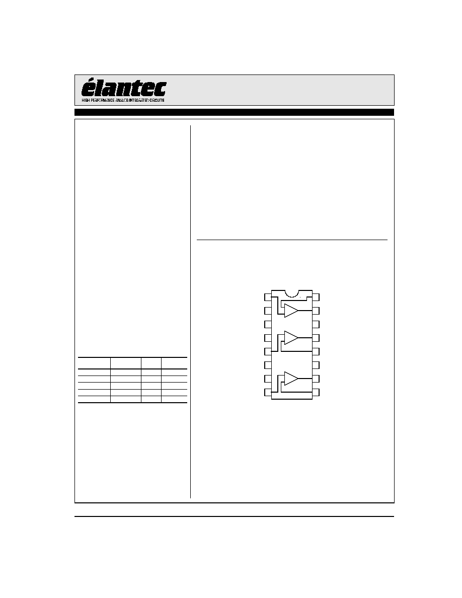
Pin Configurations
1
2
3
4
16
15
14
13
5
6
7
12
11
10
8
9
VS+
OUTA
OUTB
INA-
OUTC
NC
INC-
INB-
NC*
VS-
NC*
INA+
NC
NC*
INC+
INB+
16-Pin SO & QSOP
EL5393CS, EL5393CU
-
+
-
+
-
+
Features
∑ 300MHz -3dB bandwidth
∑ 4mA supply current (per amplifier)
∑ Single and dual supply operation,
from 5V to 10V
∑ Available in 16-pin QSOP package
∑ Single (EL5193C) and Dual
(EL5293C) available
∑ High speed, 1GHz product
available (EL5191C)
∑ High speed, 6mA, 600MHz
product available (EL5192C,
EL5292C, and EL5392C
Applications
∑ Battery-powered Equipment
∑ Hand-held, Portable Devices
∑ Video Amplifiers
∑ Cable Drivers
∑ RGB Amplifiers
∑ Test Equipment
∑ Instrumentation
∑ Current to Voltage Converters
Ordering Information
Part No
Package
Tape &
Reel
Outline #
EL5393CS
16-Pin SO
-
MDP0027
EL5393CS-T7
16-Pin SO
7"
MDP0027
EL5393CS-T13
16-Pin SO
13"
MDP0027
EL5393CU
16-Pin QSOP
-
MDP0040
EL5393CU-T13
16-Pin QSOP
13"
MDP0040
EL5393C
Triple 300MHz Current Feedback Amplifier
Ap
r
i
l 26, 2001

2
EL5393C
Triple 300MHz Current Feedback Amplifier
E
L
5393C
Absolute Maximum Ratings
(T
A
= 25∞C)
Values beyond absolute maximum ratings can cause the device to be pre-
maturely damaged. Absolute maximum ratings are stress ratings only and
functional device operation is not implied.
Supply Voltage between V
S
+ and V
S
-
11V
Maximum Continuous Output Current
50mA
Operating Junction Temperature
125∞C
Power Dissipation
See Curves
Pin Voltages
V
S
- - 0.5V to V
S
+ +0.5V
Storage Temperature
-65∞C to +150∞C
Operating Temperature
-40∞C to +85∞C
Important Note:
All parameters having Min/Max specifications are guaranteed. Typ values are for information purposes only. Unless otherwise noted, all tests are at the
specified temperature and are pulsed tests, therefore: T
J
= T
C
= T
A
.
Electrical Characteristics
V
S
+ = +5V, V
S
- = -5V, R
F
= 750
for A
V
= 1, R
F
= 375
for A
V
= 2, R
L
= 150
, T
A
= 25∞C unless otherwise specified.
Parameter
Description
Conditions
Min
Typ
Max
Unit
AC Performance
BW
-3dB Bandwidth
A
V
= +1
300
MHz
A
V
= +2
200
MHz
BW1
0.1dB Bandwidth
20
MHz
SR
Slew Rate
V
O
=-2.5V to +2.5V, A
V
= +2
2000
2200
V/µs
ts
0.1% Settling Time
V
OUT
= -2.5V to +2.5V, A
V
= -1
12
ns
C
S
Channel Separation
f = 5MHz
60
dB
e
n
Input Voltage Noise
4.4
nV/
Hz
i
n
-
IN- input current noise
17
pA/
Hz
i
n
+
IN+ input current noise
50
pA/
Hz
dG
Differential Gain Error
[1]
A
V
= +2
0.03
%
dP
Differential Phase Error
[1]
A
V
= +2
0.04
∞
DC Performance
V
OS
Offset Voltage
-10
1
10
mV
T
C
V
OS
Input Offset Voltage Temperature Coefficient
Measured from T
MIN
to T
MAX
5
µV/∞C
R
OL
Transimpedance
300
600
k
Input Characteristics
CMIR
Common Mode Input Range
±3
±3.3
V
CMRR
Common Mode Rejection Ratio
42
50
dB
+I
IN
+ Input Current
-60
1
60
µA
-I
IN
- Input Current
-35
1
35
µA
R
IN
Input Resistance
45
k
C
IN
Input Capacitance
0.5
pF
Output Characteristics
V
O
Output Voltage Swing
R
L
= 150
to GND
±3.4
±3.7
V
R
L
= 1k
to GND
±3.8
±4.0
V
I
OUT
Output Current
R
L
= 10
to GND
95
120
mA
Supply
Is
ON
Supply Current
No Load, V
IN
= 0V
3
4
5
mA
PSRR
Power Supply Rejection Ratio
DC, V
S
= ±4.75V to ±5.25V
55
75
dB
-IPSR
- Input Current Power Supply Rejection
DC, V
S
= ±4.75V to ±5.25V
-2
2
µA/V
1.
Standard NTSC test, AC signal amplitude = 286mV
p-p
, f = 3.58MHz

3
EL5393C
Triple 300MHz Current Feedback Amplifier
EL
5393C
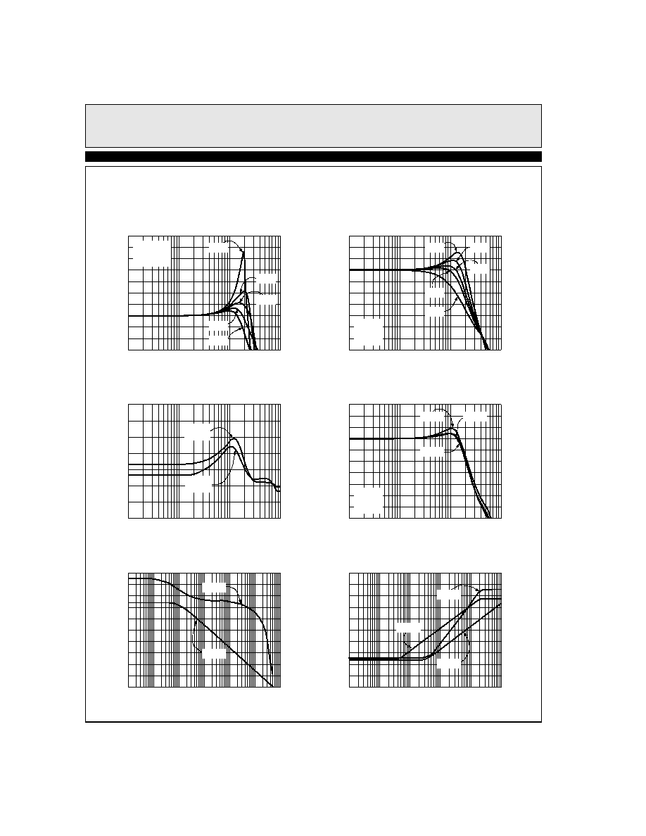
Typical Performance Curves
Non-Inverting Frequency Response (Gain)
1M
10M
100M
1G
6
2
-2
-6
-10
-14
Frequency (Hz)
No
rm
al
i
z
e
d
M
a
gni
t
ude
(dB
)
A
V
=2
A
V
=5
A
V
=10
A
V
=1
R
F
=750
R
L
=150
Non-Inverting Frequency Response (Phase)
1M
10M
100M
1G
90
0
-90
-180
-270
-360
Frequency (Hz)
P
has
e (∞
)
A
V
=2
A
V
=5
A
V
=10
A
V
=1
R
F
=750
R
L
=150
Inverting Frequency Response (Gain)
1M
10M
100M
1G
6
2
-2
-6
-10
-14
Frequency (Hz)
N
o
rm
al
i
z
ed M
agni
t
ude (d
B
)
A
V
=-2
A
V
=-3
A
V
=-1
R
F
=500
R
L
=150
Inverting Frequency Response (Phase)
1M
10M
100M
1G
90
0
-90
-180
-270
-360
Frequency (Hz)
Ph
a
s
e
(
∞
)
A
V
=-2
A
V
=-3
A
V
=-1
R
F
=500
R
L
=150
Frequency Response for Various R
L
1M
10M
100M
1G
6
2
-2
-6
-10
-14
Frequency (Hz)
Nor
m
al
i
z
ed M
agn
i
t
ud
e
(
d
B
)
A
V
=2
R
F
=500
R
L
=100
R
L
=500
R
L
=150
Frequency Response for Various C
IN
-
1M
10M
100M
1G
10
6
2
-2
-6
-10
Frequency (Hz)
Nor
m
al
i
z
ed M
agn
i
t
ud
e
(
d
B
)
A
V
=2
R
F
=500
R
L
=150
0pF added
2pF added
1pF added
4
EL5393C
Triple 300MHz Current Feedback Amplifier
E
L
5393C
Typical Performance Curves
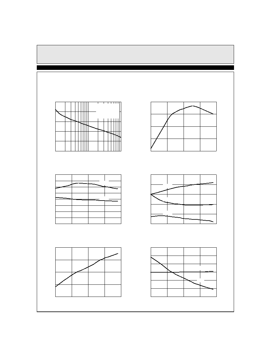
Frequency Response for Various C
L
1M
10M
100M
1G
14
10
6
2
-2
-6
Frequency (Hz)
No
rm
al
i
z
e
d
M
a
gni
t
ude
(dB
)
A
V
=2
R
L
=150
R
F
=R
G
=500
33pF
22pF
15pF
8pF
0pF
Group Delay vs Frequency
1M
10M
100M
1G
Frequency (Hz)
De
l
a
y (n
s
)
A
V
=1
R
F
=750
A
V
=2
R
F
=500
Frequency Response for Various Common-mode
Input Voltages
1M
10M
100M
1G
6
2
-2
-6
-10
-14
Frequency (Hz)
N
o
rm
al
i
z
ed M
agni
t
ude (d
B
)
A
V
=2
R
F
=500
R
L
=150
V
CM
=3V
V
CM
=0V
V
CM
=-3V
3.5
0
3
2.5
2
1.5
1
0.5
Frequency Response for Various R
F
1M
10M
100M
1G
6
2
-2
-6
-10
-14
Frequency (Hz)
No
rm
al
i
z
e
d
M
a
gni
t
ude
(dB
)
A
V
=2
R
G
=R
F
R
L
=150
340
475
620
750
1.2k
Transimpedance (ROL) vs Frequency
1k
Frequency (Hz)
10k
100k
1M
10M
100M
1G
10M
100
1k
10k
100k
1M
Phase
Gain
PSRR and CMRR vs Frequency
PS
RR
/C
M
RR (d
B)
Frequency (Hz)
PSRR+
PSRR-
CMRR
M
a
g
n
i
t
ud
e (
)
20
-80
-60
-40
-20
0
10k
100k
1M
10M
1G
100M
-90
-180
-270
-360
0
Ph
a
s
e
(
∞
)

5
EL5393C
Triple 300MHz Current Feedback Amplifier
EL
5393C
Typical Performance Curves
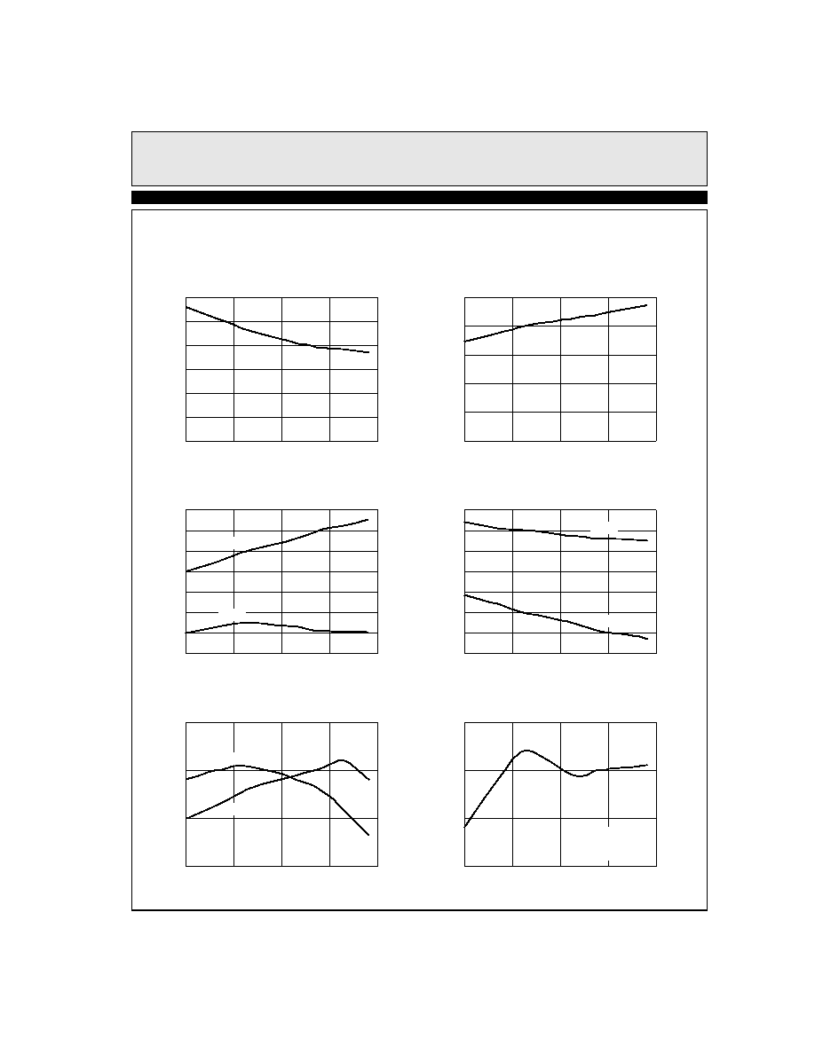
-3dB Bandwidth vs Supply Voltage for Non-
inverting Gains
5
6
9
10
400
200
150
100
50
0
Total Supply Voltage (V)
-3d
B
B
andw
i
d
t
h
(M
H
z
)
A
V
=2
A
V
=5
A
V
=10
A
V
=1
R
F
=750
R
L
=150
Peaking vs Supply Voltage for Non-inverting Gains
4
3.5
2
1
0.5
0
Total Supply Voltage (V)
P
e
a
k
i
ng (d
B
)
A
V
=2
A
V
=1
R
F
=750
R
L
=150
-3dB Bandwidth vs Supply Voltage for Inverting
Gains
250
200
150
100
0
Total Supply Voltage (V)
-3d
B
B
andw
i
d
t
h
(M
H
z
)
A
V
=-2
A
V
=-5
A
V
=-1
R
F
=500
R
L
=150
350
7
8
5
6
9
10
7
8
5
6
9
10
7
8
300
250
50
A
V
=10
2.5
1.5
3
Peaking vs Supply Voltage for Inverting Gains
2.5
2
1.5
1
0.5
0
Total Supply Voltage (V)
P
e
a
k
i
ng (d
B
)
A
V
=-2
A
V
=-1
R
F
=500
R
L
=150
5
6
9
10
7
8
-3dB Bandwidth vs Temperature for Inverting
Gains
250
200
150
50
0
-40
10
110
160
Ambient Temperature (∞C)
-3dB
B
a
n
d
wi
dt
h (M
Hz
)
100
60
-3dB Bandwidth vs Temperature for Non-inverting
Gains
500
400
300
100
0
-40
10
110
160
Ambient Temperature (∞C)
-3dB
B
a
n
d
wi
dt
h (M
Hz
)
200
60
A
V
=1
A
V
=2
A
V
=5
A
V
=10
R
F
=750
R
L
=150
A
V
=-1
A
V
=-2
A
V
=-5
R
F
=500
R
L
=150

6
EL5393C
Triple 300MHz Current Feedback Amplifier
E
L
5393C
Typical Performance Curves
Peaking vs Temperature
2.5
2
1.5
0.5
0
-0.5
-40
10
110
160
Ambient Temperature (∞C)
P
eak
i
ng (dB
)
1
60
R
L
=150
A
V
=1
A
V
=-1
Voltage and Current Noise vs Frequency
100
Frequency ()
1000
10k
100k
10M
1M
i
n
+
i
n
-
e
n
V
o
l
t
ag
e N
o
i
s
e (
n
V
/
Hz
)
, Cu
r
r
e
n
t
No
i
s
e (
p
A
/
Hz)
1000
1
10
100
Closed Loop Output Impedance vs Frequency
Frequency (Hz)
Out
put
I
m
ped
anc
e
(
)
100
0.001
0.1
10
0.01
1
Su
p
p
ly
C
u
r
r
e
n
t
(
m
A)
10
0
4
8
2
6
0
Supply Voltage (V)
Supply Current vs Supply Voltage
12
2
10
8
6
4
100
1k
100M
1G
1M
100k
10M
10k
10
Frequency (MHz)
100
I
npu
t
P
o
wer
I
n
t
e
rc
ept
(
d
B
m
)
25
-10
15
20
-5
0
5
10
A
V
=+2
R
L
=150
Two-tone 3rd Order
Input Referred Intermodulation Intercept (IIP3)
A
V
=+2
R
L
=100
2nd and 3rd Harmonic Distortion vs Frequency
1
Frequency (MHz)
10
100
H
a
rm
on
i
c
D
i
s
t
or
t
i
on
(d
B
c
)
-20
-90
-70
-30
-50
-80
-40
-60
A
V
=+2
V
OUT
=2V
P-P
R
L
=100
2nd Order
Distortion
3rd Order
Distortion

7
EL5393C
Triple 300MHz Current Feedback Amplifier
EL
5393C
Typical Performance Curves
0.03
0.02
0.01
0
-0.01
-0.02
-0.03
-0.04
-0.05
dG
(%
) o
r
dP
(
∞
)
-1
-0.5
0
0.5
1
dP
dG
A
V
=2
R
F
=R
G
=500
R
L
=150
Differential Gain/Phase vs DC Input
Voltage at 3.58MHz
DC Input Voltage
0.04
0.03
0.02
0.01
0
-0.01
-0.02
-0.03
-0.04
dG
(%
) o
r
dP
(
∞
)
-1
-0.5
0
0.5
1
dP
dG
A
V
=1
R
F
=750
R
L
=500
Differential Gain/Phase vs DC Input
Voltage at 3.58MHz
DC Input Voltage
Output Voltage Swing vs Frequency
THD<1%
1
Frequency (MHz)
10
100
Out
put
V
o
l
t
age S
w
i
ng (V
PP
)
10
0
2
4
6
8
R
L
=150
R
L
=500
1
Frequency (MHz)
10
100
Out
put
V
o
l
t
age S
w
i
ng (V
PP
)
10
0
2
4
6
8
Output Voltage Swing vs Frequency
THD<0.1%
R
L
=150
R
L
=500
A
V
=2
A
V
=2
Small Signal Step Response
Large Signal Step Response
200mV/div
10ns/div
1V/div
10ns/div
V
S
=±5V
R
L
=150
A
V
=2
R
F
=R
G
=500
V
S
=±5V
R
L
=150
A
V
=2
R
F
=R
G
=500
8
EL5393C
Triple 300MHz Current Feedback Amplifier
E
L
5393C
Typical Performance Curves
Settling Time vs Settling Accuracy
25
20
15
10
0
S
e
t
t
l
i
ng Ti
m
e
(
n
s
)
0.01
0.1
1
Settling Accuracy (%)
5
A
V
=2
R
F
=R
G
=500
R
L
=150
V
STEP
=5V
P-P
output
Transimpedance (RoI) vs Temperature
625
600
575
550
525
-40
10
60
110
160
Die Temperature (∞C)
Ro
I (k
)
PSRR and CMRR vs Temperature
90
70
50
40
30
20
10
-40
10
60
110
160
Die Temperature (∞C)
PS
RR
/C
M
RR (d
B)
60
80
PSRR
CMRR
ICMR and IPSR vs Temperature
2
1.5
0.5
0
-0.5
-40
10
60
110
160
Die Temperature (∞C)
I
C
MR
/I
PSR
(
µ
A/
V)
1
ICMR+
IPSR
ICMR-
Offset Voltage vs Temperature
2
1
0
-1
-2
-40
10
60
110
160
Die Temperature (∞C)
V
OS
(m
V
)
Input Current vs Temperature
60
40
20
-20
-40
-60
-40
10
110
160
Temperature (∞C)
I
npu
t Cu
rren
t
(µ
A
)
0
60
IB-
IB+
9
EL5393C
Triple 300MHz Current Feedback Amplifier
EL
5393C
Typical Performance Curves
Positive Input Resistance vs Temperature
60
50
30
20
10
0
-40
10
110
160
Temperature (∞C)
R
IN
+ (
k
)
40
60
Supply Current vs Temperature
5
3
2
1
0
-40
10
110
160
Temperature (∞C)
S
u
p
p
l
y
Cu
rren
t
(m
A
)
4
60
Negative Output Swing vs Temperature for Various
Loads
-3.5
-3.6
-3.7
-3.9
-4
-4.1
-4.2
-40
10
110
160
Temperature (∞C)
V
OU
T
(V
)
-3.8
60
Positive Output Swing vs Temperature for Various
Loads
4.2
4.1
4
3.8
3.7
3.6
3.5
-40
10
110
160
Temperature (∞C)
V
OU
T
(V
)
3.9
60
1k
150
1k
150
Slew Rate vs Temperature
4000
3500
3000
2500
-40
10
60
110
160
Die Temperature (∞C)
S
l
e
w
Ra
te
(V
/µ
S)
Output Current vs Temperature
130
125
120
115
-40
10
60
110
160
Die Temperature (∞C)
I
OU
T
(m
A
)
A
V
=2
R
F
=R
G
=500
R
L
=150
Sink
Source
10
EL5393C
Triple 300MHz Current Feedback Amplifier
E
L
5393C
Typical Performance Curves
Channel-to-Channel Isolation vs Frequency
100k
1M
10M
100M
Frequency (Hz)
Gain
(
d
B
)
0
-20
-40
-60
-80
-100
400M
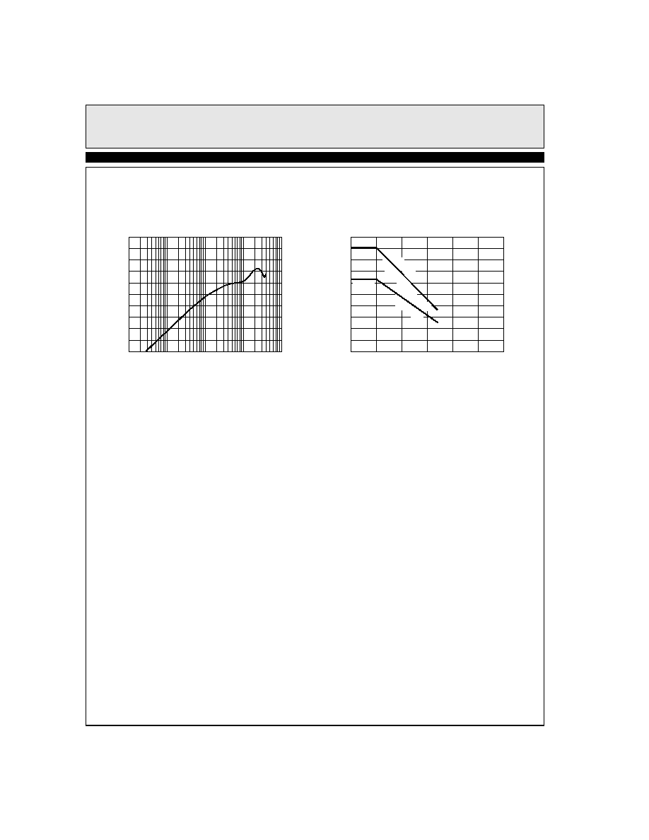
Package Power Dissipation vs Ambient Temp.
JEDEC JESD51-3 Low Effective Thermal Conductivity Test Board
1
0.9
0.8
0.6
0.4
0.2
0
0
50
100
150
Ambient Temperature (∞C)
Po
w
e
r
D
i
s
s
ip
a
t
io
n
(
W
)
0.7
25
75
125
909mW
633mW
0.5
0.3
0.1
SO
16
(0
.15
0")
11
0∞C
/W
QS
OP
16
158
∞C/W

11
EL5393C
Triple 300MHz Current Feedback Amplifier
EL
5393C
Pin Descriptions
EL5393C
SO-16
EL5393C
QSOP-16
Pin Name
Function
Equivalent Circuit
1
1
INA+
Non-inverting input, channel A
Circuit 1
2, 4, 7
2, 4, 7
NC
Not connected (leave disconnected)
3
3
V
S
-
Negative supply
5
5
INB+
Non-inverting input, channel B
(See circuit 1)
6, 11
6, 11
NC
Not connected
8
8
INC+
Non-inverting input, channel C
(See circuit 1)
9
9
INC-
Inverting input, channel C
(See circuit 1)
10
10
OUTC
Output, channel C
Circuit 2
12
12
INB-
Inverting input, channel B
(See circuit 1)
13
13
OUTB
Output, channel B
(See circuit 2)
14
14
V
S
+
Positive supply
15
15
OUTA
Output, channel A
(See circuit 2)
16
16
INA-
Inverting input, channel A
(See circuit 1)
IN-
IN+
V
S
+
V
S
-
V
S
+
V
S
-
OUT

12
EL5393C
Triple 300MHz Current Feedback Amplifier
E
L
5393C
Applications Information
Product Description
The EL5393C is a current-feedback operational ampli-
fier that offers a wide -3dB bandwidth of 300MHz and a
low supply current of 4mA per amplifier. The EL5393C
works with supply voltages ranging from a single 5V to
10V and they are also capable of swinging to within 1V
of either supply on the output. Because of their current-
feedback topology, the EL5393C does not have the nor-
mal gain-bandwidth product associated with voltage-
feedback operational amplifiers. Instead, its -3dB band-
width to remain relatively constant as closed-loop gain is
increased. This combination of high bandwidth and low
power, together with aggressive pricing make the
EL5393C the ideal choice for many low-power/high-
bandwidth applications such as portable, handheld, or
battery-powered equipment.
For varying bandwidth needs, consider the EL5191C
with 1GHz on a 9mA supply current or the EL5192C
with 600MHz on a 6mA supply current. Versions
include single, dual, and triple amp packages with 5-pin
SOT23, 16-pin QSOP, and 8-pin or 16-pin SO outlines.
Power Supply Bypassing and Printed Circuit
Board Layout
As with any high frequency device, good printed circuit
board layout is necessary for optimum performance.
Low impedance ground plane construction is essential.
Surface mount components are recommended, but if
leaded components are used, lead lengths should be as
short as possible. The power supply pins must be well
bypassed to reduce the risk of oscillation. The combina-
tion of a 4.7µ F tantalum capacitor in parallel with a
0.01µ F capacitor has been shown to work well when
placed at each supply pin.
For good AC performance, parasitic capacitance should
be kept to a minimum, especially at the inverting input.
(See the Capacitance at the Inverting Input section) Even
when ground plane construction is used, it should be
removed from the area near the inverting input to mini-
mize any stray capacitance at that node. Carbon or
Metal-Film resistors are acceptable with the Metal-Film
resistors giving slightly less peaking and bandwidth
because of additional series inductance. Use of sockets,
particularly for the SO package, should be avoided if
possible. Sockets add parasitic inductance and capaci-
tance which will result in additional peaking and
overshoot.
Capacitance at the Inverting Input
Any manufacturer's high-speed voltage- or current-
feedback amplifier can be affected by stray capacitance
at the inverting input. For inverting gains, this parasitic
capacitance has little effect because the inverting input is
a virtual ground, but for non-inverting gains, this capac-
itance (in conjunction with the feedback and gain
resistors) creates a pole in the feedback path of the
amplifier. This pole, if low enough in frequency, has the
same destabilizing effect as a zero in the forward open-
loop response. The use of large-value feedback and gain
resistors exacerbates the problem by further lowering
the pole frequency (increasing the possibility of
oscillation.)
The EL5393C has been optimized with a 475
feedback
resistor. With the high bandwidth of these amplifiers,
these resistor values might cause stability problems
when combined with parasitic capacitance, thus ground
plane is not recommended around the inverting input pin
of the amplifier.
Feedback Resistor Values
The EL5393C has been designed and specified at a gain
of +2 with R
F
approximately 500
. This value of feed-
back resistor gives 200MHz of -3dB bandwidth at A
V
=2
with 2dB of peaking. With A
V
=-2, an R
F
of approxi-
mately 500
gives 175MHz of bandwidth with 0.2dB of
peaking. Since the EL5393C is a current-feedback
amplifier, it is also possible to change the value of R
F
to
get more bandwidth. As seen in the curve of Frequency
Response for Various R
F
and R
G
, bandwidth and peak-
ing can be easily modified by varying the value of the
feedback resistor.
Because the EL5393C is a current-feedback amplifier,
its gain-bandwidth product is not a constant for different
closed-loop gains. This feature actually allows the
EL5393C to maintain about the same -3dB bandwidth.
As gain is increased, bandwidth decreases slightly while

13
EL5393C
Triple 300MHz Current Feedback Amplifier
EL
5393C
stability increases. Since the loop stability is improving
with higher closed-loop gains, it becomes possible to
reduce the value of R
F
below the specified 475
and
still retain stability, resulting in only a slight loss of
bandwidth with increased closed-loop gain.
Supply Voltage Range and Single-Supply
Operation
The EL5393C has been designed to operate with supply
voltages having a span of greater than 5V and less than
10V. In practical terms, this means that the EL5393C
will operate on dual supplies ranging from ±2.5V to
±5V. With single-supply, the EL5393C will operate
from 5V to 10V.
As supply voltages continue to decrease, it becomes nec-
essary to provide input and output voltage ranges that
can get as close as possible to the supply voltages. The
EL5393C has an input range which extends to within 2V
of either supply. So, for example, on +5V supplies, the
EL5393C has an input range which spans ±3V. The out-
put range of the EL5393C is also quite large, extending
to within 1V of the supply rail. On a ±5V supply, the
output is therefore capable of swinging from
----
-4V to
+4V. Single-supply output range is larger because of the
increased negative swing due to the external pull-down
resistor to ground.
Video Performance
For good video performance, an amplifier is required to
maintain the same output impedance and the same fre-
quency response as DC levels are changed at the output.
This is especially difficult when driving a standard video
load of 150
, because of the change in output current
with DC level. Previously, good differential gain could
only be achieved by running high idle currents through
the output transistors (to reduce variations in output
impedance.) These currents were typically comparable
to the entire 4mA supply current of each EL5393C
amplifier. Special circuitry has been incorporated in the
EL5393C to reduce the variation of output impedance
with current output. This results in dG and dP specifica-
tions of 0.03% and 0.04∞, while driving 150
at a gain
of 2.
Video performance has also been measured with a 500
load at a gain of +1. Under these conditions, the
EL5393C has dG and dP specifications of 0.03% and
0.04∞.
Output Drive Capability
In spite of its low 4mA of supply current, the EL5393C
is capable of providing a minimum of ±95mA of output
current. With a minimum of ±95mA of output drive, the
EL5393C is capable of driving 50
loads to both rails,
making it an excellent choice for driving isolation trans-
formers in telecommunications applications.
Driving Cables and Capacitive Loads
When used as a cable driver, double termination is
always recommended for reflection-free performance.
For those applications, the back-termination series resis-
tor will decouple the EL5393C from the cable and allow
extensive capacitive drive. However, other applications
may have high capacitive loads without a back-termina-
tion resistor. In these applications, a small series resistor
(usually between 5
and 50
) can be placed in series
with the output to eliminate most peaking. The gain
resistor (R
G
) can then be chosen to make up for any gain
loss which may be created by this additional resistor at
the output. In many cases it is also possible to simply
increase the value of the feedback resistor (R
F
) to reduce
the peaking.
Current Limiting
The EL5393C has no internal current-limiting circuitry.
If the output is shorted, it is possible to exceed the Abso-
lute Maximum Rating for output current or power
dissipation, potentially resulting in the destruction of the
device.
Power Dissipation
With the high output drive capability of the EL5393C, it
is possible to exceed the 125∞C Absolute Maximum
junction temperature under certain very high load cur-
rent conditions. Generally speaking when R
L
falls below
about 25
, it is important to calculate the maximum
junction temperature (T
JMAX
) for the application to
determine if power supply voltages, load conditions, or
package type need to be modified for the EL5393C to

14
EL5393C
Triple 300MHz Current Feedback Amplifier
E
L
5393C
remain in the safe operating area. These parameters are
calculated as follows:
where:
7
0$;
0D[LPXP $PELHQW 7HPSHUDWXUH
-$
7KHUPDO 5HVLVWDQFH RI WKH 3DFNDJH
Q 1XPEHU RI $PSOLILHUV LQ WKH 3DFNDJH
3'
0$;
0D[LPXP 3RZHU 'LVVLSDWLRQ RI (DFK
$PSOLILHU LQ WKH 3DFNDJH
PD
MAX
for each amplifier can be calculated as follows:
where:
9
6
6XSSO\ 9ROWDJH
,
60$;
0D[LPXP 6XSSO\ &XUUHQW RI $
9
2870$;
0D[LPXP 2XWSXW 9ROWDJH 5HTXLUHG�
5
/
/RDG 5HVLVWDQFH
T
JMA X
T
MA X
JA
n
PD
MA X
◊
◊
(
)
+
=
PD
MA X
2
(
V
S
I
SMA X
)
V
S
(
V
OU T MAX
)
V
OU T MAX
R
L
----------------------------
◊
≠
+
◊
◊
=
15
EL5393C
Triple 300MHz Current Feedback Amplifier
E
L
5393C
General Disclaimer
Specifications contained in this data sheet are in effect as of the publication date shown. Elantec, Inc. reserves the right to make changes in the cir-
cuitry or specifications contained herein at any time without notice. Elantec, Inc. assumes no responsibility for the use of any circuits described
herein and makes no representations that they are free from patent infringement.
WARNING - Life Support Policy
Elantec, Inc. products are not authorized for and should not be used
within Life Support Systems without the specific written consent of
Elantec, Inc. Life Support systems are equipment intended to sup-
port or sustain life and whose failure to perform when properly used
in accordance with instructions provided can be reasonably
expected to result in significant personal injury or death. Users con-
templating application of Elantec, Inc. Products in Life Support
Systems are requested to contact Elantec, Inc. factory headquarters
to establish suitable terms & conditions for these applications. Elan-
tec, Inc.'s warranty is limited to replacement of defective
components and does not cover injury to persons or property or
other consequential damages.
April 26, 2
001
Printed in U.S.A.
Elantec Semiconductor, Inc.
675 Trade Zone Blvd.
Milpitas, CA 95035
Telephone: (408) 945-1323
(888) ELANTEC
Fax:
(408) 945-9305
European Office: +44-118-977-6020
Japan Technical Center: +81-45-682-5820