 | –≠–ª–µ–∫—Ç—Ä–æ–Ω–Ω—ã–π –∫–æ–º–ø–æ–Ω–µ–Ω—Ç: EL5396CU | –°–∫–∞—á–∞—Ç—å:  PDF PDF  ZIP ZIP |
Note: All information contained in this data sheet has been carefully checked and is believed to be accurate as of the date of publication; however, this data sheet cannot be a "controlled document". Current revisions, if any, to these
specifications are maintained at the factory and are available upon your request. We recommend checking the revision level before finalization of your design documentation.
© 2001 Elantec Semiconductor, Inc.
E
L
5
3
9
6
C
-
P
r
e
l
i
m
i
n
a
r
y
General Description
The EL5396C is a triple channel, fixed gain amplifier with a band-
width of 400MHz, making these amplifiers ideal for today's high
speed video and monitor applications. The EL5396C features internal
gain setting resistors and can be configured in a gain of +1, -1 or +2.
The same bandwidth is seen in both gain-of-1 and gain-of-2
applications.
The EL5396C can be run from a single or dual supply voltage of 5V to
10V and consumes just 9mA of supply current per channel. Each
channel of the EL5396C has a disable. Upon being disabled, the out-
puts are tri-stated and the power supply current reduces to less than
150µA per amplifier. Allowing the CE pin to float, or applying a low
logic level will enable the amplifier.
For applications where board space is critical, the EL5396C is offered
in the 16-pin QSOP package, as well as a 16-pin SO. The EL5396C is
specified for operation over the full industrial temperature range of
---
-40
∞
C to +85
∞
C.
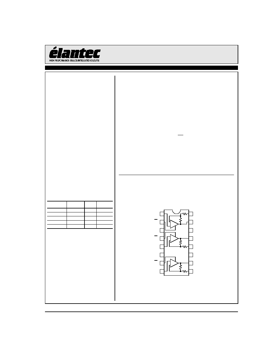
Pin Configurations
1
2
3
4
16
15
14
13
5
6
7
12
11
10
8
9
EL5396CS, EL5396CU
INA-
OUTA
VS+
OUTB
INB-
NC
OUTC
INC-
INA+
CEA
VS-
CEB
INB+
NC
CEC
INC+
16-Pin SO & QSOP
-
+
-
+
-
+
Features
∑ Gain selectable (+1, -1, +2)
∑ 400MHz -3dB Bandwidth (A
V
= 1,
2)
∑ 9mA supply current (per amplifier)
∑ Single and dual supply operation,
from 5V to 10V
∑ Power-down
∑ Available in 16-pin QSOP package
∑ Single (EL5196C) available
∑ 200MHz, 3mA product available
(EL5197C, EL5397C)
Applications
∑ Video Amplifiers
∑ Cable Drivers
∑ RGB Amplifiers
∑ Test Equipment
∑ Instrumentation
∑ Current to Voltage Converters
Ordering Information
Part No
Package
Tape &
Reel
Outline #
EL5396CS
16-Pin SO
-
MDP0027
EL5396CS-T7
16-Pin SO
7"
MDP0027
EL5396CS-T13
16-Pin SO
13"
MDP0027
EL5396CU
16-Pin QSOP
-
MDP0040
EL5396CU-T13
16-Pin QSOP
13"
MDP0040
EL5396C - Preliminary
Triple 400MHz Fixed Gain Amplifier
S
e
p
t
e
m
b
e
r
1
9
,
2
0
0
1
2
EL5396C - Preliminary
Triple 400MHz Fixed Gain Amplifier
E
L
5
3
9
6
C
-
P
r
e
l
i
m
i
n
a
r
y
Absolute Maximum Ratings
(T
A
= 25∞C)
Values beyond absolute maximum ratings can cause the device to be pre-
maturely damaged. Absolute maximum ratings are stress ratings only
and functional device operation is not implied.
Supply Voltage between V
S
+ and V
S
-
11V
Maximum Continuous Output Current
50mA
Operating Junction Temperature
125∞C
Power Dissipation
See Curves
Pin Voltages
V
S
- - 0.5V to V
S
+ +0.5V
Storage Temperature
-65∞C to +150∞C
Operating Temperature
-40∞C to +85∞C
Lead Temperature
260∞C
Important Note:
All parameters having Min/Max specifications are guaranteed. Typ values are for information purposes only. Unless otherwise noted, all tests are at the
specified temperature and are pulsed tests, therefore: T
J
= T
C
= T
A
.
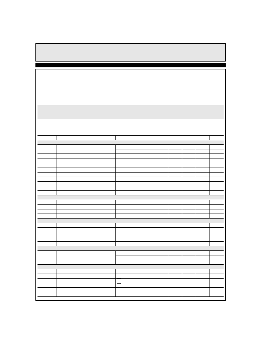
Electrical Characteristics
V
S
+ = +5V, V
S
- = -5V, R
L
= 150
, T
A
= 25∞C unless otherwise specified.
Parameter
Description
Conditions
Min
Typ
Max
Unit
AC Performance
BW
-3dB Bandwidth
A
V
= +1
400
MHz
A
V
= +2
400
MHz
BW1
0.1dB Bandwidth
35
MHz
SR
Slew Rate
V
O
= -2.5V to +2.5V, A
V
= +2
TBD
-2600
V/µs
ts
0.1% Settling Time
V
OUT
= -2.5V to +2.5V, AV = -1
9
ns
C
S
Channel Separation
f = 5MHz
68
dB
e
n
Input Voltage Noise
3.8
nV/
Hz
i
n
-
IN- input current noise
25
pA/
Hz
i
n
+
IN+ input current noise
55
pA/
Hz
dG
Differential Gain Error
[1]
A
V
= +2
0.035
%
dP
Differential Phase Error
[1]
A
V
= +2
0.04
∞
DC Performance
V
OS
Offset Voltage
-15
1
15
mV
T
C
V
OS
Input Offset Voltage Temperature Coefficient
Measured from T
MIN
to T
MAX
5
µV/∞C
A
E
Gain Error
V
O
= -3V to +3V
-2
1.3
2
%
R
F
, R
G
Internal R
F
and R
G
320
400
480
Input Characteristics
CMIR
Common Mode Input Range
±3V
±3.3V
V
+I
IN
+ Input Current
-120
40
120
µA
-I
IN
- Input Current
-40
4
40
µA
R
IN
Input Resistance
27
k
C
IN
Input Capacitance
0.5
pF
Output Characteristics
V
O
Output Voltage Swing
R
L
= 150
to GND
±3.4V
±3.7V
V
R
L
= 1K
to GND
±3.8V
±4.0V
V
I
OUT
Output Current
R
L
= 10
to GND
95
120
mA
Enable (selected packages only)
t
EN
Enable Time
40
ns
t
DIS
Disable Time
TBD
ns
I
IHCE
CE pin Input High Current
CE = V
S
+
0.8
6
µA
I
ILCE
CE pin Input Low Current
CE = V
S
-
0
-0.1
µA
V
IHCE
CE pin Input High Voltage for Power Down
V
S
+ -0.5
V
V
ILCE
CE pin Input Low Voltage for Power Up
V
S
+ -3
V
3
EL5396C - Preliminary
Triple 400MHz Fixed Gain Amplifier
E
L
5
3
9
6
C
-
P
r
e
l
i
m
i
n
a
r
y
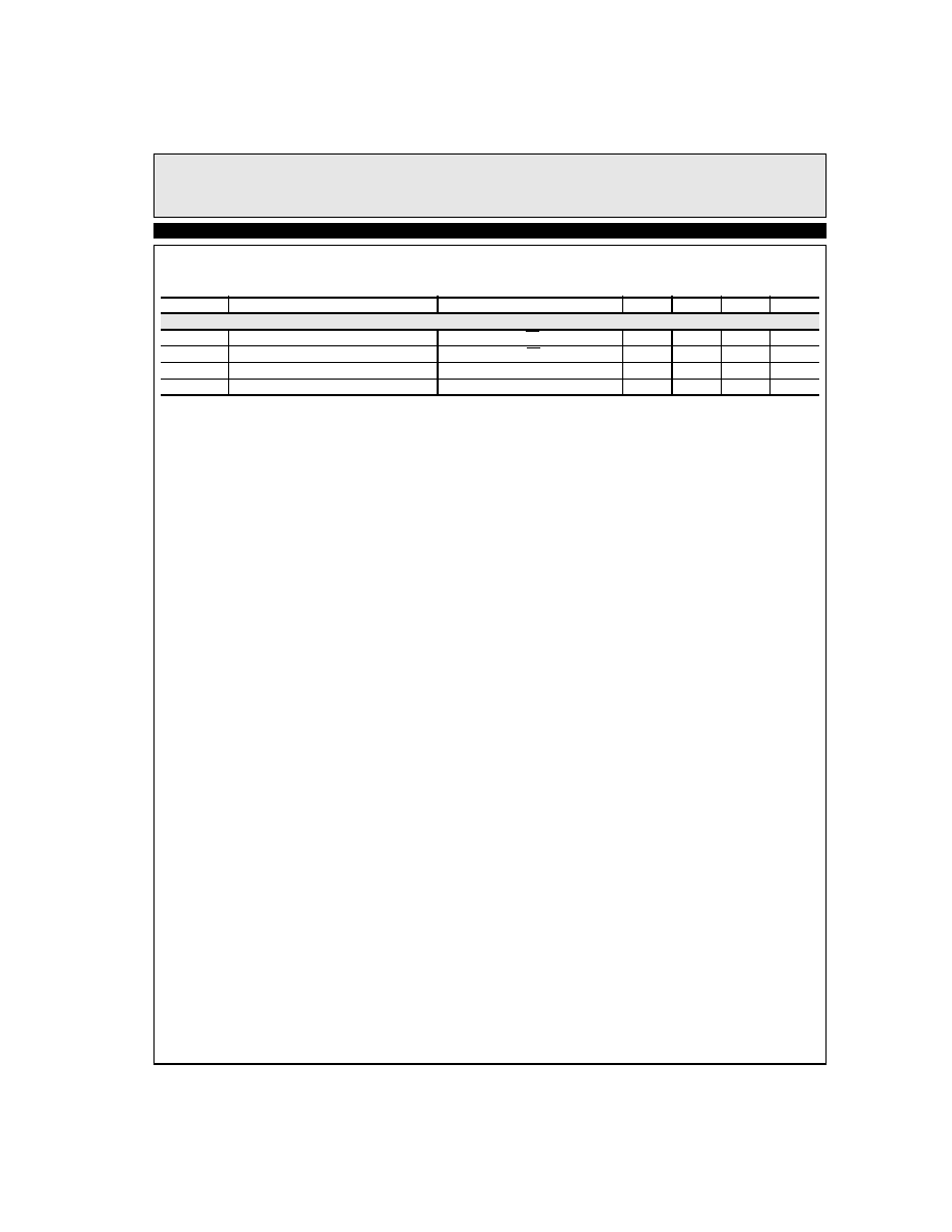
Supply
Is
ON
Supply Current - Enabled (per amplifier)
No Load, V
IN
= 0V, CE = -5V
8
9
10.5
mA
Is
OFF
Supply Current - Disabled (per amplifier)
No Load, V
IN
= 0V, CE = +4.5V
95
130
µA
PSRR
Power Supply Rejection Ratio
DC, V
S
= ±4.75V to ±5.25V
55
75
dB
-IPSR
- Input Current Power Supply Rejection
DC, V
S
= ±4.75V to ±5.25V
-2
2
µA/V
1. Standard NTSC test, AC signal amplitude = 286mV
P-P
, f = 3.58MHz
Electrical Characteristics
V
S
+ = +5V, V
S
- = -5V, R
L
= 150
, T
A
= 25∞C unless otherwise specified.
Parameter
Description
Conditions
Min
Typ
Max
Unit
4
EL5396C - Preliminary
Triple 400MHz Fixed Gain Amplifier
E
L
5
3
9
6
C
-
P
r
e
l
i
m
i
n
a
r
y
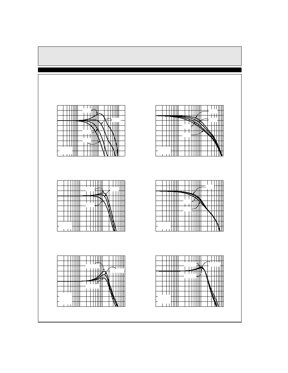
Typical Performance Curves
Non-Inverting Frequency Response (Gain)
1M
10M
100M
1G
6
2
-2
-6
-10
-14
Frequency (Hz)
N
o
r
m
a
l
i
z
e
d
M
a
g
n
i
t
u
d
e
(
d
B
)
A
V
=2
A
V
=5
A
V
=10
A
V
=1
R
F
=750
R
L
=150
Non-Inverting Frequency Response (Phase)
1M
10M
100M
1G
90
0
-90
-180
-270
-360
Frequency (Hz)
P
h
a
s
e
(
∞
)
A
V
=2
A
V
=5
A
V
=10
A
V
=1
R
F
=750
R
L
=150
Inverting Frequency Response (Gain)
1M
10M
100M
1G
6
2
-2
-6
-10
-14
Frequency (Hz)
N
o
r
m
a
l
i
z
e
d
M
a
g
n
i
t
u
d
e
(
d
B
)
A
V
=-2
A
V
=-3
A
V
=-1
R
F
=500
R
L
=150
Inverting Frequency Response (Phase)
1M
10M
100M
1G
90
0
-90
-180
-270
-360
Frequency (Hz)
P
h
a
s
e
(
∞
)
A
V
=-2
A
V
=-3
A
V
=-1
R
F
=500
R
L
=150
Frequency Response for Various R
L
1M
10M
100M
1G
6
2
-2
-6
-10
-14
Frequency (Hz)
N
o
r
m
a
l
i
z
e
d
M
a
g
n
i
t
u
d
e
(
d
B
)
A
V
=2
R
F
=500
R
L
=100
R
L
=500
R
L
=150
Frequency Response for Various C
IN
-
1M
10M
100M
1G
10
6
2
-2
-6
-10
Frequency (Hz)
N
o
r
m
a
l
i
z
e
d
M
a
g
n
i
t
u
d
e
(
d
B
)
A
V
=2
R
F
=500
R
L
=150
0pF added
2pF added
1pF added

5
EL5396C - Preliminary
Triple 400MHz Fixed Gain Amplifier
E
L
5
3
9
6
C
-
P
r
e
l
i
m
i
n
a
r
y
Typical Performance Curves
Frequency Response for Various C
L
1M
10M
100M
1G
14
10
6
2
-2
-6
Frequency (Hz)
N
o
r
m
a
l
i
z
e
d
M
a
g
n
i
t
u
d
e
(
d
B
)
A
V
=2
R
L
=150
R
F
=R
G
=500
33pF
22pF
15pF
8pF
0pF
Group Delay vs Frequency
1M
10M
100M
1G
Frequency (Hz)
D
e
l
a
y
(
n
s
)
A
V
=1
R
F
=750
A
V
=2
R
F
=500
Frequency Response for Various Common-mode Input
Voltages
1M
10M
100M
1G
6
2
-2
-6
-10
-14
Frequency (Hz)
N
o
r
m
a
l
i
z
e
d
M
a
g
n
i
t
u
d
e
(
d
B
)
A
V
=2
R
F
=500
R
L
=150
V
CM
=3V
V
CM
=0V
V
CM
=-3V
3.5
0
3
2.5
2
1.5
1
0.5
Frequency Response for Various R
F
1M
10M
100M
1G
6
2
-2
-6
-10
-14
Frequency (Hz)
N
o
r
m
a
l
i
z
e
d
M
a
g
n
i
t
u
d
e
(
d
B
)
A
V
=2
R
G
=R
F
R
L
=150
340
475
620
750
1.2k
Transimpedance (ROL) vs Frequency
1k
Frequency (Hz)
10k
100k
1M
10M
100
1G
10M
100
1k
10k
100k
1M
Phase
Gain
PSRR and CMRR vs Frequency
P
S
R
R
/
C
M
R
R
(
d
B
)
Frequency (Hz)
PSRR+
PSRR-
CMRR
M
a
g
n
i
t
u
d
e
(
)
20
-80
-60
-40
-20
0
10k
100k
1M
10M
1G
100M
-90
-180
-270
-360
0
P
h
a
s
e
(
∞
)

6
EL5396C - Preliminary
Triple 400MHz Fixed Gain Amplifier
E
L
5
3
9
6
C
-
P
r
e
l
i
m
i
n
a
r
y
Typical Performance Curves
-3dB Bandwidth vs Supply Voltage for Non-inverting Gains
5
6
9
10
400
200
150
100
50
0
Total Supply Voltage (V)
-
3
d
B
B
a
n
d
w
i
d
t
h
(
M
H
z
)
A
V
=2
A
V
=5
A
V
=10
A
V
=1
R
F
=750
R
L
=150
Peaking vs Supply Voltage for Non-inverting Gains
4
3.5
2
1
0.5
0
Total Supply Voltage (V)
P
e
a
k
i
n
g
(
d
B
)
A
V
=2
A
V
=1
R
F
=750
R
L
=150
-3dB Bandwidth vs Supply Voltage for Inverting Gains
250
200
150
100
0
Total Supply Voltage (V)
-
3
d
B
B
a
n
d
w
i
d
t
h
(
M
H
z
)
A
V
=-2
A
V
=-5
A
V
=-1
R
F
=500
R
L
=150
350
7
8
5
6
9
10
7
8
5
6
9
10
7
8
300
250
50
A
V
=10
2.5
1.5
3
Peaking vs Supply Voltage for Inverting Gains
2.5
2
1.5
1
0.5
0
Total Supply Voltage (V)
P
e
a
k
i
n
g
(
d
B
)
A
V
=-2
A
V
=-1
R
F
=500
R
L
=150
5
6
9
10
7
8
Non-inverting Frequency Response (Gain)
1M
10M
100M
1G
Frequency (Hz)
N
o
r
m
a
l
i
z
e
d
M
a
g
n
i
t
u
d
e
(
d
B
)
6
2
-2
-6
-10
-14
Non-inverting Frequency Response (Phase)
1M
10M
100M
1G
Frequency (Hz)
P
h
a
s
e
(
∞
)
90
0
-90
-180
-270
-360
R
F
=750
R
L
=150
A
V
=1
A
V
=2
A
V
=5
A
V
=10
R
F
=750
R
L
=150
A
V
=1
A
V
=2
A
V
=5
A
V
=10
7
EL5396C - Preliminary
Triple 400MHz Fixed Gain Amplifier
E
L
5
3
9
6
C
-
P
r
e
l
i
m
i
n
a
r
y
Typical Performance Curves
Inverting Frequency Response (Gain)
1M
10M
100M
1G
Frequency (Hz)
N
o
r
m
a
l
i
z
e
d
M
a
g
n
i
t
u
d
e
(
d
B
)
6
2
-2
-6
-10
-14
R
F
=500
R
L
=150
A
V
=-1
A
V
=-2
A
V
=-5
Inverting Frequency Response (Phase)
1M
10M
100M
1G
Frequency (Hz)
P
h
a
s
e
(
∞
)
90
0
-90
-180
-270
-360
R
F
=500
R
L
=150
A
V
=-1
A
V
=-2
A
V
=-5
-3dB Bandwidth vs Temperature for Inverting Gains
250
200
150
50
0
-40
10
110
160
Ambient Temperature (∞C)
-
3
d
B
B
a
n
d
w
i
d
t
h
(
M
H
z
)
100
60
Peaking vs Temperature
2.5
2
1.5
0.5
0
-0.5
-40
10
110
160
Ambient Temperature (∞C)
P
e
a
k
i
n
g
(
d
B
)
1
60
-3dB Bandwidth vs Temperature for Non-inverting Gains
500
400
300
100
0
-40
10
110
160
Ambient Temperature (∞C)
-
3
d
B
B
a
n
d
w
i
d
t
h
(
M
H
z
)
200
60
A
V
=1
A
V
=2
A
V
=5
A
V
=10
R
F
=750
R
L
=150
A
V
=-1
A
V
=-2
A
V
=-5
R
F
=500
R
L
=150
R
L
=150
A
V
=1
A
V
=-1
Voltage and Current Noise vs Frequency
100
Frequency ()
1000
10k
100k
10M
1M
i
n
+
i
n
-
e
n
V
o
l
t
a
g
e
N
o
i
s
e
(
n
V
/
H
z
)
,
C
u
r
r
e
n
t
N
o
i
s
e
(
p
A
/
H
z
)
1000
1
10
100

8
EL5396C - Preliminary
Triple 400MHz Fixed Gain Amplifier
E
L
5
3
9
6
C
-
P
r
e
l
i
m
i
n
a
r
y
Typical Performance Curves
Closed Loop Output Impedance vs Frequency
Frequency (Hz)
O
u
t
p
u
t
I
m
p
e
d
a
n
c
e
(
)
100
0.001
0.1
10
0.01
1
S
u
p
p
l
y
C
u
r
r
e
n
t
(
m
A
)
10
0
4
8
2
6
0
Supply Voltage (V)
Supply Current vs Supply Voltage
12
2
10
8
6
4
100
1k
100M
1G
1M
100k
10M
10k
10
Frequency (MHz)
100
I
n
p
u
t
P
o
w
e
r
I
n
t
e
r
c
e
p
t
(
d
B
m
)
25
-10
15
20
-5
0
5
10
A
V
=+2
R
L
=150
Two-tone 3rd Order
Input Referred Intermodulation Intercept (IIP3)
A
V
=+2
R
L
=100
2nd and 3rd Harmonic Distortion vs Frequency
1
Frequency (MHz)
10
100
H
a
r
m
o
n
i
c
D
i
s
t
o
r
t
i
o
n
(
d
B
c
)
-20
-90
-70
-30
-50
-80
-40
-60
A
V
=+2
V
OUT
=2V
P-P
R
L
=100
2nd Order
Distortion
3rd Order
Distortion
0.03
0.02
0.01
0
-0.01
-0.02
-0.03
-0.04
-0.05
d
G
(
%
)
o
r
d
P
(
∞
)
-1
-0.5
0
0.5
1
dP
dG
A
V
=2
R
F
=R
G
=500
R
L
=150
Differential Gain/Phase vs DC Input
Voltage at 3.58MHz
DC Input Voltage
0.04
0.03
0.02
0.01
0
-0.01
-0.02
-0.03
-0.04
d
G
(
%
)
o
r
d
P
(
∞
)
-1
-0.5
0
0.5
1
dP
dG
A
V
=1
R
F
=750
R
L
=500
Differential Gain/Phase vs DC Input
Voltage at 3.58MHz
DC Input Voltage
9
EL5396C - Preliminary
Triple 400MHz Fixed Gain Amplifier
E
L
5
3
9
6
C
-
P
r
e
l
i
m
i
n
a
r
y
Typical Performance Curves
Output Voltage Swing vs Frequency
THD<1%
1
Frequency (MHz)
10
100
O
u
t
p
u
t
V
o
l
t
a
g
e
S
w
i
n
g
(
V
P
P
)
10
0
2
4
6
8
R
L
=150
R
L
=500
1
Frequency (MHz)
10
100
O
u
t
p
u
t
V
o
l
t
a
g
e
S
w
i
n
g
(
V
P
P
)
10
0
2
4
6
8
Output Voltage Swing vs Frequency
THD<0.1%
R
L
=150
R
L
=500
A
V
=2
A
V
=2
Small Signal Step Response
Large Signal Step Response
Settling Time vs Settling Accuracy
25
20
15
10
0
S
e
t
t
l
i
n
g
T
i
m
e
(
n
s
)
0.01
0.1
1
Settling Accuracy (%)
5
A
V
=2
R
F
=R
G
=500
R
L
=150
V
STEP
=5V
P-P
output
200mV/div
10ns/div
1V/div
10ns/div
V
S
=±5V
R
L
=150
A
V
=2
R
F
=R
G
=500
V
S
=±5V
R
L
=150
A
V
=2
R
F
=R
G
=500
Transimpedance (RoI) vs Temperature
625
600
575
550
525
-40
10
60
110
160
Die Temperature (∞C)
R
o
I
(
k
)

10
EL5396C - Preliminary
Triple 400MHz Fixed Gain Amplifier
E
L
5
3
9
6
C
-
P
r
e
l
i
m
i
n
a
r
y
Typical Performance Curves
PSRR and CMRR vs Temperature
90
70
50
40
30
20
10
-40
10
60
110
160
Die Temperature (∞C)
P
S
R
R
/
C
M
R
R
(
d
B
)
60
80
PSRR
CMRR
ICMR and IPSR vs Temperature
2
1.5
0.5
0
-0.5
-40
10
60
110
160
Die Temperature (∞C)
I
C
M
R
/
I
P
S
R
(
µ
A
/
V
)
1
ICMR+
IPSR
ICMR-
Offset Voltage vs Temperature
2
1
0
-1
-2
-40
10
60
110
160
Die Temperature (∞C)
V
O
S
(
m
V
)
Input Current vs Temperature
60
40
20
-20
-40
-60
-40
10
110
160
Temperature (∞C)
I
n
p
u
t
C
u
r
r
e
n
t
(
µ
A
)
0
60
Positive Input Resistance vs Temperature
60
50
30
20
10
0
-40
10
110
160
Temperature (∞C)
R
I
N
+
(
k
)
40
60
IB-
IB+
Supply Current vs Temperature
5
3
2
1
0
-40
10
110
160
Temperature (∞C)
S
u
p
p
l
y
C
u
r
r
e
n
t
(
m
A
)
4
60
11
EL5396C - Preliminary
Triple 400MHz Fixed Gain Amplifier
E
L
5
3
9
6
C
-
P
r
e
l
i
m
i
n
a
r
y
Typical Performance Curves
Negative Output Swing vs Temperature for Various Loads
-3.5
-3.6
-3.7
-3.9
-4
-4.1
-4.2
-40
10
110
160
Temperature (∞C)
V
O
U
T
(
V
)
-3.8
60
Positive Output Swing vs Temperature for Various Loads
4.2
4.1
4
3.8
3.7
3.6
3.5
-40
10
110
160
Temperature (∞C)
V
O
U
T
(
V
)
3.9
60
1k
150
1k
150
Slew Rate vs Temperature
4000
3500
3000
2500
-40
10
60
110
160
Die Temperature (∞C)
S
l
e
w
R
a
t
e
(
V
/
µ
S
)
Output Current vs Temperature
130
125
120
115
-40
10
60
110
160
Die Temperature (∞C)
I
O
U
T
(
m
A
)
A
V
=2
R
F
=R
G
=500
R
L
=150
Sink
Source
Channel-to-Channel Isolation vs Frequency
100k
1M
10M
100M
Frequency (Hz)
G
a
i
n
(
d
B
)
0
-20
-40
-60
-80
-100
400M
Package Power Dissipation vs Ambient Temp.
JEDEC JESD51-3 Low Effective Thermal Conductivity Test Board
1
0.9
0.8
0.6
0.4
0.2
0
0
50
100
150
Ambient Temperature (∞C)
P
o
w
e
r
D
i
s
s
i
p
a
t
i
o
n
(
W
)
0.7
25
75
125
909mW
633mW
0.5
0.3
0.1
SO
16
110
∞C/W
QSO
P16
158∞
C/W

12
EL5396C - Preliminary
Triple 400MHz Fixed Gain Amplifier
E
L
5
3
9
6
C
-
P
r
e
l
i
m
i
n
a
r
y
Pin Descriptions
EL5396C
16-Pin SO & 16-
Pin QSOP
Pin Name
Function
Equivalent Circuit
1
INA+
Non-inverting input, Channel A
Circuit1
2
CEA
Amplifier A enable
Circuit 2
3
VS-
Negative supply
4
CEB
Amplifier B enable
(Reference Circuit 2)
5
INB+
Non-inverting input, Channel B
(Reference Circuit 1)
6
NC
Not connected
7
CEC
Amplifier C enable
(Reference Circuit 2)
8
INC+
Non-inverting input, Channel C
(Reference Circuit 1)
9
INC-
Inverting input, Channel C
(Reference Circuit 1)
10
OUTC
Output, Channel C
Circuit 3
11
NC
Not connected
12
INB-
Inverting input, Channel B
(Reference Circuit 1)
13
OUTB
Output, Channel B
(Reference Circuit 3)
14
VS+
Positive supply
15
OUTA
Output, Channel A
(Reference Circuit 3)
16
INA-
Inverting input, Channel A
(Reference Circuit 1)
R
G
R
F
IN-
IN+
CE
R
F
OUT

13
EL5396C - Preliminary
Triple 400MHz Fixed Gain Amplifier
E
L
5
3
9
6
C
-
P
r
e
l
i
m
i
n
a
r
y
General Disclaimer
Specifications contained in this data sheet are in effect as of the publication date shown. Elantec, Inc. reserves the right to make changes in the cir-
cuitry or specifications contained herein at any time without notice. Elantec, Inc. assumes no responsibility for the use of any circuits described
herein and makes no representations that they are free from patent infringement.
WARNING - Life Support Policy
Elantec, Inc. products are not authorized for and should not be used
within Life Support Systems without the specific written consent of
Elantec, Inc. Life Support systems are equipment intended to sup-
port or sustain life and whose failure to perform when properly used
in accordance with instructions provided can be reasonably
expected to result in significant personal injury or death. Users con-
templating application of Elantec, Inc. Products in Life Support
Systems are requested to contact Elantec, Inc. factory headquarters
to establish suitable terms & conditions for these applications. Elan-
tec, Inc.'s warranty is limited to replacement of defective
components and does not cover injury to persons or property or
other consequential damages.
S
e
p
t
e
m
b
e
r
1
9
,
2
0
0
1
Printed in U.S.A.
Elantec Semiconductor, Inc.
675 Trade Zone Blvd.
Milpitas, CA 95035
Telephone: (408) 945-1323
(888) ELANTEC
Fax:
(408) 945-9305
European Office: +44-118-977-6020
Japan Technical Center: +81-45-682-5820