 | –≠–ª–µ–∫—Ç—Ä–æ–Ω–Ω—ã–π –∫–æ–º–ø–æ–Ω–µ–Ω—Ç: EL5444CN | –°–∫–∞—á–∞—Ç—å:  PDF PDF  ZIP ZIP |

© 1998 Elantec, Inc.
EL
5144C, EL5146
C
,
E
L
5244C, EL
5246C, EL5444C
General Description
The EL5144C series amplifiers are voltage feedback, high speed, rail
to rail amplifiers designed to operate on a single +5V supply. They
offer unity gain stability with an unloaded ≠3dB bandwidth of 100
MHz. The input common mode voltage range extends from the nega-
tive rail to within 1.5V of the positive rail. Driving a 75
double
terminated coaxial cable, the EL5144C series amplifiers drive to
within 150 mV of either rail. The 200 V/
µ
sec slew rate and 0.1% / 0.1
∞
differential gain / differential phase makes these parts ideal for com-
posite and component video applications. With its voltage feedback
architecture, this amplifier can accept reactive feedback networks,
allowing them to be used in analog filtering applications These ampli-
fiers will source 90 mA and sink 65 mA.
The EL5146C and EL5246C have a power-savings disable feature.
Applying a standard TTL low logic level to the CE (Chip Enable) pin
reduces the supply current to 2.6
µ
A within 10 nsec. Turn on time is
500 nsec, allowing true break-before-make conditions for multiplex-
ing applications. Allowing the CE pin to float or applying a high logic
level will enable the amplifier.
For applications where board space is critical, singles are offered in a
SOT23-5 package, duals in MSOP-8 and MSOP-10 packages, and
quads in a QSOP-16 package. Singles, duals and quads are also avail-
able in industry standard pinouts in SOIC and PDIP packages. All
parts operate over the industrial temperature range of -40
∞
C to +85
∞
C.
OUT
GND
V
S
IN-
IN+
SOT23-5
1
2
3
5
4
-
+
EL5144C
Dual and Quad Amplifier Pin Configurations on Page 12
Pin Configurations
1
2
3
4
8
7
6
5
-
+
IN-
IN+
GND
NC
OUT
V
S
NC
CE
SOIC-8, PDIP-8
EL5146C
Features
∑ Rail to Rail Output Swing
∑ -3 dB Bandwidth = 100 MHz
∑ Single Supply +5V operation
∑ Power Down to 2.6 µA
∑ Large Input Common Mode Range
0V < V
CM
< 3.5 V
∑ Diff Gain/Phase = 0.1%/0.1∞
∑ Low Power 35mW per amplifier
∑ Space Saving SOT23-5, MSOP-
8&10, & QSOP-16 packaging
Applications
∑ Video Amplifier
∑ 5 Volt Analog Signal Processing
∑ Multiplexer
∑ Line Driver
∑ Portable Computers
∑ High Speed Communications
∑ Sample & Hold Amplifier
∑ Comparator
Ordering Information
Part No
Temp. Range
Package
Outline #
EL5144CW
-40∞C to +85∞C
5 Pin SOT23
MDP0038
EL5146CN
-40∞C to +85∞C
8 Pin PDIP
MDP0031
EL5146CS
-40∞C to +85∞C
8 Pin SOIC
MDP0027
EL5244CN
-40∞C to +85∞C
8 Pin PDIP
MDP0031
EL5244CS
-40∞C to +85∞C
8 Pin SOIC
MDP0027
EL5244CY
-40∞C to +85∞C
8 Pin MSOP
MDP0043
EL5246CN
-40∞C to +85∞C
14 Pin PDIP
MDP0031
EL5246CS
-40∞C to +85∞C
14 Pin SOIC
MDP0027
EL5246CY
-40∞C to +85∞C
10 Pin MSOP
MDP0043
EL5444CN
-40∞C to +85∞C
14 Pin PDIP
MDP0031
EL5444CS
-40∞C to +85∞C
14 Pin SOIC
MDP0027
EL5444CU
-40∞C to +85∞C
16 Pin QSOP
MDP0040
0V
5V
EL5144C, EL5146C, EL5244C,
EL5246C, EL5444C
100 MHz Single Supply Rail to Rail Amplifier
Marc
h
1, 2000

2
EL5144C, EL5146C, EL5244C, EL5246C,
EL5444C
100 MHz Single Supply Rail to Rail Amplifier
EL514
4C
, E
L
5146C, EL
5244C, EL5246C, E
L
5444C
Absolute Maximum Ratings
(T
A
= 25 ∞C)
Values beyond absolute maximum ratings can cause the device to be pre-
maturely damaged. Absolute maximum ratings are stress ratings only and
functional device operation is not implied.
Supply Voltage between V
S
and GND
+6V
Maximum Continuous Output Current
50mA
Power Dissipation
See Curves
Pin Voltages
GND - 0.5V to V
S
+0.5V
Storage Temperature
-65∞C to +150∞C
Operating Temperature
-40∞C to +85∞C
Lead Temperature
260∞C
Important Note:
All parameters having Min/Max specifications are guaranteed. Typ values are for information purposes only. Unless otherwise noted, all tests are at the specified
temperature and are pulsed tests, therefore: T
J
= T
C
= T
A
.
Electrical Characteristics
V
S
=+5V, GND=0V, T
A
=25∞C, CE = +2V, unless otherwise specified.
Parameter
Description
Conditions
Min
Typ
Max
Units
AC Performance
dG
Differential Gain Error
[1]
G=2, R
L
=150
to 2.5V, R
F
=1K
0.1
%
dP
Differential Phase Error
[1]
G=2, R
L
=150
to 2.5V, R
F
=1K
0.1
deg
BW
Bandwidth
-3dB, G=1, R
L
=10k
,
R
F
=0
100
MHz
-3dB, G=1, R
L
=150
,
R
F
=0
60
MHz
BW1
Bandwidth
±0.1dB, G=1, R
L
=150
to GND, R
F
=0
8
MHz
GBWP
Gain Bandwidth Product
60
MHz
SR
Slew Rate
G=1, R
L
=150
to GND, R
F
=0, V
O
=0.5V to
3.5V
150
200
V/µs
ts
Settling Time
to 0.1%, V
OUT
= 0 to 3V
35
ns
DC Performance
A
VOL
Open Loop Voltage Gain
R
L
=no load, V
OUT
=0.5V to 3V
54
65
dB
R
L
=150
to GND, V
OUT
=0.5V to 3V
40
50
dB
V
OS
Offset Voltage
V
CM
=1V, SOT23-5 and MSOP packages
25
mV
V
CM
=1V, All other packages
15
mV
T
C
V
OS
Input Offset Voltage Temperature Coefficient
10
µ
V/
O
C
I
B
Input Bias Current
V
CM
=0V & 3.5V
2
100
nA
Input Characteristics
CMIR
Common Mode Input Range
CMRR
47dB
0
3.5
V
CMRR
Common Mode Rejection Ratio
DC, V
CM
= 0 to 3.0V
50
60
dB
DC, V
CM
= 0 to 3.5V
47
60
dB
R
IN
Input Resistance
1.5
G
C
IN
Input Capacitance
1.5
pF
Output Characteristics
V
OP
Positive Output Voltage Swing
R
L
=150
to 2.5V
[2]
4.70
4.85
V
R
L
=150
to GND
[2]
4.20
4.65
V
R
L
=1K
to 2.5V
[2]
4.95
4.97
V
V
ON
Negative Output Voltage Swing
R
L
=150
to 2.5V
[2]
0.15
0.30
V
R
L
=150
to GND
[2]
0
V
R
L
=1K to 2.5V
[2]
0.03
0.05
V
+I
OUT
Positive Output Current
R
L
=10
to 2.5V
60
90
120
mA

3
EL5144C, EL5146C, EL5244C, EL5246C,
EL5444C
100 MHz Single Supply Rail to Rail Amplifier
EL
5144C, EL5146
C
,
E
L
5244C, EL
5246C, EL5444C
-I
OUT
Negative Output Current
R
L
=10
to 2.5V
-50
-65
-80
mA
Enable (EL5146C & EL5246C Only)
t
EN
Enable Time
EL5146C, EL5246C
500
nS
t
DIS
Disable Time
EL5146C, EL5246C
10
nS
I
IHCE
CE pin Input High Current
CE = 5V, EL5146C, EL5246C
0.003
1
µ
A
I
ILCE
CE pin Input Low Current
CE = 0V, EL5146C, EL5246C
-1.2
-3
µ
A
V
IHCE
CE pin Input High Voltage for Power Up
EL5146C, EL5246C
2.0
V
V
ILCE
CE pin Input Low Voltage for Power Down
EL5146C, EL5246C
0.8
V
Supply
Is
ON
Supply Current - Enabled (per amplifier)
No Load, V
IN
= 0V, CE=5V
7
8.8
mA
Is
OFF
Supply Current - Disabled (per amplifier)
No Load, V
IN
= 0V, CE=0V
2.6
5
µ
A
PSOR
Power Supply Operating Range
4.75
5.0
5.25
V
PSRR
Power Supply Rejection Ratio
DC, V
S
= 4.75V to 5.25V
50
60
dB
1.
Standard NTSC test, AC signal amplitude = 286 mV
p-p
, f=3.58 MHz, VOUT is swept from 0.8V to 3.4V, RL is DC coupled
2.
R
L
is Total Load Resistance due to Feedback Resistor and Load Resistor
Electrical Characteristics
V
S
=+5V, GND=0V, T
A
=25∞C, CE = +2V, unless otherwise specified.
Parameter
Description
Conditions
Min
Typ
Max
Units
4
EL5144C, EL5146C, EL5244C, EL5246C,
EL5444C
100 MHz Single Supply Rail to Rail Amplifier
EL514
4C
, E
L
5146C, EL
5244C, EL5246C, E
L
5444C
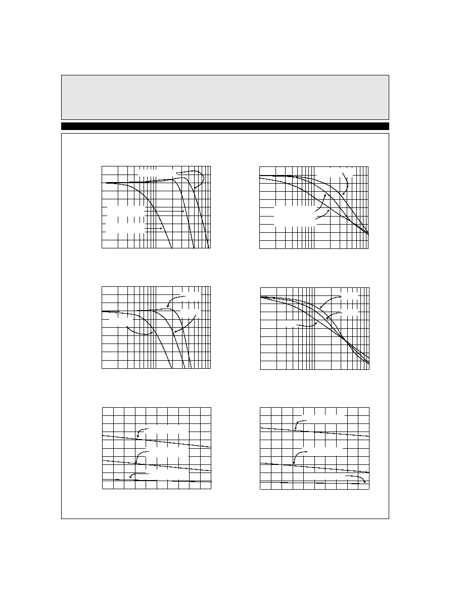
Typical Performance Curves
Inverting Frequency Response (Gain)
V
CM
= 1.5V, R
F
= 1K
,
R
L
= 150
1M
10M
100M
-6
-4
-2
0
+2
M
A
G
N
I
T
UDE
(
NORM
A
I
L
Z
E
D)
(
d
B)
FREQUENCY (Hz)
1
A
V
= -1
A
V
= -2
A
V
= -5.6
Inverting Frequency Response (Phase)
V
CM
= 1.5V, R
F
= 1K
,
R
L
= 150
1M
10M
100M
0
45
90
135
180
P
HAS
E
(
∞
)
FREQUENCY (Hz)
2
A
V
= -1
A
V
= -2
A
V
= -5.6
Non-Inverting Frequency Response (Gain)
V
CM
= 1.5V, R
L
= 150
1M
10M
100M
-8
-6
-4
-2
0
M
AGNI
T
UDE
(
NORM
A
L
I
Z
E
D)
(
d
B)
FREQUENCY (Hz)
19
A
V
= +1, R
F
= 0
+2
A
V
= +2, R
F
= 1K
A
V
= +5.6, R
F
= 1K
Non-Inverting Frequency Response (Phase)
V
CM
= 1.5V, R
L
= 150
1M
10M
100M
-180
-135
-90
-45
0
FREQUENCY(Hz)
15
P
HAS
E
(
∞
)
A
V
= +2, R
F
= 1K
A
V
= +1, R
F
= 0
A
V
= +5.6, R
F
= 1K
3dB Bandwidth vs. Die Temperature for Various Gains
RL = 10K
3dB
BA
NDWI
D
T
H
(
M
Hz)
DIE TEMPERATURE (∞C)
51
0
30
60
90
120
-55
-15
25
65
145
105
145
150
A
V
= +1, R
F
= 0
A
V
= +2, R
F
= 1K
A
V
= +5.6, R
F
= 1K
3dB Bandwidth vs. Die Temperature for Various Gains
RL = 150
3dB BANDW
I
D
T
H
(
M
H
z
)
DIE TEMPERATURE (∞C)
52
0
20
40
60
80
-55
-15
25
65
145
105
145
100
A
V
= +1, R
F
= 0
A
V
= +2, R
F
= 1K
A
V
= +5.6, R
F
= 1K

5
EL5144C, EL5146C, EL5244C, EL5246C,
EL5444C
100 MHz Single Supply Rail to Rail Amplifier
EL
5144C, EL5146
C
,
E
L
5244C, EL
5246C, EL5444C
Group Delay vs. Frequency
1M
10M
100M
GROUP
DE
L
AY (
n
s
ec)
FREQUENCY (Hz)
23
0
2
4
6
8
10
A
V
= +2
R
F
= 1K
A
V
= +1
R
F
= 0
Frequency Response for Various R
L
V
CM
= 1.5V, R
F
= 0
,
A
V
= +1
1M
10M
100M
-4
-2
0
+2
+4
M
AGNI
T
UDE
(
NOR
M
A
L
I
Z
E
D)
(
d
B)
FREQUENCY (Hz)
16
R
L
= 10K
R
L
= 520
R
L
= 150
R
L
= 520
Frequency Response for Various C
L
V
CM
= 1.5V, R
L
= 150
,
A
V
= +1
1M
10M
100M
-8
-4
0
+4
+8
M
A
G
N
I
T
UDE
(
NORM
A
L
I
Z
E
D)
(
d
B)
FREQUENCY (Hz)
17
C
L
= 47pF
C
L
= 22pF
C
L
= 0pF
C
L
= 100pF
Frequency Response for Various R
F
and R
G
V
CM
= 1.5V,R
L
= 150
,
A
V
= +2
1M
10M
100M
-4
-2
0
+2
M
AGNI
T
UDE
(
NORM
A
L
I
Z
E
D)
(
d
B)
FREQUENCY (Hz)
18
R
F
= R
G
= 1K
R
F
= R
G
= 560
-6
R
F
= R
G
= 2K
Open Loop Gain and Phase vs. Frequency
1K
100K
10M
G
A
IN
(d
B
)
FREQUENCY (Hz)
29
0
20
40
60
80
R
L
= 1K
Gain
R
L
= 150
Phase
180
135
90
45
0
P
HAS
E
(
∞
)
Open Loop Voltage Gain vs. Die Temperature
OP
E
N
L
OOP
G
A
I
N
(
d
B
)
DIE TEMPERATURE (∞C)
43
30
40
50
60
70
-55
-15
25
65
145
105
145
80
No Load
R
L
=150