Note: All information contained in this data sheet has been carefully checked and is believed to be accurate as of the date of publication; however, this data sheet cannot be a "controlled document". Current revisions, if any, to these
specifications are maintained at the factory and are available upon your request. We recommend checking the revision level before finalization of your design documentation.
© 2001 Elantec Semiconductor, Inc.
EL
5825C -
Preliminary
General Description
The EL5825C is designed to produce the reference voltages required
in TFT-LCD applications. Each output is programmed to the required
voltage with 10 bits of resolution. Reference pins determine the high
and low voltages of the output range, which are capable of swinging to
either supply rail. Programming of each output is performed using the
serial interface. A serial out pin enables daisy chaining of multiple
devices.
A number of the EL5825C can be stacked for applications requiring
more than 8 outputs. The reference inputs can be tied to the rails,
enabling each part to output the full voltage range, or alternatively,
they can be connected to external resistors to split the output range and
enable finer resolutions of the outputs.
The EL5825C has 8 outputs and is available in both the 24-pin TSSOP
and the 24-pin LPP packages. It is specified for operation over the full
-40∞C to +85∞C temperature range.
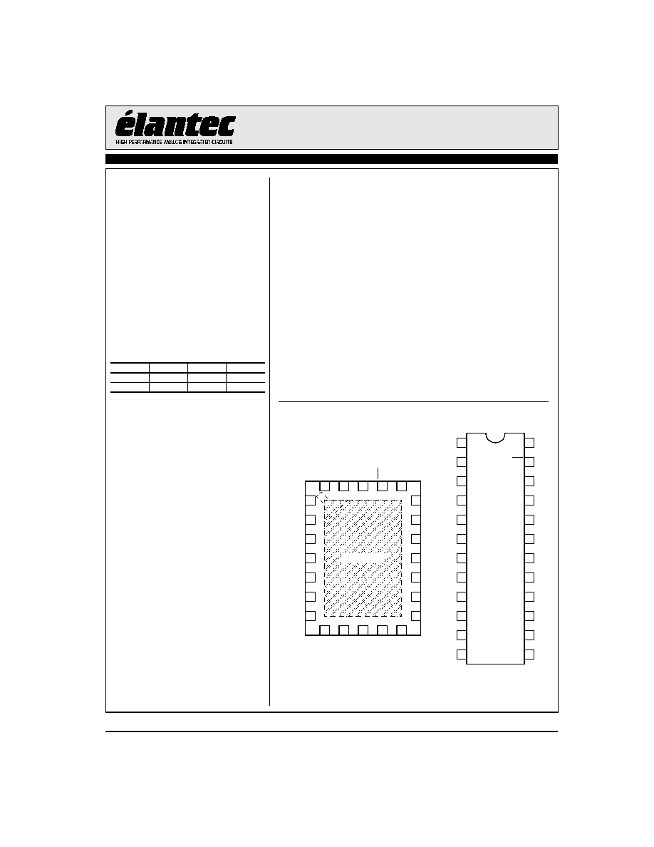
Connection Diagram
19
18
17
16
15
14
13
24
23
22
21
20
8
9
10
11
12
1
2
3
4
5
6
7
24-Pin LPP Top View
Thermal Pad
OSC
VSD
VS
REFH
REFL
GND
OUTB
OUTC
OUTD
GND
OUTE
OUTF
OUTG
SD
O
SC
L
K
SD
I
EN
A
OU
TA
BC
HO
L
D
OU
TH
24-Pin TSSOP
1
2
3
4
16
15
14
13
5
6
7
12
11
9
8
10
20
19
18
17
24
23
22
21
SCLK
SD1
SDO
ENA
OSC
OUT A
VSD
OUT B
NC
OUT C
VS
OUT D
REFH
GND
REFL
OUT E
GND
OUT F
NC
OUT G
BG HOLD
OUT H
NC
NC
Features
∑
8-channel reference outputs
∑
Accuracy of ±0.1%
∑
Supply voltage of 5V to 16V
∑
Digital supply 3.3V to 5V
∑
Low supply current of 10mA
∑
Rail-to-rail capability
Applications
∑
TFT-LCD drive circuits
∑
Reference voltage generators
Ordering Information
Part No
Package
Tape & Reel
Outline #
EL5825CU
24-Pin LPP
-
MDP0046
EL5825CR
24-Pin TSSOP
-
MDP0044
EL5825C - Preliminary
8-Channel TFT-LCD Reference Voltage Generator
O
c
tob
e
r 4, 2001
2
EL5825C - Preliminary
8-Channel TFT-LCD Reference Voltage Generator
EL
5825C
-
Pre
l
iminary
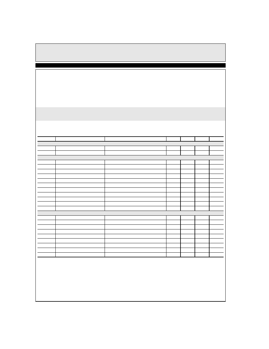
Absolute Maximum Ratings
(T
A
= 25∞C)
Values beyond absolute maximum ratings can cause the device to be pre-
maturely damaged. Absolute maximum ratings are stress ratings only and
functional device operation is not implied.
Supply Voltage between V
S
and GND
+18V
Supply Voltage between V
SD
and GND
V
S
and +7V (min)
Maximum Continuous Output Current
30mA
Maximum Die Temperature
+125∞C
Storage Temperature
-65∞C to +150∞C
Operating Temperature
-40∞C to +85∞C
Lead Temperature
260∞C
Power Dissipation
See Curves
ESD Voltage
2kV
Important Note:
All parameters having Min/Max specifications are guaranteed. Typ values are for information purposes only. Unless otherwise noted, all tests are at the
specified temperature and are pulsed tests, therefore: T
J
= T
C
= T
A
.
Electrical Characteristics
V
S
= 15V, V
SD
= 5V, V
REFH
= 13V, V
REFL
= 2V, R
L
= 1.5k
and C
L
= 200pF to 0V, T
A
= 25∞C unless otherwise specified.
Parameter
Description
Condition
Min
Typ
Max
Unit
Supply
I
S
Supply Current
No load
10
TBD
mA
I
SD
Digital Supply Current
1
mA
Analog
V
OL
Output Swing Low
R
L
= 1.5k
to 7.5V, after 1mS
100
200
mV
V
OH
Output Swing High
R
L
= 1.5k
to 7.5V, after 1mS
14.75
14.9
V
I
SC
Short Circuit Current
R
L
= 10
100
mA
PSRR
Power Supply Rejection Ratio
V
S
+ is moved from 14V to 16V
TBD
TBD
dB
V
OS
Offset Voltage
V
OUT
= V
S
/ 2
2
5
mV
t
D
Program to Out Delay
TBD
mS
V
AC
Accuracy
TBD
12
mV
V
DROOP
Droop Voltage
TBD
15
mV/mS
R
INH
Input Resistance @ VREFH
V
REFH
= 15V
32
k
R
INL
Input Resistance @ VREFL
V
REFL
= 0V
32
kW
REG
Load Regulation
I
OUT
= 5mA step
2
mV
Digital
V
IH
Logic 1 Input Voltage
V
SD
-20%
V
V
IL
Logic 0 Input Voltage
20%*V
SD
V
F
CLK
Clock Frequency
5
MHz
t
S
Setup Time
10
ns
t
H
Hold Time
10
ns
t
LC
Load to Clock Time
10
ns
t
CE
Clock to Load Line
10
ns
t
DCO
Clock to Out Delay Time
ns
R
SDIN
S
DIN
Input Resistance
1
G

3
EL5825C - Preliminary
8-Channel TFT-LCD Reference Voltage Generator
EL
5825C
-
Pre
l
iminary
General Disclaimer
Specifications contained in this data sheet are in effect as of the publication date shown. Elantec, Inc. reserves the right to make changes in the cir-
cuitry or specifications contained herein at any time without notice. Elantec, Inc. assumes no responsibility for the use of any circuits described
herein and makes no representations that they are free from patent infringement.
WARNING - Life Support Policy
Elantec, Inc. products are not authorized for and should not be used
within Life Support Systems without the specific written consent of
Elantec, Inc. Life Support systems are equipment intended to sup-
port or sustain life and whose failure to perform when properly used
in accordance with instructions provided can be reasonably
expected to result in significant personal injury or death. Users con-
templating application of Elantec, Inc. Products in Life Support
Systems are requested to contact Elantec, Inc. factory headquarters
to establish suitable terms & conditions for these applications. Elan-
tec, Inc.'s warranty is limited to replacement of defective
components and does not cover injury to persons or property or
other consequential damages.
Elantec Semiconductor, Inc.
675 Trade Zone Blvd.
Milpitas, CA 95035
Telephone: (408) 945-1323
(800) ELANTEC
Fax:
(408) 945-9305
European Office: 44-118-977-6020
October
4, 200
1
Printed in U.S.A.
Japan Technical Center: 81-45-682-5820