
© 2000 Elantec Semiconductor, Inc.
EL
7156C
General Description
The EL7156C high-performance pin driver with tri-state is suited to
many ATE and level-shifting applications. The 3.5A peak drive capa-
bility makes this part an excellent choice when driving high
capacitance loads.
The output pin OUT is connected to input pins VH or VL respectively,
depending on the status of the IN pin. When the OE pin is active low,
the output is placed in the tri-state mode. The isolation of the output
FETs from the power supplies enables VH and VL to be set indepen-
dently, enabling level-shifting to be implemented. Related to the
EL7155C, the EL7156C adds a lower supply pin V
S
- and makes VL
an isolated and independent input. This feature adds applications flex-
ibility and improves switching response due to the increased
enhancement of the output FETs.
This pin driver has improved performance over existing pin drivers. It
is specifically designed to operate at voltages down to 0V across the
switch elements while maintaining good speed and on-resistance
characteristics.
Available in the 8-Pin SOIC and 8-Pin PDIP packages, the EL7156C is
specified for operation over the -40∞C to +85∞C temperature range.
Pin Configuration
1
2
3
4
8
7
6
5
8-Pin PDIP/SOIC
VH
L
o
g
i
c
OUT
VL
V
S
-
V
S
+
OE
IN
GND
Features
∑ Clocking Speeds up to 40MHz
∑ 15ns tr/tf at 2000pF C
LOAD
∑ 0.5ns Rise and Fall Times
Mismatch
∑ 0.5ns T
ON
-T
OFF
Prop Delay
Mismatch
∑ 3.5pF Typical Input Capacitance
∑ 3.5A Peak Drive
∑ Low on Resistance of 3.5
∑ High Capacitive Drive Capability
∑ Operates from 4.5V to 18V
Applications
∑ ATE/Burn-in Testers
∑ Level Shifting
∑ IGBT Drivers
∑ CCD Drivers
Ordering Information
Part No.
Package
Tape & Reel
Outline #
EL7156CN
8-Pin DIP
-
MDP0031
EL7156CS
8-Pin SOIC
-
MDP0027
EL7156CS-T7
8-Pin SOIC
7"
MDP0027
EL7156CS-T13
8-Pin SOIC
13"
MDP0027
EL7156C
High Performance Pin Driver
Septe
m
ber 5, 2000

2
EL7156C
High Performance Pin Driver
E
L
7156C
Absolute Maximum Ratings
(T
A
= 25∞C)
Absolute maximum ratings are those values beyond which the device
could be permanently damaged. Absolute maximum ratings are stress
ratings only and functional device operation is not implied.
Supply Voltage (V
S
+ to V
S
-)
+18V
Input Voltage
V
S
- -0.3V, V
S
+0.3V
Continuous Output Current
200mA
Storage Temperature Range
-65∞C to +150∞C
Ambient operating Temperature
-40∞C to +85∞C
Operating Junction Temperature
125∞C
Power Dissipation
see curves
Maximum ESD
2kV
Important Note:
All parameters having Min/Max specifications are guaranteed. Typ values are for information purposes only. Unless otherwise noted, all tests are at the
specified temperature and are pulsed tests, therefore: T
J
= T
C
= T
A
.
Electrical Characteristics
V
S
+ = +15V, VH = +15V, VL = 0V, V
S
-=0V, T
A
= 25∞C, unless otherwise specified
Parameter
Description
Condition
Min
Typ
Max
Units
Input
V
IH
Logic `1' Input Voltage
2.4
V
I
IH
Logic `1' Input Current
V
IH
= V
S
+
0.1
10
µ A
V
IL
Logic `0' Input Voltage
0.8
V
I
IL
Logic `0' Input Current
V
IL
= 0V
0.1
10
µ A
C
IN
Input Capacitance
3.5
pF
R
IN
Input Resistance
50
M
Output
R
OVH
ON Resistance VH to OUT
I
OUT
= -200 mA
2.7
4.5
R
OVL
ON Resistance VL to OUT
I
OUT
= +200 mA
3.5
5.5
I
OUT
Output Leakage Current
OE = 0V, OUT = VH/VL
0.1
10
µ A
I
PK
Peak Output Current
(linear resistive operation)
Source
3.5
A
Sink
3.5
A
I
DC
Continuous Output Current
Source/Sink
200
mA
Power Supply
I
S
Power Supply Current
Inputs = V
S
+
1.3
3
mA
I
VH
Off Leakage at VH
and VL
VH, VL = 0V
4
10
µ A
Switching Characteristics
t
R
Rise Time
C
L
=2000 pF
14.5
ns
t
F
Fall Time
C
L
= 2000 pF
15
ns
t
RFdelta
t
R
, t
F
Mismatch
C
L
= 2000 pF
0.5
ns
t
D-1
Turn-Off Delay Time
C
L
= 2000 pF
9.5
ns
t
D-2
Turn-On Delay Time
C
L
= 2000 pF
10
ns
t
Ddelta
t
D-1
-t
D-2
Mismatch
C
L
= 2000 pF
0.5
ns
t
D-3
Tri-State Delay Enable
10
ns
t
D-4
Tri-State Delay Disable
10
ns

3
EL7156C
High Performance Pin Driver
EL
7156C
Electrical Characteristics
V
S
+ = +5V, VH = +5V, VL = -5V, V
S
- = -5V, T
A
= 25∞C, unless otherwise specified
Parameter
Description
Condition
Min
Typ
Max
Units
Input
V
IH
Logic `1' Input Voltage
2.0
V
I
IH
Logic `1' Input Current
V
IH
= V
S
+
0.1
10
µ A
V
IL
Logic `0' Input Voltage
0.8
V
I
IL
Logic `0' Input Current
V
IL
= 0V
0.1
10
µ A
C
IN
Input Capacitance
3.5
pF
R
IN
Input Resistance
50
M
Output
R
OVH
ON Resistance VH to OUT
I
OUT
= -200 mA
3.4
5
R
OVL
ON Resistance VL to OUT
I
OUT
= +200 mA
4
6
I
OUT
Output Leakage Current
OE = 0V, OUT = VH/VL
0.1
10
µ A
I
PK
Peak Output Current
(linear resistive operation)
Source
3.5
A
Sink
3.5
A
I
DC
Continuous Output Current
Source/Sink
200
mA
Power Supply
I
S
Power Supply Current
Inputs = V
S
+
1
2.5
mA
V
H
Off Leakage at VH and VL
VH, VL = 0V
4
10
µ A
Switching Characteristics
t
R
Rise Time
C
L
= 2000 pF
17
ns
t
F
Fall Time
C
L
= 2000 pF
17
ns
t
RFdelta
t
R
, t
F
Mismatch
C
L
= 2000 pF
0
ns
t
D-1
Turn-Off Delay Time
C
L
= 2000 pF
11.5
ns
t
D-2
Turn-On Delay Time
C
L
= 2000 pF
12
ns
t
Ddelta
t
D-1
-t
D-2
Mismatch
C
L
= 2000 pF
0.5
ns
t
D-3
Tri-State Delay Enable
10
ns
t
D-4
Tri-State Delay Disable
10
ns

4
EL7156C
High Performance Pin Driver
E
L
7156C
Typical Performance Curves
Input Threshold vs Supply Voltage
T=25∞C
1.2
I
nput
v
o
l
t
age (V
)
Supply Voltage (V)
1.0
1.8
1.6
1.4
15
5
10
High Threshold
Hysteresis
Quiescent Supply Current vs Supply Voltage
T=25∞C
15
S
uppl
y
C
u
rr
ent
(
m
A
)
Supply Voltage (V)
0
2.0
5
1.6
1.2
0.8
0.4
10
All Inputs = GND
All Inputs = V
S
+
Rise/Fall Time vs Supply Voltage
C
L
=2000pF, T=25∞C
15
20
Ri
se
/F
a
l
l
T
i
m
e
(
n
s)
Supply Voltage (V)
10
30
5
Rise/Fall Time vs Temperature
C
L
=2000pF, V
S
+=15V
150
14
R
i
se
/
F
a
l
l
T
i
m
e
(n
s)
Temperature (∞C)
10
100
20
-50
10
25
15
50
16
18
12
0
Low Threshold
t
F
t
R
t
R
t
I
t
R
t
F
"On" Resistance vs Supply Voltage
I
OUT
=200mA, T=25∞C, V
S
+=VH, V
S
-=VL=0V
"
On
"
Res
i
s
t
anc
e (
)
Supply Voltage (V)
7.5
15
12.5
5
10
1
0
6
5
2
4
3
V
OUT
-VL
V
OUT
-VH
Max Power/Derating Curves
M
a
x P
o
we
r (W)
Temperature (∞C)
25
100
75
0
50
200mW
1W
600mW
400mW
800mW
125
150
0
Max T
J
=125∞C
JA
=160∞C/W
8-Lead SO
8-Lead PDIP
JA
=100∞C/W
5
EL7156C
High Performance Pin Driver
EL
7156C
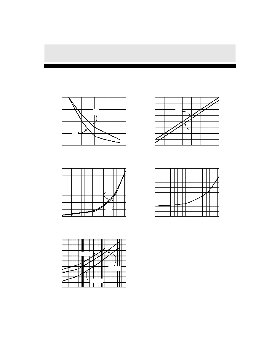
Typical Performance Curves
Propagation Delay vs Supply Voltage
C
L
=2000pF, T=25∞C
15
13
Del
a
y
T
i
m
e
(n
s)
Supply Voltage (V)
9
17
5
Propagation Delay vs Temperature
C
L
=2000pF, V
S
+=15V
Del
a
y
T
i
m
e
(n
s)
Temperature (∞C)
6
14
15
11
10
0
125
-50
50
12
8
-25
25
75
100
1M
10M
10k
100k
0.1
1.0
10
100
Supply Current vs Frequency
C
L
=1000pF, T=25∞C
S
upp
l
y
Cur
r
ent
(m
A
)
Frequency (Hz)
10
Rise/Fall Time vs Load Capacitance
V
S
+=+15V, T=25∞C
10000
30
R
i
se
/
F
a
l
l
T
i
m
e
(
n
s)
Load Capacitance (pF)
0
70
100
1000
60
50
40
20
10
t
D-2
t
D-1
t
D-2
t
D-1
t
F
t
R
V
S
+=15V
V
S
+=10V
V
S
+=5V
100
1000
10000
0
1
4
5
3
2
Supply Current vs Load Capacitance
V
S
+=VH=15V, V
S
-=VL=0V, T=25∞C, f=20kHz
S
uppl
y
C
u
rr
ent
(
m
A
)
Load Capacitance (pF)