EL7202CEL7212CEL7222C
January
1996
Rev
B
EL7202C 7212C 7222C
High Speed Dual Channel Power MOSFET Drivers
Note All information contained in this data sheet has been carefully checked and is believed to be accurate as of the date of publication however this data sheet cannot be a ``controlled document'' Current revisions if any to these
specifications are maintained at the factory and are available upon your request We recommend checking the revision level before finalization of your design documentation
1994 Elantec Inc
Features
Industry standard driver
replacement
Improved response times
Matched rise and fall times
Reduced clock skew
Low output impedance
Low input capacitance
High noise immunity
Improved clocking rate
Low supply current
Wide operating voltage range
Applications
Clock line drivers
CCD Drivers
Ultra-sound transducer drivers
Power MOSFET drivers
Switch mode power supplies
Class D switching amplifiers
Ultrasonic and RF generators
Pulsed circuits
Ordering Information
Part No
Temp Range
Pkg
Outline
EL7202CN b40 C to a85 C 8-Pin P-DIP MDP0031
EL7202CS b40 C to a85 C 8-Pin SO
MDP0027
EL7212CN b40 C to a85 C 8-Pin P-DIP MDP0031
EL7212CS b40 C to a85 C 8-Pin SO
MDP0027
EL7222CN b40 C to a85 C 8-Pin P-DIP MDP0031
EL7222CS b40 C to a85 C 8-Pin SO
MDP0027
General Description
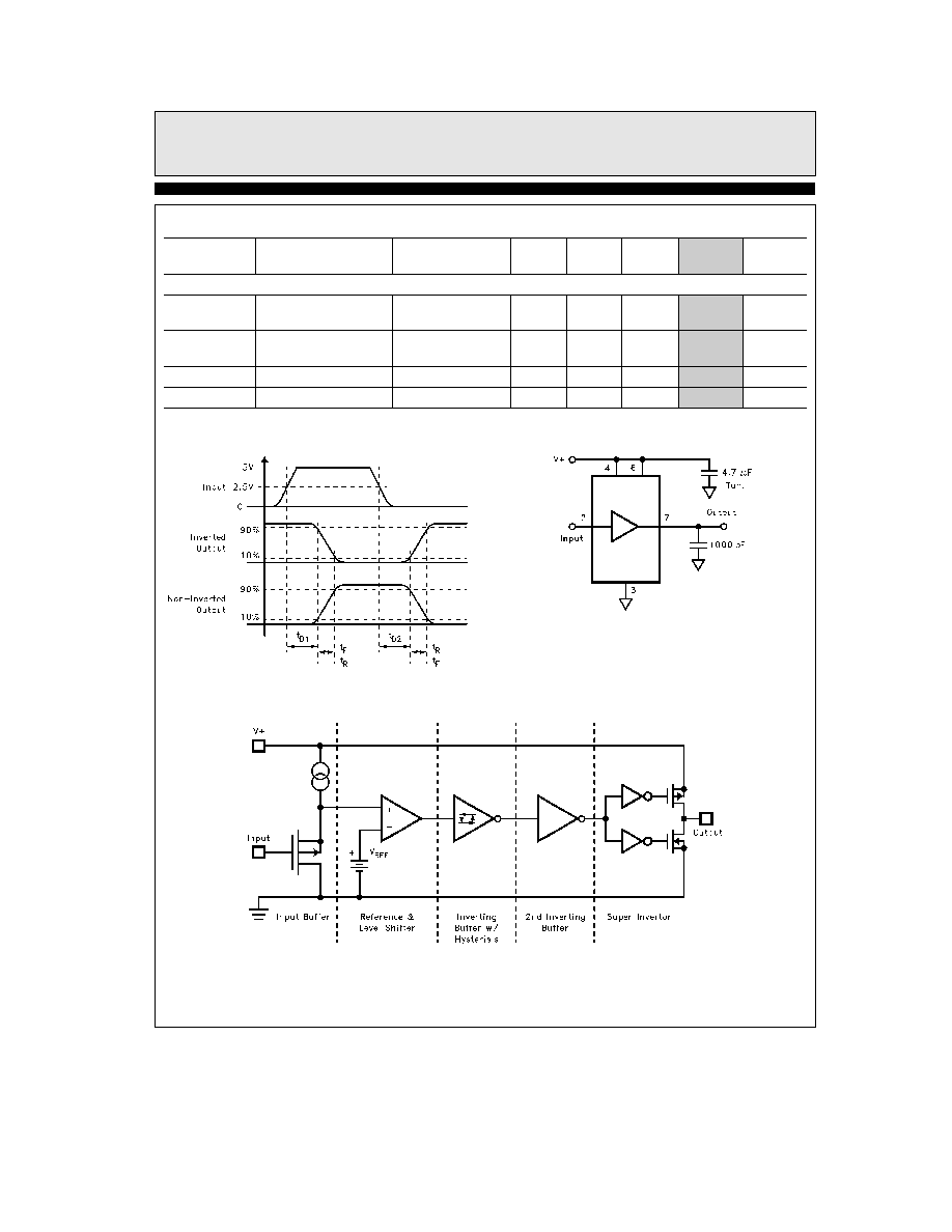
The EL7202C EL7212C EL7222C ICs are matched dual-driv-
ers ICs that improve the operation of the industry standard
DS0026 clock drivers The Elantec Versions are very high speed
drivers capable of delivering peak currents of 2 0 amps into
highly capacitive loads The high speed performance is achieved
by means of a proprietary ``Turbo-Driver'' circuit that speeds
up input stages by tapping the wider voltage swing at the out-
put Improved speed and drive capability are enhanced by
matched rise and fall delay times These matched delays main-
tain the integrity of input-to-output pulse-widths to reduce tim-
ing errors and clock skew problems This improved performance
is accompanied by a 10 fold reduction in supply currents over
bipolar drivers yet without the delay time problems commonly
associated with CMOS devices Dynamic switching losses are
minimized with non-overlapped drive techniques
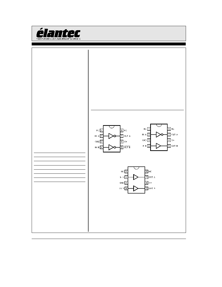
Connection Diagrams
EL7222C
EL7212C
7202 � 2
7202 � 1
Complementary Drivers
Inverting Drivers
EL7202C
7202 � 3
Non-Inverting Drivers
Manufactured under U S Patent Nos 5 334 883
5 341 047
EL7202C EL7212C EL7222C
High Speed Dual Channel Power MOSFET Drivers
Absolute Maximum Ratings
Supply (V
a
to Gnd)
16 5V
Input Pins
b
0 3V to
a
0 3V above V
a
Combined Peak Output Current
4A
Storage Temperature Range
b
65 C to
a
150 C
Ambient Operating Temperature
b
40 C to
a
85 C
Operating Junction Temperature
125 C
Power Dissipation
SOIC
570 mW
PDIP
1050 mW
Important Note
All parameters having Min Max specifications are guaranteed The Test Level column indicates the specific device testing actually
performed during production and Quality inspection Elantec performs most electrical tests using modern high-speed automatic test
equipment specifically the LTX77 Series system Unless otherwise noted all tests are pulsed tests therefore T
J
e
T
C
e
T
A
Test Level
Test Procedure
I
100% production tested and QA sample tested per QA test plan QCX0002
II
100% production tested at T
A
e
25 C and QA sample tested at T
A
e
25 C
T
MAX
and T
MIN
per QA test plan QCX0002
III
QA sample tested per QA test plan QCX0002
IV
Parameter is guaranteed (but not tested) by Design and Characterization Data
V
Parameter is typical value at T
A
e
25 C for information purposes only
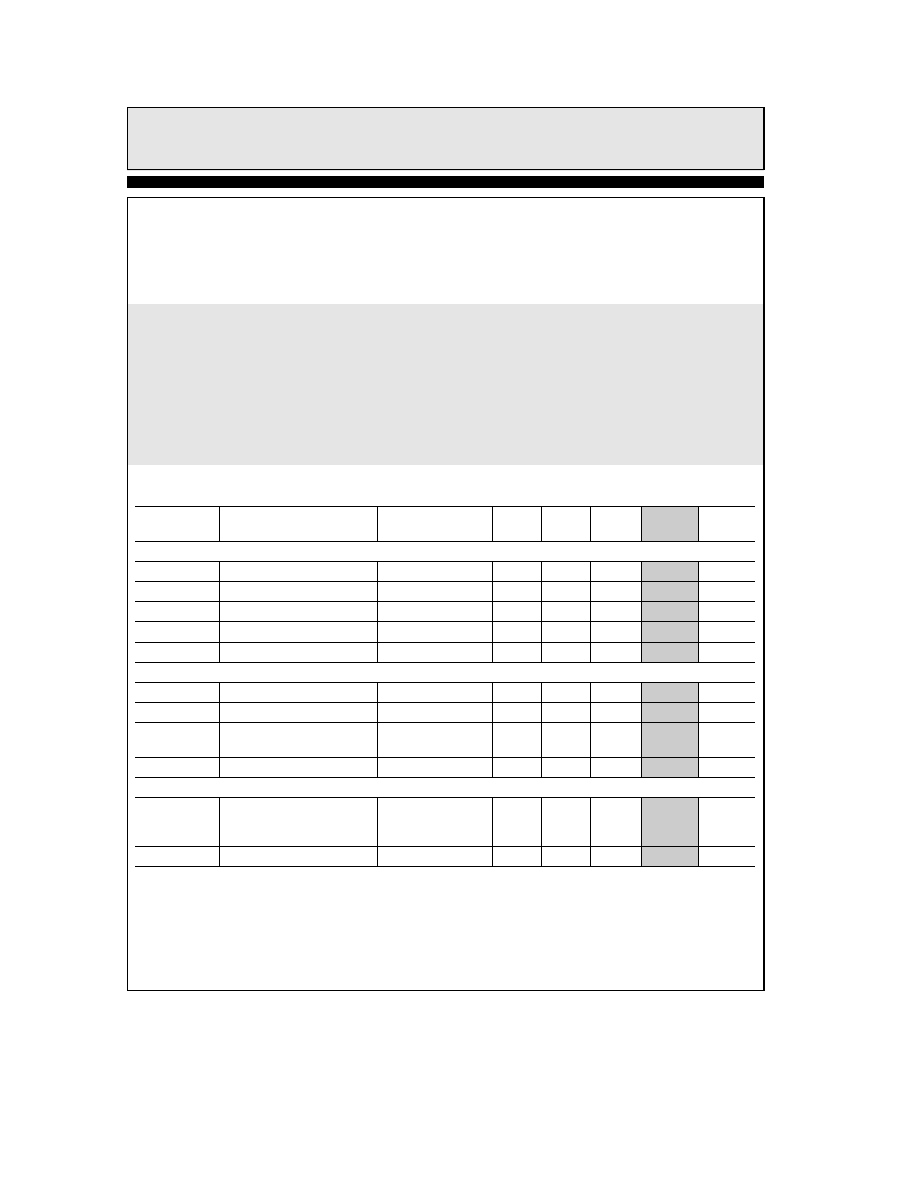
DC Electrical Characteristics
T
A
e
25 C V
e
15V unless otherwise specified
Parameter
Description
Test
Min
Typ
Max
Test
Units
Conditions
Level
Input
V
IH
Logic ``1'' Input Voltage
2 4
I
V
I
IH
Logic ``1'' Input Current
V
a
0 1
10
I
mA
V
IL
Logic ``0'' Input Voltage
0 8
I
V
I
IL
Logic ``0'' Input Current
0V
0 1
10
I
mA
V
HVS
Input Hysteresis
0 3
V
V
Output
R
OH
Pull-Up Resistance
I
OUT
e b
100 mA
3
6
I
X
R
OL
Pull-Down Resistance
I
OUT
e a
100 mA
4
6
I
X
I
PK
Peak Output Current
Source
2
IV
A
Sink
2
I
DC
Continuous Output Current
Source Sink
100
I
mA
Power Supply
I
S
Power Supply Current
Inputs High 7202
4 5
7 5
I
Inputs High 7212
1
2 5
I
mA
Inputs High 7222
2 5
5 0
I
V
S
Operating Voltage
4 5
15
I
V
2
TD
is
33in
EL7202C EL7212C EL7222C
High Speed Dual Channel Power MOSFET Drivers
AC Electrical Characteristics
T
A
e
25 C V
e
15V unless otherwise specified
Parameter
Description
Test
Min
Typ
Max
Test
Units
Conditions
Level
Switching Characteristics
t
R
Rise Time
C
L
e
500 pF
7 5
IV
ns
C
L
e
1000 pF
10
20
t
F
Fall Time
C
L
e
500 pF
10
IV
ns
C
L
e
1000 pF
13
20
t
D1
Turn-On Delay Time
See Timing Table
18
25
IV
ns
t
D2
Turn-Off Delay Time
See Timing Table
20
25
IV
ns
Timing Table
7202 � 4
Standard Test Configuration
7202 � 19
Simplified Schematic
7202 � 5
3
TD
is
15in
EL7202C EL7212C EL7222C
High Speed Dual Channel Power MOSFET Drivers
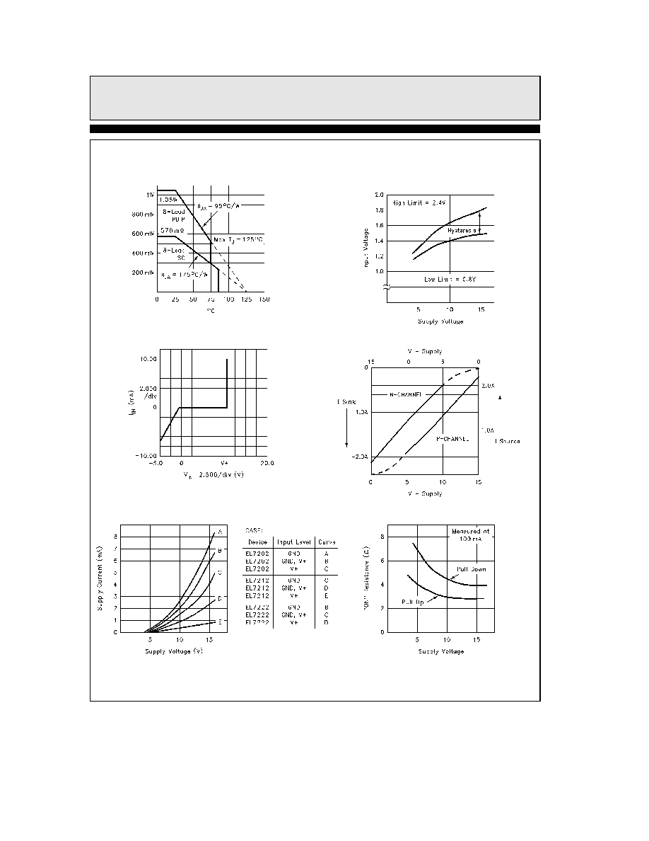
Typical Performance Curve
Max Power Derating Curves
7202 � 6
Switch Threshold vs
Supply Voltage
7202 � 7
Input Current vs Voltage
7202 � 8
Peak Drive vs Supply Voltage
7202 � 9
Quiescent Supply Current
7202 � 10
``ON'' Resistance vs Supply Voltage
7202 � 11
4
EL7202C EL7212C EL7222C
High Speed Dual Channel Power MOSFET Drivers
Typical Performance Curve
Contd
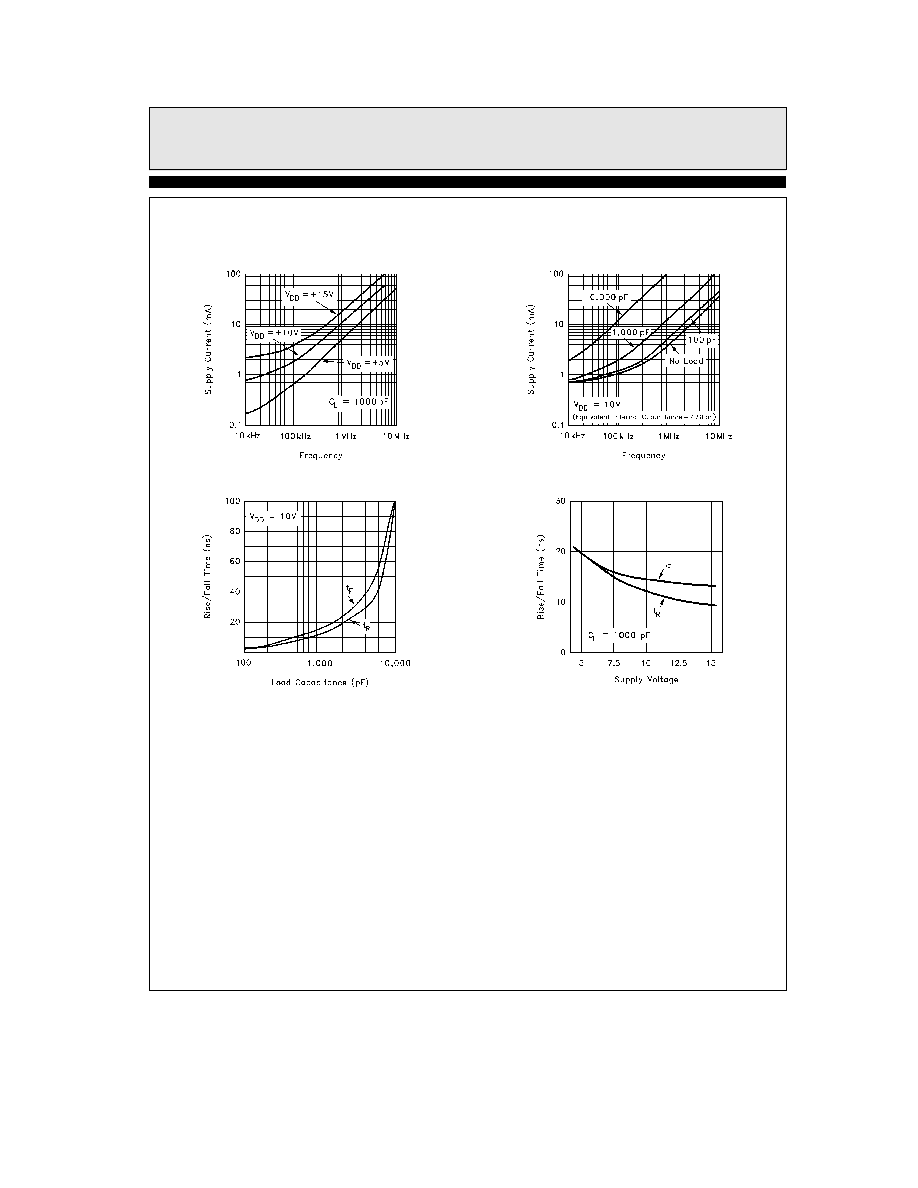
Average Supply Current vs
Voltage and Frequency
7202 � 12
Average Supply Current
vs Capacitive Load
7202 � 13
Rise Fall Time vs Load
7202 � 14
Rise Fall Time vs Supply Voltage
7202 � 15
5
EL7202C EL7212C EL7222C
High Speed Dual Channel Power MOSFET Drivers
Typical Performance Curve
Contd
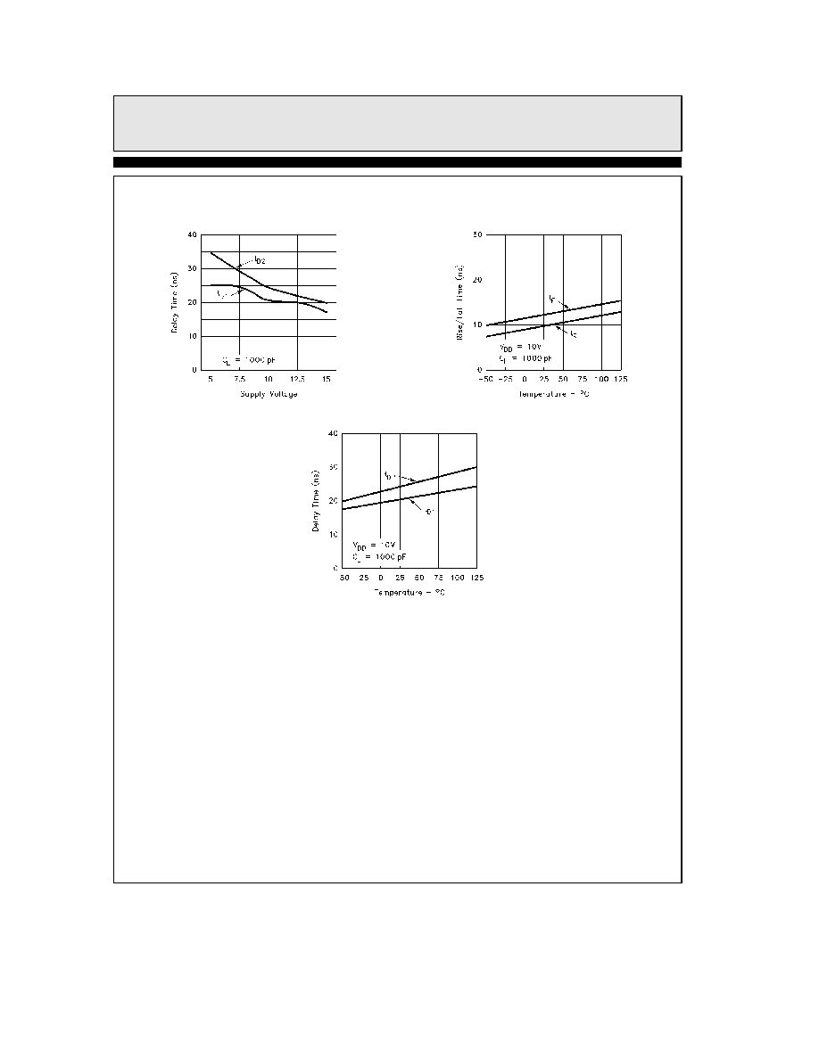
Propagation Delay vs Supply Voltage
7202 � 16
Rise Fall Time vs Temperature
7202 � 17
Delay vs Temperature
7202 � 18
6
EL7202C EL7212C EL7222C
High Speed Dual Channel Power MOSFET Drivers
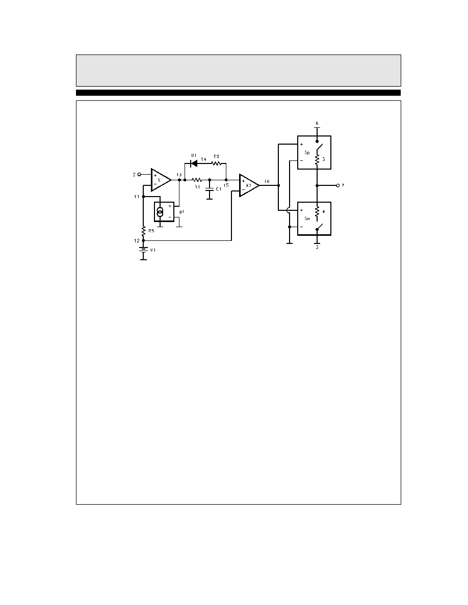
EL7212 Macro Model
7202 � 20
EL7212 model
input
l
gnd
l
l
Vsupply
l
l
l
Vout
subckt M7212 2
3
6
7
V1 12 3 1 6
R1 13 15 1k
R2 14 15 5k
R5 11 12 100
C1 15 3 43 3 pF
D1 14 13 dmod
X1 13 11 2 3 comp1
X2 16 12 15 3 comp1
sp 6 7 16 3 spmod
sn 7 3 16 3 snmod
g1 11 0 13 0 938
m
model dmod d
model spmod vswitch ron
43 roff42meg von41 voff41 5
model snmod vswitch ron
44 roff42meg von43 voff42
ends M7212
subckt comp1 out inp inm vss
e1 out vss table
(v(inp)
1v(inm)) 5000 4 (0 0) (3 2 3 2)
Rout out vss 10meg
Rinp inp vss 10meg
Rinm inm vss 10meg
ends comp1
7
TD
is
36in

EL7202CEL7212CEL7222C
January
1996
Rev
B
EL7202C EL7212C EL7222C
High Speed Dual Channel Power MOSFET Drivers
General Disclaimer
Specifications contained in this data sheet are in effect as of the publication date shown Elantec Inc reserves the right to make changes
in the circuitry or specifications contained herein at any time without notice Elantec Inc assumes no responsibility for the use of any
circuits described herein and makes no representations that they are free from patent infringement
Elantec Inc
1996 Tarob Court
Milpitas CA 95035
Telephone (408) 945-1323
(800) 333-6314
Fax (408) 945-9305
European Office 44-71-482-4596
WARNING
Life Support Policy
Elantec Inc products are not authorized for and should not be
used within Life Support Systems without the specific written
consent of Elantec Inc Life Support systems are equipment in-
tended to support or sustain life and whose failure to perform
when properly used in accordance with instructions provided can
be reasonably expected to result in significant personal injury or
death Users contemplating application of Elantec Inc products
in Life Support Systems are requested to contact Elantec Inc
factory headquarters to establish suitable terms
conditions for
these applications Elantec Inc 's warranty is limited to replace-
ment of defective components and does not cover injury to per-
sons or property or other consequential damages
Printed in U S A
8