Note: All information contained in this data sheet has been carefully checked and is believed to be accurate as of the date of publication; however, this data sheet cannot be a "controlled document". Current revisions, if any, to these
specifications are maintained at the factory and are available upon your request. We recommend checking the revision level before finalization of your design documentation.
© 2001 Elantec Semiconductor, Inc.
E
L
7
5
6
4
C
General Description
The EL7564C is an integrated, full-featured synchronous step-down
regulator with output voltage adjustable from 1.0V to 3.8V. It is capa-
ble of delivering 4A continuous current at up to 95% efficiency. The
EL7564C operates at a constant frequency pulse width modulation
(PWM) mode, making external synchronization possible. Patented on-
chip resistorless current sensing enables current mode control, which
provides cycle-by-cycle current limiting, over-current protection, and
excellent step load response. The EL7564C features power tracking,
which makes the start-up sequencing of multiple converters possible.
A junction temperature indicator conveniently monitors the silicon die
temperature, saving the designer time on the tedious thermal charac-
terization. The minimal external components and full functionality
make this EL7564C ideal for desktop and portable applications.
The EL7564C is specified for operation over the -40∞C to +85∞C tem-
perature range.
Typical Application Diagrams
Manufactured Under U.S. Patent No. 5,7323,974
1
2
3
4
16
15
14
13
5
6
7
12
11
9
8
10
EL7564CM
(20-Pin SO)
20
19
18
17
0.1µF
390pF
0.22µF
22
2.2nF
330µF
V
IN
5V
V
OUT
3.3V,
4A
2.37k
1k
330µF
0.22µF
4.7µH
VREF
SGND
COSC
VDD
VTJ
PGND
PGND
VIN
STP
STN
EN
FB
PG
VDRV
VHI
LX
LX
PGND
PGND
PGND
2.2nF
C5
C4
R4
C3
C2
C1
C6
D1
L1
C7
R2
C10
R1
Typical Application Diagrams continued on page 3
Features
∑ Integrated synchronous MOSFETs
and current mode controller
∑ 4A continuous output current
∑ Up to 95% efficiency
∑ 4.5V to 5.5V input voltage
∑ Adjustable output from 1V to 3.8V
∑ Cycle-by-cycle current limit
∑ Precision reference
∑ ±0.5% load and line regulation
∑ Adjustable switching frequency to
1MHz
∑ Oscillator synchronization
possible
∑ Internal soft start
∑ Over voltage protection
∑ Junction temperature indicator
∑ Over temperature protection
∑ Under voltage lockout
∑ Multiple supply start-up tracking
∑ Power good indicator
∑ 20-pin SO (0.300") package
∑ 28-pin HTSSOP package
Applications
∑ DSP, CPU Core and IO Supplies
∑ Logic/Bus Supplies
∑ Portable Equipment
∑ DC:DC Converter Modules
∑ GTL + Bus Power Supply
Ordering Information
Part No
Package
Tape &
Reel
Outline #
EL7564CM
20-Pin SO
-
MDP0027
EL7564CM-T13
20-Pin SO
13"
MDP0027
EL7564CRE
28-Pin HTSSOP
-
MDP0048
EL7564CRE-T7
28-Pin HTSSOP
7"
MDP0048
EL7464CRE-T13
28-Pin HTSSOP
13"
MDP0048
EL7564C
Monolithic 4 Amp DC:DC Step-down Regulator
O
c
t
o
b
e
r
3
,
2
0
0
1
2
EL7564C
Monolithic 4 Amp DC:DC Step-down Regulator
E
L
7
5
6
4
C
Absolute Maximum Ratings
(T
A
= 25∞C)
Supply Voltage between V
IN
or V
DD
and GND
+6V
V
LX
Voltage
V
IN
+0.3V
Input Voltage
GND -0.3V, V
DD
+0.3V
V
HI
Voltage
GND -0.3V, V
LX
+6V
Storage Temperature
-65∞C to +150∞C
Operating Ambient Temperature
-40∞C to +85∞C
Operating Junction Temperature
+135∞C
Important Note:
All parameters having Min/Max specifications are guaranteed. Typ values are for information purposes only. Unless otherwise noted, all tests are at the
specified temperature and are pulsed tests, therefore: T
J
= T
C
= T
A
.
DC Characteristics
V
DD
= V
IN
= 5V, T
A
= T
J
= 25∞C, C
OSC
= 1.2nF, unless otherwise specified.
Parameter
Description
Conditions
Min
Typ
Max
Unit
V
REF
Reference Accuracy
1.24
1.26
1.28
V
V
REFTC
Reference Temperature Coefficient
50
ppm/∞C
V
REFLOAD
Reference Load Regulation
0<I
REF
<50µA
-1
%
V
RAMP
Oscillator Ramp Amplitude
1.15
V
I
OSC_CHG
Oscillator Charge Current
0.1V<V
OSC
<1.25V
200
µA
I
OSC_DIS
Oscillator Discharge Current
0.1V<V
OSC
<1.25V
8
mA
I
VDD
+V
DRV
V
DD
+V
DRV
Supply Current
V
EN
= 4V, F
OSC
= 120kHz
2
3.5
5
mA
I
VDD_OFF
V
DD
Standby Current
EN = 0
1
1.5
mA
V
DD_OFF
V
DD
for Shutdown
3.5
3.9
V
V
DD_ON
V
DD
for Startup
4
4.35
V
T
OT
Over Temperature Threshold
135
∞C
T
HYS
Over Temperature Hysteresis
20
∞C
I
LEAK
Internal FET Leakage Current
EN = 0, L
X
= 5V (low FET), L
X
= 0V (high FET)
10
µA
I
LMAX
Peak Current Limit
5
A
R
DSON
FET On Resistance
Wafer level test only
30
60
m
R
DSONTC
R
DSON
Tempco
0.2
m
/∞C
I
STP
Auxilliary Supply Tracking Positive Input
Pull Down Current
V
STP
= V
IN
/2
-4
2.5
µA
I
STN
Auxilliary Supply Tracking Negative Input
Pull Up Current
V
STN
= V
IN
/2
2.5
4
µA
V
PGP
Positive Power Good Threshold
With respect to target output voltage
6
14
%
V
PGN
Negative Power Good Threshold
With respect to target output voltage
-14
-6
%
V
PG_HI
Power Good Drive High
I
PG
= 1mA
4
V
V
PG_LO
Power Good Drive Low
I
PG
= -1mA
0.5
V
V
OVP
Over Voltage Protection
10
%
V
FB
Output Initial Accuracy
I
LOAD
= 0A
0.960
0.975
0.99
V
V
FB_LINE
Output Line Regulation
V
IN
= 5V,
V
IN
= 10%, I
LOAD
= 0A
0.5
%
V
FB_LOAD
Output Load Regulation
0.5A< I
LOAD
<4A
0.5
%
V
FB_TC
Output Temperature Stability
-40∞C < T
A
<85∞C, I
LOAD
= 2A
±1
%
I
FB
Feedback Input Pull Up Current
V
FB
= 0V
100
200
nA
V
EN_HI
EN Input High Level
3.2
4
V
V
EN_LO
EN Input Low Level
1
V
I
EN
Enable Pull Up Current
V
EN
= 0
-4
-2.5
µA
3
EL7564C
Monolithic 4 Amp DC:DC Step-down Regulator
E
L
7
5
6
4
C
Typical Application Diagrams (Continued)
Closed Loop AC Electrical Characteristics
V
S
= V
IN
= 5V, T
A
= T
J
= 25∞C, C
OSC
= 1.2nF, unless otherwise specified.
Parameter
Description
Conditions
Min
Typ
Max
Unit
F
OSC
Oscillator Initial Accuracy
105
117
130
kHz
t
SYNC
Minimum Oscillator Sync Width
25
ns
M
SS
Soft Start Slope
0.5
V/ms
t
BRM
FET Break Before Make Delay
15
ns
t
LEB
High Side FET Minimum On Time
150
ns
D
MAX
Maximum Duty Cycle
95
%
EL7564CRE
(28-Pin HTSSOP)
1
2
3
4
16
15
14
13
5
6
7
12
11
9
8
10
20
19
18
17
24
23
22
21
28
27
26
25
0.22µF
22
2.2nF
V
IN
5V
V
OUT
3.3V,
4A
2.37k
1k
330µF
0.22µF
4.7µH
VREF
SGND
COSC
VDD
VTJ
PGND
PGND
PGND
PGND
VIN
EN
FB
PG
VDRV
VHI
LX
LX
LX
LX
LX
2.2nF
R4
C3
C2
C6
D1
L1
C7
R2
C10
R1
VIN
NC
STP
STN
LX
NC
PGND
PGND
0.1µF
390pF
C5
C4
330µF
For the package information, please refer to the Elantec website at http://www.elantec.com/pages/package_outline.html
4
EL7564C
Monolithic 4 Amp DC:DC Step-down Regulator
E
L
7
5
6
4
C
Pin Descriptions
Pin Number
Pin Name
Pin Function
1
VREF
Bandgap reference bypass capacitor; typically 0.1µF to SGND
2
SGND
Control circuit negative supply or signal ground
3
COSC
Oscillator timing capacitor (see performance curves)
4
VDD
Control circuit positive supply; normally connected to VIN through an RC filter
5
VTJ
Junction temperature monitor; connected with 2.2nF to 3.3nF to SGND
6
PGND
Ground return of the regulator; connected to the source of the low-side synchronous NMOS power FET
7
PGND
Ground return of the regulator; connected to the source of the low-side synchronous NMOS power FET
8
VIN
Power supply input of the regulator; connected to the drain of the high-side NMOS power FET
9
STP
Auxilliary supply tracking positive input; tied to regulator output to synchronize start up with a second supply; leave open
for stand alone operation; 2µA internal pull down current
10
STN
Auxilliary supply tracking negative input; connect to output of a second supply to synchronize start up; leave open for
stand alone operation; 2µA internal pull up current
11
PGND
Ground return of the regulator; connected to the source of the low-side synchronous NMOS power FET
12
PGND
Ground return of the regulator; connected to the source of the low-side synchronous NMOS power FET
13
PGND
Ground return of the regulator; connected to the source of the low-side synchronous NMOS power FET
14
LX
Inductor drive pin; high current output whose average voltage equals the regulator output voltage
15
LX
Inductor drive pin; high current output whose average voltage equals the regulator output voltage
16
VHI
Positive supply of high-side driver; boot strapped from VDRV to LX with an external 0.22µF capacitor
17
VDRV
Positive supply of low-side driver and input voltage for high side boot strap
18
PG
Power good window comparator output; logic 1 when regulator output is within ±10% of target output voltage
19
FB
Voltage feedback input; connected to external resistor divider between VOUT and SGND; a 125nA pull-up current forces
VOUT to SGND in the event that FB is floating
20
EN
Chip enable, active high; a 2µA internal pull up current enables the device if the pin is left open; a capacitor can be added
at this pin to delay the start of converter
5
EL7564C
Monolithic 4 Amp DC:DC Step-down Regulator
E
L
7
5
6
4
C
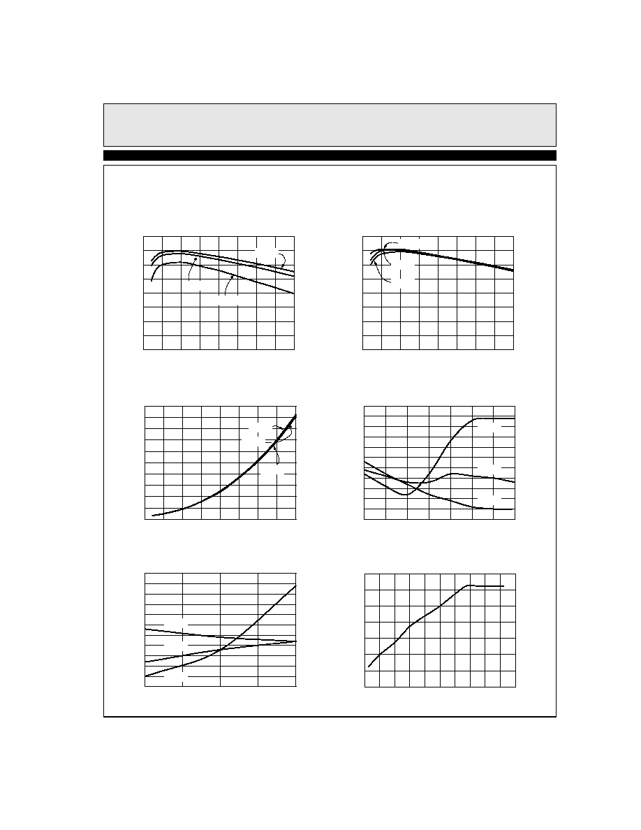
Typical Performance Curves (20-Pin SO Package)
*Power Loss vs I
O
(V
IN
=5V)
2
0
P
o
w
e
r
L
o
s
s
(
W
a
t
t
s
)
0.4
0.8
1.2
1.6
0
4
3.5
3
2.5
2
1
0.5
1.5
Output Current I
O
(A)
V
O
=3.3V
V
O
=2.8V
V
O
=1.8V
0.5
4
3.5
3
2.5
1.5
1
2
Load Current I
O
(A)
Load Regulations (V
O
=3.3V)
3.275
O
u
t
p
u
t
V
o
l
t
a
g
e
(
V
)
3.285
3.295
3.305
3.315
3.325
V
IN
=5V
V
IN
=5.5V
V
IN
=4.5V
Line Regulation (V
O
=3.3V)
3.275
V
O
(
V
)
3.285
3.295
4.5
5.5
5
4.75
5.25
V
IN
(V)
3.325
3.305
3.315
I
O
=0.5A
I
O
=2A
I
O
=4A
V
REF
vs Die Temperature
1.27
1.256
1.268
1.266
1.264
1.262
1.26
1.258
-50
150
-10
30
70
110
Die Temperature (∞C)
V
R
E
F
(
V
)
*Efficiency vs I
O
(V
IN
=5V)
100
60
65
70
75
85
95
0
4
3.5
3
2.5
2
1
0.5
1.5
Load Current I
O
(A)
E
f
f
i
c
i
e
n
c
y
(
%
)
V
O
=3.3V
V
O
=1.8V
0
4
3.5
3
2.5
2
1
0.5
1.5
Load Current I
O
(A)
100
60
65
70
75
95
E
f
f
i
c
i
e
n
c
y
(
%
)
*Efficiency vs I
O
(V
O
=3.3V)
90
80
85
V
IN
=4.5V
V
IN
=5V
V
IN
=5.5V
80
90
V
O
=2.8V
*Note: The 28-Pin HTSSOP Package Offers Improved Performance
6
EL7564C
Monolithic 4 Amp DC:DC Step-down Regulator
E
L
7
5
6
4
C
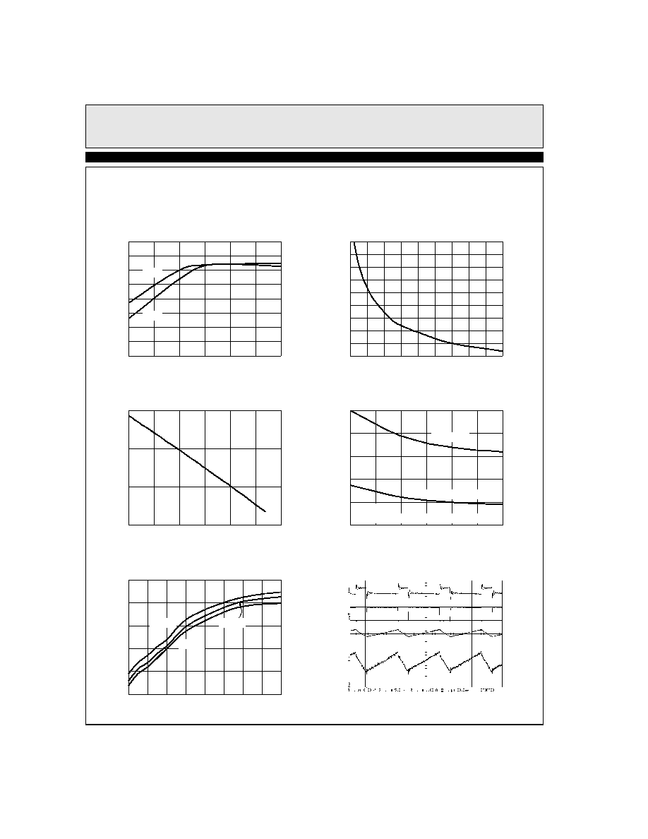
Typical Performance Curves
Oscillator Frequency vs Temperature
360
280
350
340
330
320
310
290
-40
80
-20
20
40
60
Temperature (∞C)
O
s
c
i
l
l
a
t
o
r
F
r
e
q
u
e
n
c
y
(
K
H
z
)
0
300
I
O
=0A
I
O
=4A
Switching Frequency vs C
OSC
1000
100
900
800
700
500
300
200
100
1000
200
400
600
800
C
OSC
(pF)
F
S
(
K
H
z
)
900
300
500
700
600
400
VTJ vs Junction Temperature
1.5
0.9
1.3
1.1
0
150
25
Junction Temperature (∞C)
V
T
J
125
50
75
100
*
JA
vs Copper Area
(20-Pin SO Package)
50
30
46
42
38
34
1
4
1.5
2.5
3.5
PCB Copper Heat-Sinking Area (in
2
)
T
h
e
r
m
a
l
R
e
s
i
s
t
a
n
c
e
(
∞
C
/
W
)
2
3
with no airflow
with 100 LFPM airflow
Switching Waveforms
V
IN
=5V, V
O
=3.3V, I
O
=4A
V
IN
V
LX
i
L
V
O
Chip in the center of copper area
Test Condition:
1 oz. copper PCB used
Current Limit vs T
J
8
3
7
6
5
4
-40
120
-20
40
100
T
J
(∞C)
I
L
M
T
(
A
)
0
80
60
20
V
IN
=4.5V
V
IN
=5.5V
V
IN
=5V
*Note: The 28-Pin HTSSOP Package Offers Improved Performance
7
EL7564C
Monolithic 4 Amp DC:DC Step-down Regulator
E
L
7
5
6
4
C
Typical Performance Curves
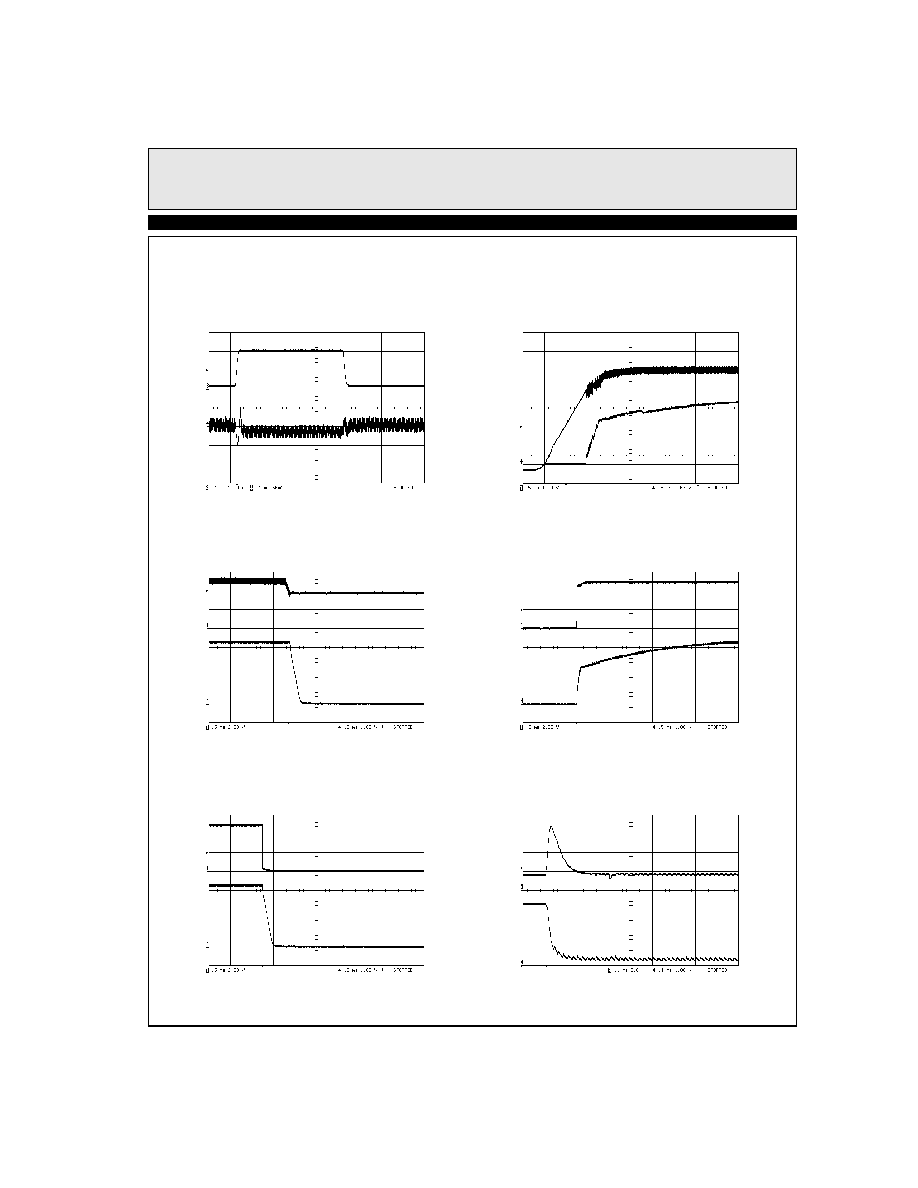
Power-Up
V
IN
=5V, V
O
=3.3V, I
O
=2A
Power-Down
V
IN
=5V, V
O
=3.3V, I
O
=4A
Releasing EN
V
IN
=5V, V
O
=3.3V, I
O
=2A
Shut-Down
V
IN
=5V, V
O
=3.3V, I
O
=4A
Short-Circuit Protection
V
IN
=5V
V
IN
V
O
V
IN
V
O
EN
V
O
EN
V
O
I
O
V
O
Transient Response
V
IN
=5V, V
O
=3.3V, I
O
=0.2A-4A
I
O
V
O
8
EL7564C
Monolithic 4 Amp DC:DC Step-down Regulator
E
L
7
5
6
4
C
Block Diagram
Drivers
PWM
Controller
Power
Tracking
Current
Sense
Junction
Temperature
Voltage
Reference
Oscillator
2.2nF
0.22µF
22
STP
STN
Controller
Supply
SGND
Power
Power
FET
FET
390pF
0.1µF
0.22µF
4.7µH
V
OUT
2370
1k
330µF
VREF
COSC
VHI
VIN
PGND
VDD
VTJ
VDRV
FB
D
1
EN
-
+
PG
VREF
2.2nF

9
EL7564C
Monolithic 4 Amp DC:DC Step-down Regulator
E
L
7
5
6
4
C
Applications Information
Circuit Description
General
The EL7564C is a fixed frequency, current mode con-
trolled DC:DC converter with integrated N-channel
power MOSFETs and a high precision reference. The
device incorporates all the active circuitry required to
implement a cost effective, user-programmable 4A syn-
chronous step-down regulator suitable for use in DSP
core power supplies. By combining fused-lead packag-
ing technology with an efficient synchronous switching
architecture, high power output (13W) can be realized
without the use of discrete external heat sinks.
Theory of Operation
The EL7564C is composed of 7 major blocks:
1. PWM Controller
2. NMOS Power FETs and Drive Circuitry
3. Bandgap Reference
4. Oscillator
5. Temperature Sensor
6. Power Good and Power On Reset
7. Auxiliary Supply Tracking
PWM Controller
The EL7564C regulates output voltage through the use
of current-mode controlled pulse width modulation. The
three main elements in a PWM controller are the feed-
back loop and reference, a pulse width modulator whose
duty cycle is controlled by the feedback error signal, and
a filter which averages the logic level modulator output.
In a step-down (buck) converter, the feedback loop
forces the time-averaged output of the modulator to
equal the desired output voltage. Unlike pure voltage-
mode control systems, current-mode control utilizes
dual feedback loops to provide both output voltage and
inductor current information to the controller. The volt-
age loop minimizes DC and transient errors in the output
voltage by adjusting the PWM duty-cycle in response to
changes in line or load conditions. Since the output volt-
age is equal to the time-averaged of the modulator
output, the relatively large LC time constant found in
power supply applications generally results in low band-
width and poor transient response. By directly
monitoring changes in inductor current via a series sense
resistor the controller's response time is not entirely lim-
ited by the output LC filter and can react more quickly to
changes in line and load conditions. This feed-forward
characteristic also simplifies AC loop compensation
since it adds a zero to the overall loop response. Through
proper selection of the current-feedback to voltage-feed-
back ratio the overall loop response will approach a one-
pole system. The resulting system offers several advan-
tages over traditional voltage control systems, including
simpler loop compensation, pulse by pulse current limit-
ing, rapid response to line variation and good load step
response.
The heart of the controller is an input direct summing
comparator which sum voltage feedback, current feed-
back, slope compensation ramp and power tracking
signals together. Slope compensation is required to pre-
vent system instability that occurs in current-mode
topologies operating at duty-cycles greater than 50%
and is also used to define the open-loop gain of the over-
all system. The slope compensation is fixed internally
and optimized for 500mA inductor ripple current. The
power tracking will not contribute any input to the com-
parator steady-state operation. Current feedback is
measured by the patented sensing scheme that senses the
inductor current flowing through the high-side switch
whenever it is conducting. At the beginning of each
oscillator period the high-side NMOS switch is turned
on. The comparator inputs are gated off for a minimum
period of time of about 150ns (LEB) after the high-side
switch is turned on to allow the system to settle. The
Leading Edge Blanking (LEB) period prevents the
detection of erroneous voltages at the comparator inputs
due to switching noise. If the inductor current exceeds
the maximum current limit (ILMAX) a secondary over-
current comparator will terminate the high-side switch
on time. If ILMAX has not been reached, the feedback
voltage FB derived from the regulator output voltage
VOUT is then compared to the internal feedback refer-
ence voltage. The resultant error voltage is summed with
the current feedback and slope compensation ramp. The
10
EL7564C
Monolithic 4 Amp DC:DC Step-down Regulator
E
L
7
5
6
4
C
high-side switch remains on until all four comparator
inputs have summed to zero, at which time the high-side
switch is turned off and the low-side switch is turned on.
However, the maximum on-duty ratio of the high-side
switch is limited to 95%. In order to eliminate cross-con-
duction of the high-side and low-side switches a 15ns
break-before-make delay is incorporated in the switch
drive circuitry. The output enable (EN) input allows the
regulator output to be disabled by an external logic con-
trol signal.
Output Voltage Setting
In general:
However, due to the relatively low open loop gain of the
system, gain errors will occur as the output voltage and
loop-gain is changed. This is shown in the performance
curves. A 100nA pull-up current from FB to VDD forces
VOUT to GND in the event that FB is floating.
NMOS Power FETs and Drive Circuitry
The EL7564C integrates low on-resistance (30m
)
NMOS FETs to achieve high efficiency at 4A. In order
to use an NMOS switch for the high-side drive it is nec-
essary to drive the gate voltage above the source voltage
(LX). This is accomplished by bootstrapping the VHI
pin above the LX voltage with an external capacitor
CVHI and internal switch and diode. When the low-side
switch is turned on and the LX voltage is close to GND
potential, capacitor CVHI is charged through internal
switch to VDRV, typically 5V. At the beginning of the
next cycle the high-side switch turns on and the LX pins
begin to rise from GND to VIN potential. As the LX pin
rises the positive plate of capacitor CVHI follows and
eventually reaches a value of VDRV+VIN, typically
10V, for VDRV=VIN=5V. This voltage is then level
shifted and used to drive the gate of the high-side FET,
via the VHI pin. A value of 0.22µF for CVHI is
recommended.
Reference
A 1.5% temperature compensated bandgap reference is
integrated in the EL7564C. The external VREF capaci-
tor acts as the dominant pole of the amplifier and can be
increased in size to maximize transient noise rejection.
A value of 0.1µF is recommended.
Oscillator
The system clock is generated by an internal relaxation
oscillator with a maximum duty-cycle of approximately
95%. Operating frequency can be adjusted through the
COSC pin or can be driven by an external source. If the
oscillator is driven by an external source care must be
taken in selecting the ramp amplitude. Since CSLOPE
value is derived from the COSC ramp, changes to COSC
ramp will change the CSLOPE compensation ramp
which determine the open-loop gain of the system.
When external synchronization is required, always
choose C
OSC
such that the free-running frequency is at
least 20% lower than that of sync source to accommo-
date component and temperature variations. Figure 1
shows a typical connection.
Junction Temperature Sensor
An internal temperature sensor continuously monitors
die temperature. In the event that die temperature
exceeds the thermal trip-point, the system is in fault state
and will be shut down. The upper and low trip-points are
set to 135∞C and 115∞C respectively.
The VTJ pin is an accurate indication of the internal sili-
con junction temperature (see performance curve.) The
VOUT
0.975V
1
R2
R1
------
+
◊
=
2
3
16
15
14
13
5
6
7
12
11
9
8
10
19
18
EL7564C
1
20
External
Oscillator
BAT54S
100pF
390pF
Figure 1. Oscillator Synchronization
11
EL7564C
Monolithic 4 Amp DC:DC Step-down Regulator
E
L
7
5
6
4
C
junction temperature T
J
(∞C) can be deducted from the
following relation:
Where VTJ is the voltage at VTJ pin in volts.
Power Good and Power On Reset
During power up the output regulator will be disabled
until VIN reaches a value of approximately 4V. About
500mV hysteresis is present to eliminate noise-induced
oscillations.
Under-voltage and over-voltage conditions on the regu-
lator output are detected through an internal window
comparator. A logic high on the PG output indicates that
the regulated output voltage is within about +10% of the
nominal selected output voltage.
Power Tracking
The power tracking pins STP and STN are the inputs to
a comparator, whose HI output forces the PWM control-
ler to skip switching cycle.
1. Linear Tracking
In this application, it is always the case that the lower
voltage supply V
C
tracks the higher output supply V
P
.
Please see Figure 2 below.
TJ
75
1.2 VTJ
≠
0.00384
------------------------
+
=
Figure 2. Linear Power Tracking
1
2
15
14
13
12
6
7
8
11
10
9
20
19
EL7564C
-
+
1
2
15
14
13
12
6
7
8
11
10
9
20
19
EL7564C
-
+
V
C
V
P
V
OUT
TIME
V
C
V
P
12
EL7564C
Monolithic 4 Amp DC:DC Step-down Regulator
E
L
7
5
6
4
C
2. Offset Tracking
The intended start-up sequence is shown in Figure 3a. In
this configuration, V
C
will not start until V
P
reaches a
preset value of:
However, due to the superimpose of V
C
and V
IN
, the
choice of R
A
and R
B
are restricted by the following
relationship:
Where 0.5 is for noise immunity. See Figure 3 below.
R
B
R
A
R
B
+
-------------------- V
IN
◊
V
P
0.5
R
B
R
A
R
B
+
-------------------- V
IN
R
A
R
A
R
B
+
--------------------
+
◊
V
C
◊
<
+
Figure 3. Offset Power Tracking
V
OUT
TIME
V
C
V
P
1
2
15
14
13
12
6
7
8
11
10
9
20
19
EL7564C
-
+
1
2
15
14
13
12
6
7
8
11
10
9
20
19
EL7564C
-
+
V
C
V
P
STP
STN
STP
STN
V
IN
R
A
R
B
13
EL7564C
Monolithic 4 Amp DC:DC Step-down Regulator
E
L
7
5
6
4
C
The second way of offset tracking is to use the EN and
Power Good pins, as shown in Figure 4. In this configu-
ration, V
P
does not have to be larger than V
C
.
Figure 4. Offset Tracking
V
C
2
3
16
15
14
13
5
6
7
12
11
9
8
10
19
18
EL7564C
2
3
16
15
14
13
5
6
7
12
11
9
8
10
19
18
EL7564C
1
20
1
20
V
P
EN
PG
EN
PG
TIME
V
C
V
P
14
EL7564C
Monolithic 4 Amp DC:DC Step-down Regulator
E
L
7
5
6
4
C
3. External Soft Start
An external soft start can be combined with auxilliary
supply tracking to provide desired soft start other than
internally preset soft start (Figure 5). The appropriate
start-up time is:
ts
R C
VO
VIN
---------
◊
◊
=
Figure 5. External Soft Start
1
2
15
14
13
12
6
7
8
11
10
9
20
19
EL7564C
-
+
V
OUT
STP
STN
V
IN
R
C
15
EL7564C
Monolithic 4 Amp DC:DC Step-down Regulator
E
L
7
5
6
4
C
4. Start-up Delay
A capacitor can be added to the EN pin to delay the con-
verter start-up (Figure 6) by utilizing the pull-up current.
The delay time is approximately:
td ms
(
)
1200 C
µ
F
(
)
◊
=
Figure 6. Start-up Delay
1
2
15
14
13
12
6
7
8
11
10
9
20
19
EL7564C
-
+
V
OUT
STP
STN
C
TIME
V
O
V
IN
t
d
16
EL7564C
Monolithic 4 Amp DC:DC Step-down Regulator
E
L
7
5
6
4
C
Thermal Management
The EL7564CM utilizes "fused lead" packaging tech-
nology in conjunction with the system board layout to
achieve a lower thermal resistance than typically found
in standard SO20 packages. By fusing (or connecting)
multiple external leads to the die substrate within the
package, a very conductive heat path is created to the
outside of the package. This conductive heat path MUST
then be connected to a heat sinking area on the PCB in
order to dissipate heat out and away from the device.
The conductive paths for the EL7564CM package are
the fused leads: # 6, 7, 11, 12, and 13. If a sufficient
amount of PCB metal area is connected to the fused
package leads, a junction-to-ambient resistance of
43∞C/W can be achieved (compared to 85∞C/W for a
standard SO20 package). The general relationship
between PCB heat-sinking metal area and the thermal
resistance for this package is shown in the Performance
Curves section of this data sheet. It can be readily seen
that the thermal resistance for this package approaches
an asymptotic value of approximately 43∞C/W without
any airflow, and 33∞C/W with 100 LFPM airflow. Addi-
tional information can be found in Application Note #8
(Measuring the Thermal Resistance of Power Surface-
Mount Packages). For a thermal shutdown die junction
temperature of 135∞C, and power dissipation of 1.5W,
the ambient temperature can be as high as 70∞C without
airflow. With 100 LFPM airflow, the ambient tempera-
ture can be extended to 85∞C.
The EL7564CRE utilizes the 28-pin HTSSOP package.
The majority of heat is dissipated through the heat pad
exposed at the bottom of the package. Therefore, the
heat pad needs to be soldered to the PCB. The thermal
resistance for this package is better than that of SO20.
Actual test results are available from Elantec Applica-
tions staff. The actual junction temperature can be
measured at VTJ pin.
Since the thermal performance of the IC is heavily
dependent on the board layout, the system designer
should exercise care during the design phase to ensure
that the IC will operate under the worst-case environ-
mental conditions.
Layout Considerations
The layout is very important for the converter to func-
tion properly. Power Ground ( ) and Signal Ground (
---
)
should be separated to ensure that the high pulse current
in the Power Ground never interferes with the sensitive
signals connected to Signal Ground. They should only
be connected at one point (normally at the negative side
of either the input or output capacitor.)
The trace connected to the FB pin is the most sensitive
trace. It needs to be as short as possible and in a "quiet"
place, preferably between PGND or SGND traces.
In addition, the bypass capacitor connected to the VDD
pin needs to be as close to the pin as possible.
The heat of the chip is mainly dissipated through the
PGND pins. Maximizing the copper area around these
pins is preferable. In addition, a solid ground plane is
always helpful for the EMI performance.
The demo board is a good example of layout based on
these principles. Please refer to the EL7564C Applica-
tion Brief for the layout.
17
EL7564C
Monolithic 4 Amp DC:DC Step-down Regulator
E
L
7
5
6
4
C
Package Outline Drawing (20-Pin SO Package)
NOTE: The package drawing shown here may not be the latest version. For the latest revision, please refer to the
Elantec website at http://www.elantec.com/pages/package_outline.html
18
EL7564C
Monolithic 4 Amp DC:DC Step-down Regulator
E
L
7
5
6
4
C
General Disclaimer
Specifications contained in this data sheet are in effect as of the publication date shown. Elantec, Inc. reserves the right to make changes in the cir-
cuitry or specifications contained herein at any time without notice. Elantec, Inc. assumes no responsibility for the use of any circuits described
herein and makes no representations that they are free from patent infringement.
WARNING - Life Support Policy
Elantec, Inc. products are not authorized for and should not be used
within Life Support Systems without the specific written consent of
Elantec, Inc. Life Support systems are equipment intended to sup-
port or sustain life and whose failure to perform when properly used
in accordance with instructions provided can be reasonably
expected to result in significant personal injury or death. Users con-
templating application of Elantec, Inc. Products in Life Support
Systems are requested to contact Elantec, Inc. factory headquarters
to establish suitable terms & conditions for these applications. Elan-
tec, Inc.'s warranty is limited to replacement of defective
components and does not cover injury to persons or property or
other consequential damages.
O
c
t
o
b
e
r
3
,
2
0
0
1
Printed in U.S.A.
Elantec Semiconductor, Inc.
675 Trade Zone Blvd.
Milpitas, CA 95035
Telephone: (408) 945-1323
(888) ELANTEC
Fax:
(408) 945-9305
European Office: +44-118-977-6020
Japan Technical Center: +81-45-682-5820