EL7501C
January
1996
Rev
B
EL7501C
100V High Side Driver
Note All information contained in this data sheet has been carefully checked and is believed to be accurate as of the date of publication however this data sheet cannot be a ``controlled document'' Current revisions if any to these
specifications are maintained at the factory and are available upon your request We recommend checking the revision level before finalization of your design documentation
1994 Elantec Inc
Features
100V High Side Voltage
Rail to Rail Output
1 MHz Operation
1 0A Peak Current
Matched Rise and Fall Times
Direct Coupled
No Start Up Ambiguity
Applications
Uninterruptible Power Supplies
DC-DC Converters
Motor Control
Power MOSFET Driver
Ordering Information
Part No
Temp Range
Package
Outline
EL7501CN
b
40 C to
a
85 C 8-Pin P-Dip
MDP0031
EL7501CS
b
40 C to
a
85 C 8-Lead SO
MDP0027
General Description
The EL7501 provides a low cost solution to many high side
drive applications The EL7501 is DC coupled so there are no
start up problems associated with AC coupled schemes The
EL7501 is driven by user supplied complementary signals
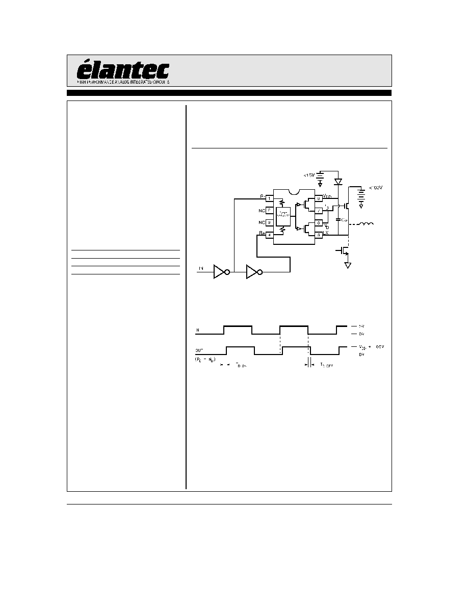
Connection Diagram
7501 1
Figure 1
7501 Waveform Example
7501 6
EL7501C
100V High Side Driver
Absolute Maximum Ratings
(T
A
e
25 C)
Supply (V
DD
or LX to R
b
or R
a
)
100V
Supply (V
DD
to LX)
16 5V
Output Pins
b
0 3V below GND
a
0 3V above V
DD
Peak Output Current
2A
Ambient Operating Temperature
b
40 C to
a
85 C
Storage Temperature Range
b
65 C to
a
150 C
Operating Junction Temperature
125 C
Power Dissipation
SOIC
570 mW
PDIP
1050 mW
Important Note
All parameters having Min Max specifications are guaranteed The Test Level column indicates the specific device testing actually
performed during production and Quality inspection Elantec performs most electrical tests using modern high-speed automatic test
equipment specifically the LTX77 Series system Unless otherwise noted all tests are pulsed tests therefore T
J
e
T
C
e
T
A
Test Level
Test Procedure
I
100% production tested and QA sample tested per QA test plan QCX0002
II
100% production tested at T
A
e
25 C and QA sample tested at T
A
e
25 C
T
MAX
and T
MIN
per QA test plan QCX0002
III
QA sample tested per QA test plan QCX0002
IV
Parameter is guaranteed (but not tested) by Design and Characterization Data
V
Parameter is typical value at T
A
e
25 C for information purposes only
DC Electrical Characteristics
(T
A
e
25 C V
DD
e
15V C
LOAD
e
1000 pF unless otherwise specified)
Parameter
Description
Test Conditions
Min
Typ
Max
Test
Units
Level
Input Output
V
DIFF (Min)
Minimum Differential Input
1 0
I
V
Signal to Switch Output
I
DS OFF
Output Leakage
GND
k
V
OUT
k
V
DD
b
10 0
0 2
a
10 0
I
mA
R
OH
Pull-up Resistance
I
OUT
e b
100 mA
5 0
10 0
I
X
R
OL
Pull-down Resistance
I
OUT
e a
100 mA
5 0
10 0
I
X
I
PK
Peak Output Current
1 0
IV
A
I
DC
Continuous Output
50 0
IV
mA
Current Source Sink
Power Supply
I
DD
Supply Current
4 0
I
mA
into V
DD
V
DD
Operating Voltage
4 5
15 0
I
V
2
TD
is
27in
EL7501C
100V High Side Driver
AC Electrical Characteristics
(T
A
e
25 C V
DD
e
15V C
LOAD
e
1000 pF unless otherwise specified)
Parameter
Description
Test Conditions
Min
Typ
Max
Test
Units
Level
Switching Characteristics
t
R
Rise Time
C
L
e
500 pF
15 0
IV
ns
C
L
e
1000 pF
20 0
40 0
t
F
Fall Time
C
L
e
500 pF
15 0
IV
ns
C
L
e
1000 pF
20 0
40 0
t
D OFF
Turn Off
90 0
140 0
IV
ns
Delay Time
t
D ON
Turn On
90 0
140 0
IV
ns
Delay Time
7501-2
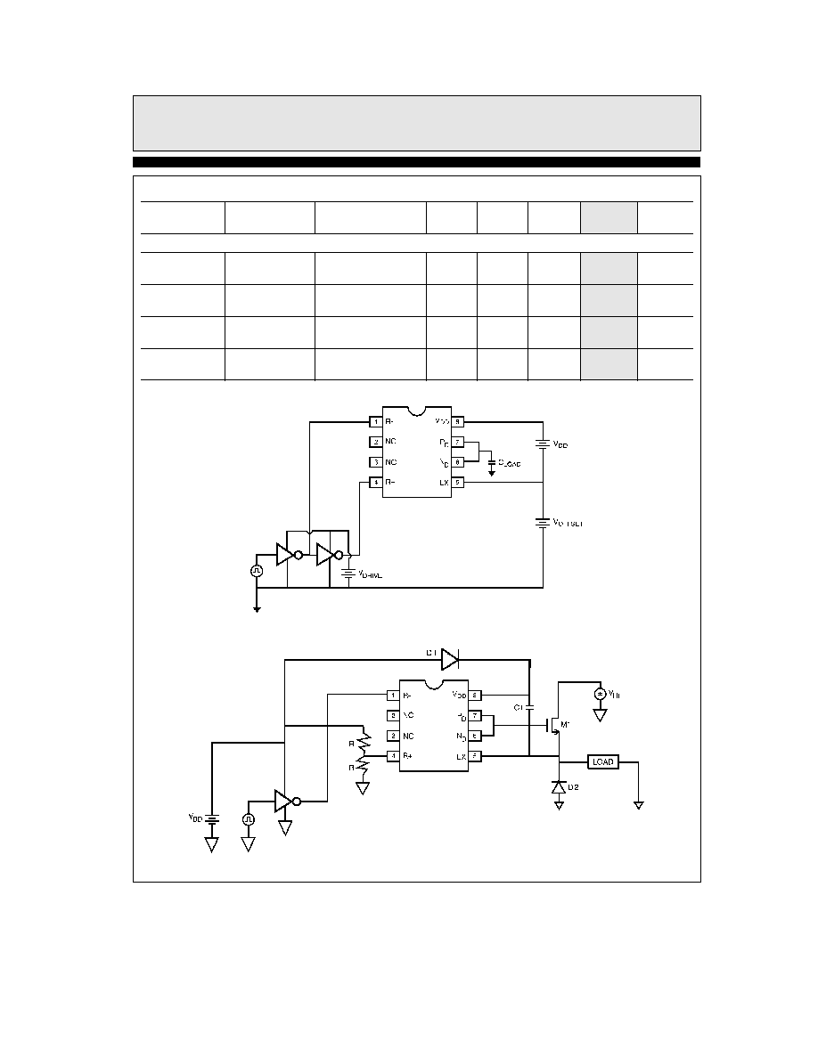
Figure 2 EL7501 Test Circuit
7501-3
Figure 3 EL7501 Alternate Drive Method
3
TD
is
19in
EL7501C
100V High Side Driver
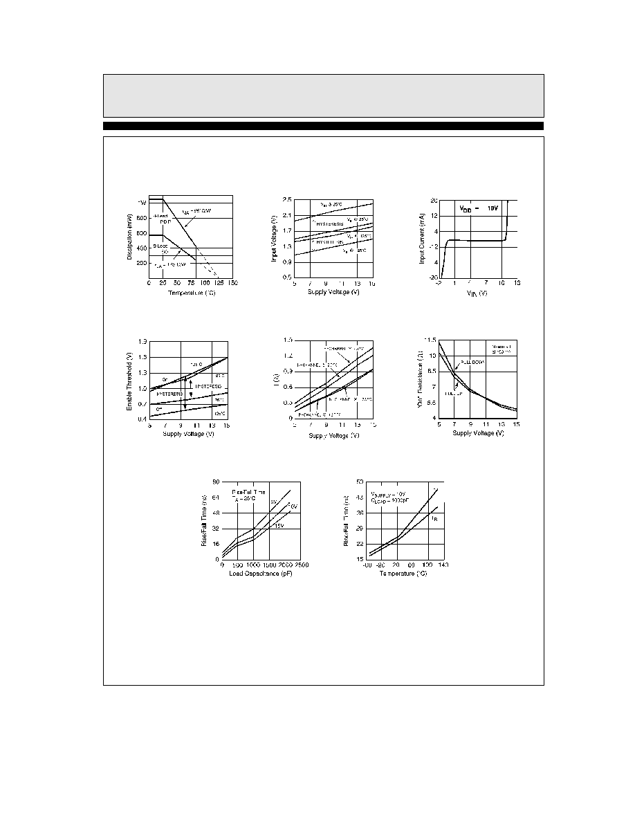
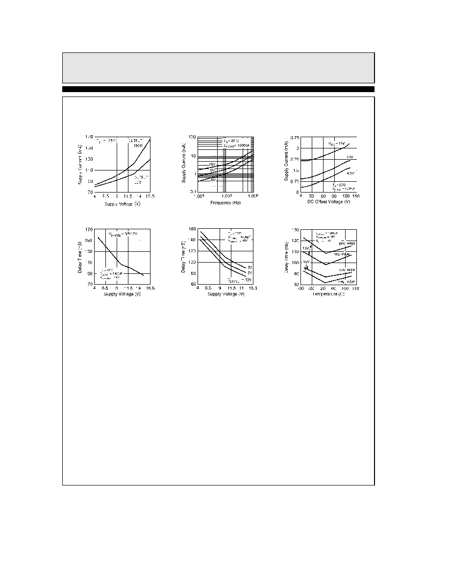
Typical Performance Curves
vs Supply Voltage
Quiescent Supply Current
and Frequency
Current vs Voltage
Average Supply
and V
DD
DC Offset Voltage
Supply Current vs
Voltage and Drive Voltage
Delay Time vs Supply
Output Rising Edge
Voltage and Drive Voltage
Delay Time vs Supply
Output Falling Edge
Supply Voltage
Temperature and
Delay Time vs
7501-4
4