 | –≠–ª–µ–∫—Ç—Ä–æ–Ω–Ω—ã–π –∫–æ–º–ø–æ–Ω–µ–Ω—Ç: EL7551CU | –°–∫–∞—á–∞—Ç—å:  PDF PDF  ZIP ZIP |
Note: All information contained in this data sheet has been carefully checked and is believed to be accurate as of the date of publication; however, this data sheet cannot be a "controlled document". Current revisions, if any, to these
specifications are maintained at the factory and are available upon your request. We recommend checking the revision level before finalization of your design documentation.
© 2001 Elantec Semiconductor, Inc.
E
L
7
5
5
1
C
-
P
r
e
l
i
m
i
n
a
r
y
General Description
The EL7551C is an integrated, synchronous step-down regulator with
output voltage adjustable from 1.0V to 3.8V. It is capable of delivering
1A continuous current at up to 95% efficiency. The EL7551C operates
at a constant frequency pulse width modulation (PWM) mode, making
external synchronization possible. Patented on-chip resistorless cur-
rent sensing enables current mode control, which provides cycle-by-
cycle current limiting, over-current protection, and excellent step load
response. The EL7551C is available in a fused-lead 16-pin QSOP
package. With proper external components, the whole converter fits
into a less than 0.4 in
2
area. The minimal external components and
small size make this EL7551C ideal for desktop and portable
applications.
The EL7551C is specified for operation over the -40∞C to +85∞C tem-
perature range.
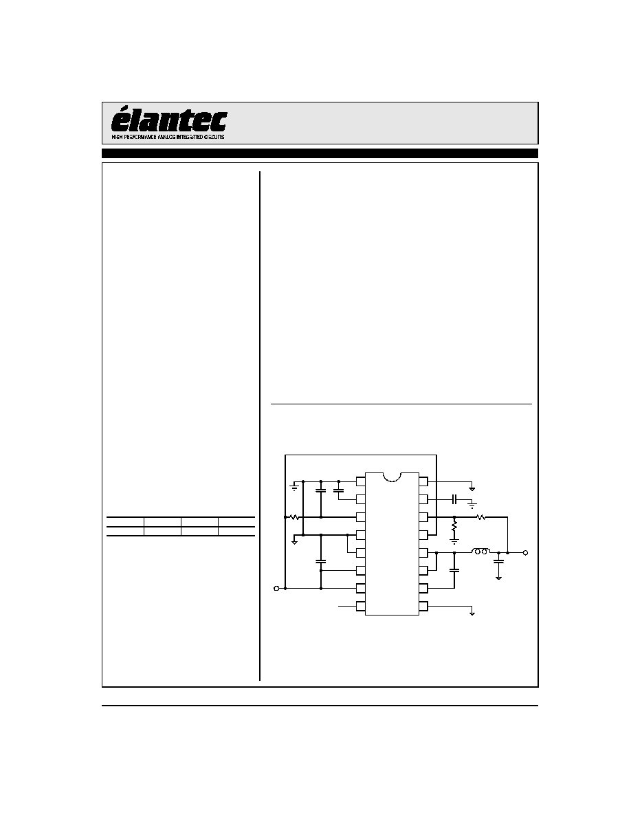
Typical Application Diagram
Manufactured under U.S. Patent No. 57,323,974
1
2
3
4
16
15
14
13
5
6
7
12
11
10
8
9
SGND
COSC
VDD
PGND
PGND
VIN
VIN
EN
PGND
VREF
FB
VDRV
LX
LX
VHI
PGND
R3
R2
L1
C3
C4
C1
C5
R1
C6
C
7
V
O
(3.3V,
1A)
V
IN
(4.5V-
5.5V)
2.37k
10µH
1k
0.1µF
47µF
0.1µF
0.1µF 270pF
39
10µF
ceramic
EL7551C
Features
∑ Integrated synchronous MOSFETs
and current mode controller
∑ 1A continuous output current
∑ Up to 95% efficiency
∑ 4.5V to 5.5V input voltage
∑ Adjustable output from 1V to 3.8V
∑ Cycle-by-cycle current limit
∑ Precision reference
∑ ±0.5% load and line regulation
∑ Adjustable switching frequency to
1MHz
∑ Oscillator synchronization
possible
∑ Internal soft start
∑ Over temperature protection
∑ Under voltage lockout
∑ 16-pin QSOP package
Applications
∑ DSP, CPU Core and IO Supplies
∑ Logic/Bus Supplies
∑ Portable Equipment
∑ DC:DC Converter Modules
∑ GTL + Bus Power Supply
Ordering Information
Part No
Package
Tape & Reel
Outline #
EL7551CU
16-Pin QSOP
MDP0040
EL7551C - Preliminary
Monolithic 1 Amp DC:DC Step-down Regulator
O
c
t
o
b
e
r
3
,
2
0
0
1
2
EL7551C - Preliminary
Monolithic 1 Amp DC:DC Step-down Regulator
E
L
7
5
5
1
C
-
P
r
e
l
i
m
i
n
a
r
y
Absolute Maximum Ratings
(T
A
= 25∞C)
Supply Voltage between V
IN
or V
DD
and GND
+6.5V
V
LX
Voltage
V
IN
+0.3V
Input Voltage
GND -0.3V, V
DD
+0.3V
V
HI
Voltage
GND -0.3V, V
LX
+6V
Storage Temperature
-65∞C to +150∞C
Operating Ambient Temperature
-40∞C to +85∞C
Operating Junction Temperature
+135∞C
Important Note:
All parameters having Min/Max specifications are guaranteed. Typ values are for information purposes only. Unless otherwise noted, all tests are at the
specified temperature and are pulsed tests, therefore: T
J
= T
C
= T
A
.
DC Characteristics
V
DD
= V
IN
= 5V, T
A
= T
J
= 25∞C, C
OSC
= 1.2nF, unless otherwise specified.
Parameter
Description
Conditions
Min
Typ
Max
Unit
V
REF
Reference Accuracy
1.24
1.26
1.28
V
V
REFTC
Reference Temperature Coefficient
50
ppm/∞C
V
REFLOAD
Reference Load Regulation
0 < I
REF
< 50µA
-1
%
V
RAMP
Oscillator Ramp Amplitude
1.15
V
I
OSC_CHG
Oscillator Charge Current
0.1V < V
OSC
< 1.25V
200
µA
I
OSC_DIS
Oscillator Discharge Current
0.1V < V
OSC
< 1.25V
8
mA
I
VDD
+V
DRV
V
DD
+V
DRV
Supply Current
V
EN
= 4V, F
OSC
= 120kHz
3.5
5
mA
I
VDD_OFF
V
DD
Standby Current
EN = 0
1
1.5
mA
V
DD_OFF
V
DD
for Shutdown
3.5
4
V
V
DD_ON
V
DD
for Startup
3.95
4.45
V
T
OT
Over Temperature Threshold
135
∞C
T
HYS
Over Temperature Hysteresis
20
∞C
I
LEAK
Internal FET Leakage Current
EN = 0, L
X
= 5V (low FET), L
X
= 0V (high FET)
10
µA
I
LMAX
Peak Current Limit
2
A
R
DSON
FET On Resistance
Wafer level test only
45
95
m
R
DSONTC
R
DSON
Tempco
0.2
m
/∞C
V
FB
Output Initial Accuracy
I
LOAD
= 0A
0.960
0.975
0.99
V
V
FB_LINE
Output Line Regulation
V
IN
= 5V,
V
IN
= 10%, I
LOAD
= 0A
0.5
%
V
FB_LOAD
Output Load Regulation
0.1A < I
LOAD
< 1A
0.5
%
V
FB_TC
Output Temperature Stability
-40∞C < T
A
< 85∞C, I
LOAD
= 0.5A
±1
%
I
FB
Feedback Input Pull Up Current
V
FB
= 0V
100
200
nA
V
EN_HI
EN Input High Level
3.2
4
V
V
EN_LO
EN Input Low Level
1
V
I
EN
Enable Pull Up Current
V
EN
= 0
-4
-2.5
µA
Closed Loop AC Electrical Characteristics
V
S
= V
IN
= 5V, T
A
= T
J
= 25∞C, C
OSC
= 1.2nF, unless otherwise specified.
Parameter
Description
Conditions
Min
Typ
Max
Unit
F
OSC
Oscillator Initial Accuracy
105
117
130
kHz
t
SYNC
Minimum Oscillator Sync Width
25
ns
M
SS
Soft Start Slope
0.5
V/ms
t
BRM
FET Break Before Make Delay
15
ns
t
LEB
High Side FET Minimum On Time
150
ns
D
MAX
Maximum Duty Cycle
95
%
3
EL7551C - Preliminary
Monolithic 1 Amp DC:DC Step-down Regulator
E
L
7
5
5
1
C
-
P
r
e
l
i
m
i
n
a
r
y
Pin Descriptions
Pin Number
Pin Name
Pin Function
1
SGND
Control circuit negative supply.
2
COSC
Oscillator timing capacitor. FOSC can be approximated by: FOSC (kHz) = 0.1843/COSC, COSC in µF.
3
VDD
Control circuit positive supply.
4
PGND
Ground return of the regulator. Connected to the source of the low-side synchronous NMOS power FET.
5
PGND
Ground return of the regulator. Connected to the source of the low-side synchronous NMOS power FET.
6
VIN
Power supply input of the regulator. Connected to the drain of the high-side NMOS power FET.
7
VIN
Power supply input of the regulator. Connected to the drain of the high-side NMOS power FET.
8
EN
Chip Enable, active high. A 2µA internal pull-up current enables the device if the pin is left open.
9
PGND
Ground return of the regulator.
10
VHI
Positive supply of the high-side driver.
11
LX
Inductor drive pin. High current digital output whose average voltage equals the regulator output voltage.
12
LX
Inductor drive pin. High current digital output whose average voltage equals the regulator output voltage.
13
VDRV
Positive supply of the low-side driver and input voltage for the high-side boot strap.
14
FB
Voltage feedback input. Connected to an external resistor divider between VOUT and GND. A 125nA pull-up current
forces VOUT to VS in the event that FB is floating.
15
VREF
Bandgap reference bypass capacitor. Typically 0.1µF to GND.
16
PGND
Ground return of the regulator.
4
EL7551C - Preliminary
Monolithic 1 Amp DC:DC Step-down Regulator
E
L
7
5
5
1
C
-
P
r
e
l
i
m
i
n
a
r
y
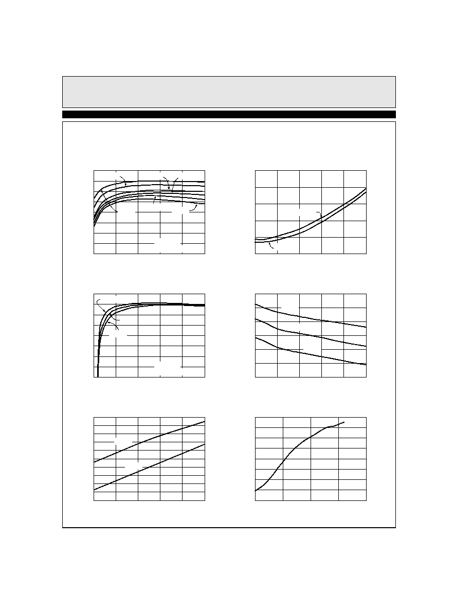
Typical Performance Curves
Efficiency vs I
O
V
IN
=5V
100
95
90
85
80
75
70
65
60
0.1
0.2
0.4
0.6
1
Load Current I
O
(A)
E
f
f
i
c
i
e
n
c
y
(
%
)
V
O
=3.3V
V
O
=1.8V
V
O
=1.2V
V
O
=1V
V
O
=2.5V
Power Loss vs I
O
V
IN
=5V
0.25
0.2
0.15
0.1
0.05
0
0
0.2
0.4
0.8
1
Output Current I
O
(A)
P
o
w
e
r
L
o
s
s
(
W
)
Load Regulation
V
O
=3.3V
0.6
0.4
0
-0.2
-0.4
-0.6
0
0.2
0.4
0.8
1
Load Current I
O
(A)
O
u
t
p
u
t
V
o
l
t
a
g
e
(
%
)
V
REF
vs Temperature
1.258
1.256
1.254
1.252
1.25
1.248
1.246
1.244
1.242
-40
10
60
110
160
Temperature (∞C)
V
R
E
F
(
V
)
Efficiency vs I
O
V
O
=3.3V
100
95
90
85
80
75
70
65
60
0
0.2
0.4
0.6
1
Load Current I
O
(A)
E
f
f
i
c
i
e
n
c
y
(
%
)
Line Regulation
V
O
=3.3V
0.6
0.5
0.4
0.2
0
-0.2
-0.4
4.5
4.7
5.1
5.3
5.5
V
IN
(V)
V
O
(
%
)
V
IN
=4.5V
V
IN
=5V
V
IN
=5.5V
V
IN
=4.5V
V
IN
=5V
V
IN
=5.5V
4.9
I
O
=0.1A
I
O
=1A
V
O
=1.5V
V
O
=3.3V
V
O
=1V
0.6
0.8
0.6
0.2
0.3
0.1
-0.1
-0.3
0.8
F
S
=500kHz
L=Coilcraft DO3316P-472
F
S
=500kHz
L=Coilcraft DO3316P-472
5
EL7551C - Preliminary
Monolithic 1 Amp DC:DC Step-down Regulator
E
L
7
5
5
1
C
-
P
r
e
l
i
m
i
n
a
r
y
Typical Performance Curves
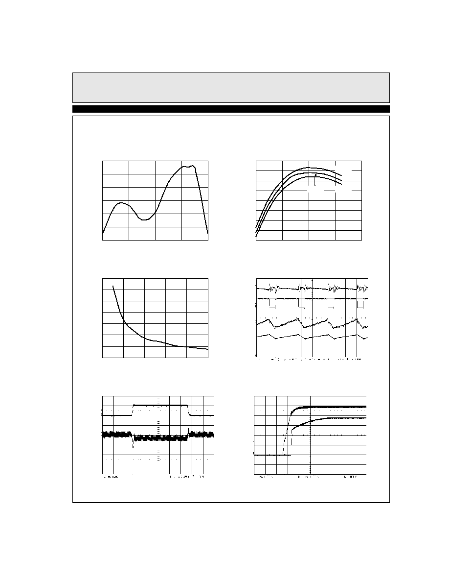
Switching Waveforms
V
IN
=5V, V
O
=3.8V, I
O
=1A
V
I
V
LX
V
O
i
L
Power-Up
V
IN
=5V, V
O
=3.8V, I
O
=1A
Transient Response
V
IN
=5V, V
O
=3.8V, I
O
=0A-1A
i
O
V
O
V
IN
V
O
Oscillator Frequency vs Temperature
390
385
380
375
370
365
360
-40
0
40
80
120
Temperature (∞C)
O
s
c
i
l
l
a
t
o
r
F
r
e
q
u
e
n
c
y
(
k
H
z
)
Input Current vs Temperature
(Enable connected to GND)
0.96
0.94
0.92
0.88
0.86
0.84
0.82
0.8
-40
10
60
110
160
Temperature (∞C)
I
n
p
u
t
C
u
r
r
e
n
t
(
m
A
)
Switching Frequency vs C
OSC
1400
1200
1000
800
600
400
200
0
0
400
600
800
1000
C
OSC
(pF)
F
S
(
k
H
z
)
0.9
V
IN
=4.5V
V
IN
=5V
V
IN
=5.5V
200