 | –≠–ª–µ–∫—Ç—Ä–æ–Ω–Ω—ã–π –∫–æ–º–ø–æ–Ω–µ–Ω—Ç: EL7556C | –°–∫–∞—á–∞—Ç—å:  PDF PDF  ZIP ZIP |

EL7556C
Adjustable CPU Power Supply Unit
1
Features
∑
6 Amps Continuous Load Current
∑
Precision Internal 1% Reference
∑
1.0V to 3.8V Output Voltage
∑
Internal Power MOSFETs
∑
>90% Efficiency
∑
Synchronous Switching
∑
Adjustable Slope Compensation
∑
Over Temperature Indicator
∑
Pulse by Pulse Current Limiting
∑
Operates up to 1MHz
∑
1.5% Typical Output Accuracy
∑
Adjustable Oscillator w/Sync
∑
Remote Enable/Disable
∑
Intel P54 and P55 Compatible
∑
VCC2DET Interface
∑
Internal Soft Start
Applications
∑
PC Motherboards
∑
Local High Power CPU Supplies
∑
5V to 1.0V DC-DC Conversion
∑
Portable Electronics/Instruments
∑
P54 and P55 Regulators
∑
GTL+ Bus Power Supply
Ordering Information
Part No.
Temp. Range
Package
Outline #
EL7556CM
0oC to 70oC
28-Pin SOIC MDP0027
General Description
The EL7556C is an adjustable synchronous DC:DC switching
regulator optimized for a 5V input and 1.0-3.8V output. By
combining integrated NMOS power FETS with fused-lead
packaging the EL7556 can supply up to 6A continuous output
current without the use of external power devices or discrete
heat sinks, thereby minimizing design effort and overall
system cost.
On chip resistorless current sensing is used to achieve stable,
highly efficient, current-mode control. The EL7556 also
incorporates the VCC2DET function to directly interface with
the Intel P54 and P55 microprocessors. Depending on the state
of VCC2DET the output voltage is internally preset to 3.50V
or a user-adjustable voltage using two external resistors. In
both internal and external feedback modes the active-high
PWRGD output indicates when the regulator output is within
+/-10% of the programmed voltage. An on-board sensor
monitors die temperature (OT) for over-temperature
conditions and can be connected directly to OUTEN to
provide automatic thermal shutdown. Adjustable oscillator
frequency and slope compensation allow added flexibility in
overall system design
.
EL7556C
Adjustable CPU Power Supply Unit
2
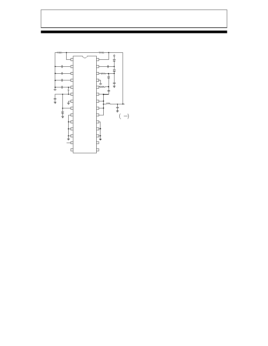
Connection Diagram
Fig 1.
VSSP
VIN
VSSP
VIN
LX
LX
FB2
LX
C
SLOPE
C
REF
C
OSC
CP
C2V
VSS
VSSP
VSSP
VCC2DET
OUTEN
OT
PWRGD
VSSP
VSSP
FB1
+
1.0V-3.8V
-
TEST
VSSP
LX
VHI
VDD
28
27
26
25
1
2
24
23
22
21
3
4
5
6
7
8
9
20
19
18
17
16
15
14
13
12
11
10
5V
.1uF
100pF
220pF
1mF
+
10V
-
C5
1uF
1uF
C11
L1
2.5uH
1mF
C10
.1uF
C6
C9
C8
C7
C4
D1
D2
R1
100
V
O
= 1.0
1 + R3
R4
R4
100
R3
150
D3
VDD
R6
22
C3
.1uF
R5
10
- +
L1: Pulse Engineering PE-53681
C9: 3X330uF
C10: 3X330uF
(Sprague 594D337X10010R2T)
D1-D3: BAV99 fast diode
Connect to VSSP for
external feedback
AGND
AGND and PGND should be
connected at C10.
PGND

EL7556C
Adjustable CPU Power Supply Unit
3
Absolute Maximum Ratings
(T
A
= 25
∞
C)
Storage Temperature Range
-65∞C to +150∞C
Supply (V
IN
)
5.5V
Ambient Operating Temperature
0∞C to +70∞C
Output Pins
-0.3V below GND, +0.3V above V
DD
Operating Junction Temperature
135∞C
Peak Output Current
9A
Power Dissipation
2.5W
Important Note:
All parameters having Min/Max specifications are guaranteed. The Test Level column indicates the specific device testing actually performed during
production and Quality inspection. Elantec performs most electrical tests using modern high-speed automatic test equipment, specifically the LTX77
Series system. Unless otherwise noted, all tests are pulsed tests, therefore TJ=TC=TA.
Test Level
Test Procedure
I
100% production tested and QA sample tested per QA test plan QCX0002.
II
100% production tested at TA = 25
∞
C and QA sample tested at TA = 25
∞
C,
TMAX and TMIN per QA test plan QCX0002.
III
QA sample tested per QA test plan QCX0002.
IV Parameter is guaranteed (but not tested) by Design and Characterization Data.
V Parameter is typical value at TA = 25
∞
C for information purposes only.
DC Electrical Characteristics
V
DD
=V
IN
=5V, C
osc
=1nF, C
slope
=470pF, T
A
=25C unless otherwise specified
Parameter
Description
Condition
Min
Typ
Max
Test
Level
Units
V
C2V
Voltage doubler output
Vdd=5V, ILOAD=10mA
7.2
7.8
8.4
I
V
V
REF
Reference accuracy
IREF=0
1.157
1.169
1.181
I
V
V
REFTC
Reference voltage tempco
50
V
ppm
V
REFLOAD
Reference load regulation
0<ILOAD<1mA
-.5
.5
I
%
F
RAMP
Oscillator ramp amplitude
1.2
V
V
I
OSC_CHG
Oscillator charge current
.2V<Vosc<1.4V
150
V
uA
I
OSC_DIS
Oscillator discharge current
.2V<Vosc<1.4V
5
V
mA
I
PUP
VCC2DET, OUTEN pull up
current
VCC2DET, OUTEN=0
10
14
18
I
uA
I
CSLOPE
Cslope charging current
23
28.5
34
I
uA
I
FB1
FB1 input pull up current
2
V
uA
I
DD
V
DD
supply current
OUTEN=4V, Fosc=120kHz
11
25
I
mA
I
DDOFF
V
DD
standby current
OUTEN=0
1.5
5
I
mA
I
VIN
V
IN
no-load current
OUTEN=0
100
200
I
uA
I
LEAK
LX output leakage to VSS
LX=0V
100
I
uA
R
DSON
Composite FET resistance
18
30
I
mohms
R
DSONTC
R
DSON
tempco
.1
V
m
/C
V
OUT1
Output initial accuracy
VCC2DET=4V, IL=3A (See Fig. 1 )
3.450
3.500
3.550
IV
V
V
OUT2
Output initial accuracy
VCC2DET=0V, IL=3A R3=150
,
R4=100
(See Fig 1).
2.450
2.500
2.550
IV
V
EL7556C
Adjustable CPU Power Supply Unit
4
DC Electrical Characteristics
V
DD
=V
IN
=5V, C
osc
=1nF, C
slope
=470pF, T
A
=25C unless otherwise specified
Parameter
Description
Condition
Min
Typ
Max
Test Level
Units
V
OUTLINE
Output line regulation
VDD=5V, +/- 10%
-1
1
I
%
V
OUTLOAD
Output load regulation
.5A<I
LOAD
<6A, relative to IL=3A.
Continuous mode of operation. (Fig 1)
-1
1
IV
%
I
LMIN
Minimum load current
OUTEN=4V
50
V
mA
R
SHORT
Short circuit load resistance.
See Note 1.
IL=6A prior to continuous application
of
RSHORT
.OUTEN connected to OT.
100
V
m
I
LMAX
Current limit
9
V
A
V
OUTTC
Output tempco
0 oC < Ta < 70 oC
+/-1
V
%
T
OT
Over temperature threshold
120
V
oC
T
HYS
Over temperature hysteresis
40
V
oC
R
OT
Over temperature pull up
resistance
OT=0V
12
20
28
I
k
V
PWGD
Power good threshold relative to
programmed output voltage
VCC2SEL=4V, VOUT=3.50V
+6
+10
+14
I
%
V
DDOFF
Maximum VDD for shutdown
3.15
I
V
V
DDON
Minimum VDD for startup
4.15
I
V
V
HYS
Supply input hysterisis
V
HYS
=V
DDON
-V
DDOFF
.5
V
V
V
IH
VCC2DET, OUTEN input high .
4
I
V
V
IL
VCC2DET, OUTEN input low.
.8
I
V
V
OH_PWGD
Powergood drive high
Iload=1mA
3.5
I
V
V
OL_PWDG
Powergood drive low
Iload=-1mA
1.0
I
V
Note1: When operating at maximum load current a short circuit from Vout to GND of less than 100m
may cause the IC to enter a non-
destructive latch up mode. If latchup occurs the power supply to the IC must be recycled to resume normal operation. To protect the IC under
short circuit conditions connect OUTEN to OT. Prolonged operation a latched state is not recommended.
AC Electrical Characteristics
V
DD
=V
IN
=5V, C
osc
=1nF, C
slope
=470pF, T
A
=25C unless otherwise specified
Parameter
Description
Condition
Min
Typ
Max
Test Level
Units
F
OSC
Oscillator initial accuracy
100
120
140
I
kHz
t
sync
Minimum oscillator sync width
50
V
ns
M
SS
Soft start slope
(See Fig 1).
7
V
V/msec
tbrm
FET break before make delay
10
ns
t
LEB
High side FET minimum on
time (LEB)
100
V
ns
D
MAX
Maximum duty cycle
96
V
%
EL7556C
Adjustable CPU Power Supply Unit
5
EL7556C Pin Description (I=Input O=Output S=Supply)
Pin Number Name
Pin Type
Description
1
FB1
I
Voltage feedback for the buck regulator. Active when VCC2DET is logic low. Normally connected to
external resistor divider between VOUT and GND. A 2uA pull-up current forces VOUT to VSS in the event
that FB1 is floating and VCC2DET is inadvertently connected to GND.
2
CREF
I
Bandgap reference bypass capacitor. Typically .47uF to VSS.
3
CSLOPE
I
Slope compensation capacitor. Ramp width corresponds to LX duty cycle. C
SLOPE
to C
OSC
ratio is normally
1:2.2
4
COSC
I
Oscillator timing capacitor. Fosc(Hz) can be approximated by: Fosc(kHz)=.0001/C
OSC
. C
OSC
in Farads
5
VDD
S
Power Supply for PWM control circuitry. Normally the same potential as VIN.
6
VIN
S
Power Supply input to the buck regulator. Connected to the drain of the high-side NMOS FET.
7
VSSP
S
Ground return to the buck regulator. Connected to the source of the low-side synchronous NMOS FET.
8
VIN
S
Same as pin 6.
9
VSSP
S
Same as pin 7.
10
VSSP
S
Same as pin 7.
11
VSSP
S
Same as pin 7.
12
VSSP
S
Same as pin 7.
13
VCC2DET
I
VCC2DET interface logic input. When driven to logic 1 V
OUT
=3.500V, When driven to logic 0 the PWM
uses FB1 to determine V
OUT
: VOUT=1.0V*(1+R3/R4).
14
OUTEN
I
The switching regulator output is enabled when logic 1. The reference voltage output operates whenever
the power supply is qualified (VDD > VPOR) regardless of the state of this pin.
15
OT
O
Over temperature indicator. Normally high. Pulls low when die temperature exceeds 120C, returns to the high
state when die temperature has cooled to 80C.
16
PWRGD
O
Power good window comparator output. Logic 1 when regulator output is within +/-10% of programmed
voltage.
17
TEST
I
Test pin. Must be connected to VSSP in normal operation.
18
VSSP
S
Same as pin 7.
19
VSSP
S
Same as pin 7.
20
LX
O
Inductor drive pin. High current digital output whose average voltage equals the regulator output voltage.
21
LX
O
Same as pin 20.
22
LX
O
Same as pin 20.
23
LX
O
Same as pin 20.
24
VHI
I
Gate drive to high side driver. Bootstrapped from LX with a .1uF capacitor.
25
VSS
S
Ground return for internal control circuitry.
26
C2V
I
Connected to voltage doubler output. Supplies gate drive to the low-side driver.
27
CP
O
Drives the negative side of charge pump capacitor at one-half the oscillator frequency Fosc.
28
FB2
I
Voltage feedback pin. Active when VCC2DET is logic 1. Internally preset to V
OUT
=3.50V

EL7556C
Adjustable CPU Power Supply Unit
6
Circuit Description
General
The EL7556 is a fixed frequency, current mode
controlled DC:DC converter with integrated N-
channel power MOSFETS and a high precision
reference. The device incorporates all of the active
circuitry required to implement a cost effective, user-
programmable 6A synchronous buck converter
suitable for use in CPU power supplies. By
combining fused-lead packaging technology with the
efficient synchronous switching architecture high
power outputs (21W) can be realized without the use
of discrete external heat sinks.
Theory of Operation
The EL7556 is composed of 6 major blocks:
∑
PWM Controller
∑
Output Voltage Mode Select
∑
NMOS Power FETS and Drive Circuitry
∑
Bandgap Reference
∑
Oscillator
∑
Temperature Sensor
∑
Power Good and Power On Reset
PWM Controller
The EL7556 regulates output voltage through the use
of current-mode controlled pulse width modulation.
The three main elements in a PWM controller are
the feedback loop and reference, a pulse width
modulator whose duty cycle is controlled by the
feedback error signal, and a filter which averages the
logic level modulator output. In a step-down (buck)
converter, the feedback loop forces the time-
averaged output of the modulator to equal the desired
output voltage. Unlike pure voltage-mode control
systems current-mode control utilizes dual feedback
loops to provide both output voltage and inductor
current information to the controller. The voltage
loop minimizes DC and transient errors in the output
voltage by adjusting the PWM duty-cycle in
response to changes in line or load conditions. Since
the output voltage is equal to the time-average of the
modulator output the relatively large LC time
constants found in power supply applications
generally results in low bandwidth and poor transient
response. By directly monitoring changes in inductor
current via a series sense resistor the controller's
response time is not entirely limited by the output LC
filter and can react more quickly to changes in line or
load conditions. This feed-forward characteristic also
simplifies AC loop compensation since it adds a zero
to the overall loop response. Through proper
selection of the current-feedback to voltage-feedback
ratio the overall loop response will approach a one
pole system. The resulting system offers several
advantages over traditional voltage control systems,
including simpler loop compensation, pulse by pulse
current limiting, rapid response to line variation and
good load step response.
The heart of the controller is a triple-input direct
summing comparator which sums voltage feedback,
current feedback and slope compensating ramp
signals together. Slope compensation is required to
prevent system instability which occurs in current-
mode topologies operating at duty-cycles greater
than 50% and is also used to define the open-loop
gain of the overall system. The compensation ramp
amplitude is user adjustable and is set using a single
external capacitor (CSLOPE). Each comparator input
is weighted and determines the load and line
regulation characteristics of the system. Current
feedback is measured by sensing the inductor current
flowing through the high-side switch whenever it is
conducting. At the beginning of each oscillator
period the high-side NMOS switch is turned on and
CSLOPE ramps positively from it's reset state
(VREF potential). The comparator inputs are gated
off for a minimum period of time (LEB) after the
high-side switch is turned on to allow the system to
settle. The Leading Edge Blanking (LEB) period
prevents the detection of erroneous voltages at the
comparator inputs due to switching noise. When
programming low regulator output voltages the LEB
delay will limit the maximum operating frequency of
the circuit since the LEB will result in a minimum
duty-cycle regardless of the PWM error voltage. This
relationship is shown in the performance curves. If
the inductor current exceeds the maximum current
limit (ILMAX) a secondary over-current comparator
will terminate the high-side switch on time. If
ILMAX has not been reached the regulator output
voltage is then compared to the reference voltage
VREF. The resultant error voltage is then summed
with the current feedback and slope compensation

EL7556C
Adjustable CPU Power Supply Unit
7
ramp. The high-side switch remains on until all
three comparator inputs have summed to zero at
which time the high-side switch is turned off and the
low-side switch is turned on. In order to eliminate
cross-conduction of the high-side and low-side
switches a 10ns break-before-make delay is
incorporated in the switch driver circuitry. In the
continuous mode of operation the low-side switch
will remain on until the end of the oscillator period.
In order to improve the low current efficiency of the
EL7556 a zero-crossing comparator senses when the
inductor transitions through zero. Turning off the
low-side switch at zero inductor current prevents
forward conduction through the internal clamping
diodes (LX to VSSP) when the low-side switch turns
off and reduces power dissipation. The output enable
(OUTEN) input allows the regulator output to be
disabled by an external logic control signal.
Output Voltage Mode Select
The VCC2DET multiplexes the FB1 and FB2 pins to
the PWM controller. A logic 1 on VCC2DET selects
the FB2 input and forces the output voltage to the
internally programmed value of 3.50V. A logic zero
on VCC2DET selects FB1 and allows the output to
be programmed from 1.0 to 3.8V. In general:
Vout=1.0V (1+R3/R4) Volt
.
However, due to the relatively low open loop gain of
the system, gain errors will occur as the output
voltage and loop-gain are changed. This is shown in
the performance curves. (The output voltage is
factory trimmed to minimize error at a 2.50V output).
A 2uA pull-up current from FB1 to VIN forces Vout
to GND in the event that FB1 is not used and the
VCC2DET is inadvertently toggled between the
internal and external feedback mode of operation.
NMOS Power FETS and Drive Circuitry
The EL7556 integrates low resistance (25m
)
NMOS FETS to achieve high efficiency at 6A. Gate
drive for both the high-side and low-side switches is
derived through a charge pump consisting of the CP
pin and external components D1-D3 and C5-C6. The
CP output is a low resistance inverter driven at one-
half the oscillator frequency. This is used in
conjunction with D2-D3 to generate a 7.8V (typical)
voltage on the C2V pin which provides gate drive to
the low-side NMOS switch and associated level
shifter. In order to use an NMOS switch for the high-
side drive it is necessary to drive the gate voltage
above the source voltage (LX). This is accomplished
by boot-strapping the VHI pin above the C2V voltage
with capacitor C6 and diode D1. When the low-side
switch is turned on the LX voltage is close to GND
potential and capacitor C6 is charged through diodes
D1-D3 to approximately 7.2V. At the beginning of
the next cycle the high side switch turns on and the
LX pin begins to rise from GND to VDD potential.
As the LX pin rises the positive plate of capacitor C6
follows and eventually reaches a value of
approximately 11.5V
,
for VDD=5V. This voltage is
then level shifted and used to drive the gate of the
high-side FET via the VHI pin.
Reference
A 1% temperature compensated band gap reference
is integrated in the EL7556. The external C
REF
capacitor acts as the dominant pole of the amplifier
and can be increased in size to maximize transient
noise rejection. A value of .47uF is recommended.
Oscillator
The system clock is generated by an internal
relaxation oscillator with a maximum duty-cycle of
approximately 96%. Operating frequency can be
adjusted through the (COSC) pin or can be driven by
an external clock source. If the oscillator is driven by
an external source care must be taken in the selection
of CSLOPE. Since the COSC and CSLOPE values
determine the open loop gain of the system, changes
to COSC require corresponding changes to CSLOPE
in order to maintain a constant gain ratio. The
recommended ratio of COSC to CSLOPE is 2.2:1
Temperature Sensor
An internal diode-based temperature sensor
continuously monitors die temperature. In the event
that the temperature exceeds the thermal trip-point
the OT pin will output a logic 0. The upper and
lower trip points are set to 120 oC and 80 oC
respectively. To enable thermal shutdown this pin
should be tied directly to OUTEN. Use of this feature
is recommended during normal operation
Note: When operating at the maximum load current

EL7556C
Adjustable CPU Power Supply Unit
8
a short circuit from Vout to GND of less
than 100m
may cause the part to enter a non-
destructive latch-up mode. If latchup does occur the
power supply to the IC must be recycled. In order to
protect the IC under these conditions connect OT to
OUTEN.
Power Good and Power On Reset
During power up the output regulator will be disabled
until the VIN power supply reaches a value of
approximately 4.0V. Approximately 300mV of
hysterisis is present to eliminate noise induced
oscillations.
Under-voltage and over-voltage conditions on the
regulator output are detected through an internal
window comparator. A logic 1 on the PWRGD output
indicates that the regulated output voltage is within
+/- 10% of the nominally programmed output
voltage. Although small, the typical values of the
PWRGD threshold will also vary with changes to
external feedback (and resultant loop gain) of the
system. This dependence is shown in the typical
performance curves.
Thermal Management
The EL7556 utilizes fused-lead packaging
technology in conjunction with the system board
layout to achieve a lower thermal resistance than
typically found in standard 28 Lead SOIC packages.
By fusing multiple leads to the die substrate thermal
energy flows through a thermally conductive path
(metal) instead of thermally resistive plastic. After
conducting heat from the die to the leads heat
transfer occurs by convection. If a sufficient amount
of metal area is connected to the package leads a
junction -to- ambient resistance of 31 oC/W can be
achieved compared to 100 oC/W found in standard
packages. The general relationship between board
area and thermal resistance for this package is shown
in the performance curves. It can be readily seen that
the thermal resistance approaches an asymptotic
value of approximately 31 oC/W. Additional
information can be found in Application Note #8
(Measuring the Thermal Resistance of Power
Surface-Mount Packages), and Application Note #13
(EL75XX Thermal Design Considerations).
If the thermal shutdown pin is connected to OUTEN
the IC will enter thermal shutdown when the
maximum junction temperature is reached. For a
thermal shutdown of 120 oC and power dissipation
of 2.2W the ambient temperature is limited to a
maximum value of 50 oC (typical). The ambient
temperature range can be extended with the
application of airflow. For example, the addition of
100LFM reduces the thermal resistance by
approximately 15% and can extend the operating
ambient to 60 oC (typical). Since the thermal
performance of the IC is heavily dependent on the
board layout the system designer should exercise
care during the design phase to ensure that the IC
will operate under the worst-case environmental
conditions.
EL7556C
Adjustable CPU Power Supply Unit
9
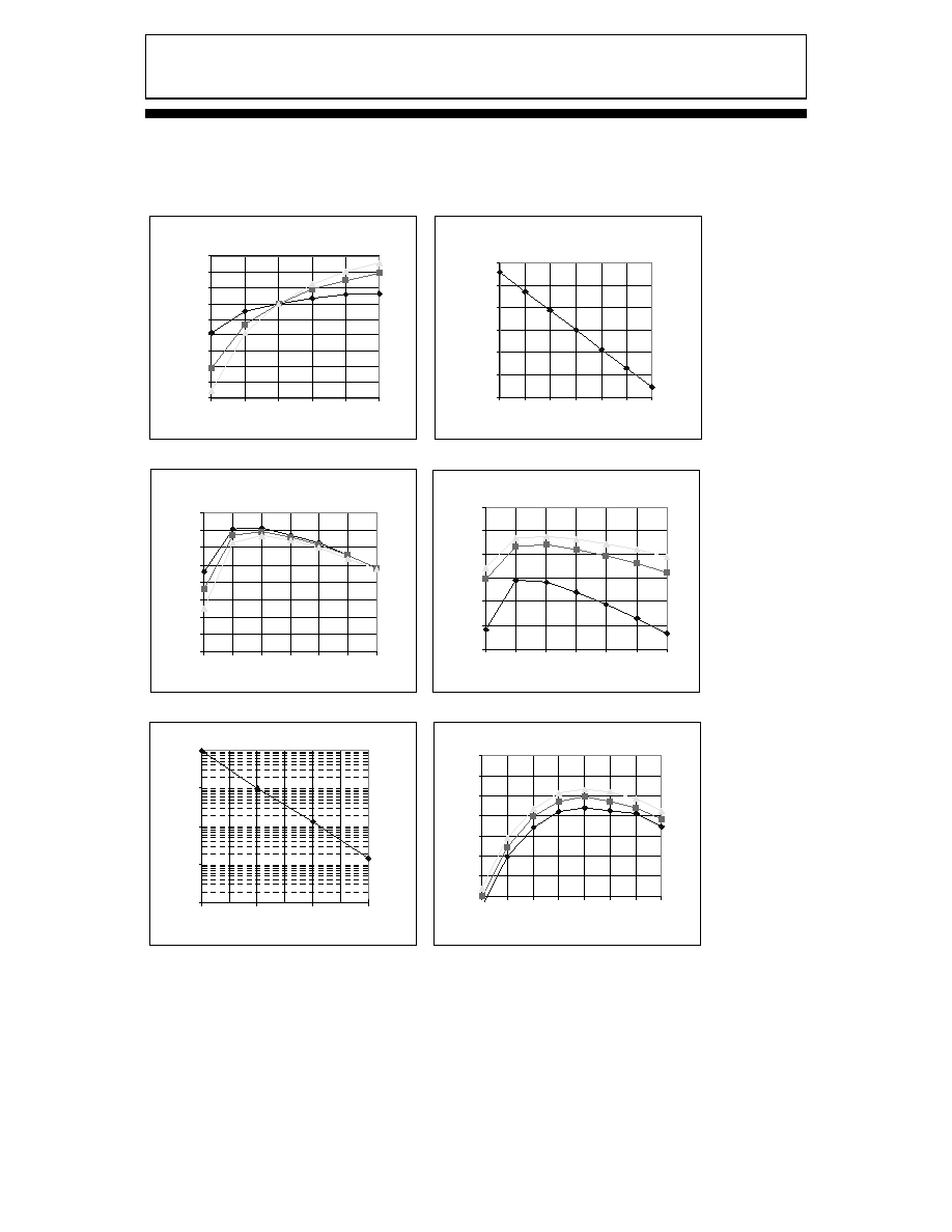
Typical Performance Curves
Line Regulation vs. Cs lope (Iout=3A)
0.0%
0.1%
0.2%
0.3%
0.4%
0.5%
0.6%
0.7%
0.8%
50
75
100
125
150
175
Cslope(pF)
C
h
a
n
g
e
V
o
u
t
(
+
/-
)
Vout=3.5V
Vout=2.5V
Vout=1.0V
Vdd=Vin=5.0V +/-10%
Ta=25C
Line Regulation (C
Slope
=100pF)
3.46
3.47
3.48
3.49
3.5
3.51
3.52
3.53
3.54
4.5V
5.0V
5.5V
Vin (V)
V
out
(
V
)
I
out
=.5A
I
out
=6A
I
out
=3A
Ta=25C
Line Regulation vs. Cs lope
Vin=Vdd=5.0V +/- 10%
0.0%
0.1%
0.2%
0.3%
0.4%
0.5%
0.6%
0.7%
0.8%
50
75
100
125
150
175
Cs lope (pF)
Cha
nge
V
out
(
+
/
-
)
Ta=25C
I
out
=6A
I
out
=.5A
Load Re gulation, (C
slope
=100pF)
3.46
3.47
3.48
3.49
3.5
3.51
3.52
3.53
3.54
0.5
3
6
Iout (A)
Vo
u
t
(
V
)
Vin=5.5 V
Vin=4.5 V
Vin=5.0 V
Ta=25C
Load Re gulation vs . Cslope
Iout =3A, +3A, -2.5A
0.0%
0.1%
0.2%
0.3%
0.4%
0.5%
0.6%
0.7%
0.8%
50
75
100
125
150
175
Cs lope (pF)
C
h
a
n
ge
V
o
ut
(
+
/
-
)
Ta=25C
Vin=5.5V
Vin=4.5V
Vin=5.0V
Load Re gulation vs . Cslope (Vin=5.0V)
Iout 3A +3A,-2.5A
0.0%
0.1%
0.2%
0.3%
0.4%
0.5%
0.6%
50
75
100
125
150
175
Cslope(pF)
Cha
nge
V
out
(
+
/
-
)
Vout=3.5V
Vout=1.0V
Ta=25C
Vout=2.5V
EL7556C
Adjustable CPU Power Supply Unit
10
Typical Performance Curves
Vout vs. Cs lope
(Vin=5.0V, Iload=.5A)
-3.0%
-2.5%
-2.0%
-1.5%
-1.0%
-0.5%
0.0%
0.5%
1.0%
1.5%
50
75
100
125
150
175
Cslope (pF)
Cha
nge
V
out
Vout=1.0V
Vout=3.5V
Vout=2.5V
Ta=25C, C
OSC
=220pF
Efficiency vs . Iload (Vout=3.5V)
VDD=VIN=5.5V +/- 10%)
80%
82%
84%
86%
88%
90%
92%
94%
96%
0.5
1.5
2.5
3.5
4.5
5.5
6.5
Iout (A)
E
f
fi
ci
e
n
cy
Ta=25C
Vdd=5.5V
Vdd=5.0V
Vdd=4.5V
Efficiency vs . Iload (VDD=5.0V)
70%
75%
80%
85%
90%
95%
100%
0.5
1.5
2.5
3.5
4.5
5.5
6.5
Iout (A)
E
f
fi
ci
e
n
cy
Vout=3.5V
Vout=2.5V
Vout=1.0V
Vout Variation vs. Program m e d Output
Voltage (Vide al=(1+R3/R4))
-1.5%
-1.0%
-0.5%
0.0%
0.5%
1.0%
1.5%
1
1.5
2
2.5
3
3.5
4
Videal(V)
D
e
v
i
a
t
io
n
in
V
o
u
t
Ta=25C
Cslope=100pF
Cosc=220pF
Loop Gain Induced Error
Fos c vs . Cos c
1
10
100
1000
10000
10
100
1000
10000
Cos c(pF)
Fos
c
(
k
H
z)
Ta=25C
Fosc vs. Temp
450
460
470
480
490
500
510
520
0
20
40
60
80
100 120 140
Tem p (
o
C)
fo
sc
(
k
H
z
)
Ta=25C
Vdd=5.0V
Vdd=5.5V
Vdd=4.5V

EL7556C
Adjustable CPU Power Supply Unit
11
Typical Performance Curves
I(VIN) vs. fosc
0
2
4
6
8
10
12
14
16
100
200
300
400
500
600
700
800
900 1000
fos c (k Hz)
IV
IN
(
m
A
)
VDD=5.5V
VDD=4.5V
VDD=5.0V
Ta=25C
OUTEN=VDD
Discontinuous Mode
Continuous Mode
I(VDD)+I(VIN) vs . fos c
0
10
20
30
40
50
60
100
200
300
400
500
600
700
800
900 1000
fosc (kHz)
Iq
(
m
A
)
VDD=5.5V
VDD=4.5V
VDD=5.0V
Ta=25C
OUTEN=VDD
Discontinuous Mode
Continuous Mode
I(VDD) vs . fos c
0
5
10
15
20
25
30
35
40
45
50
100
200
300
400
500
600
700
800
900 1000
fosc(k Hz)
I
dd (
m
A)
VDD=5.5V
VDD=4.5V
VDD=5.0
Ta=25C
OUTEN=VDD
IDD+IVIN vs . fos c
1.0
1.5
2.0
10
100
1000
fos c (k Hz)
Id
d
+
I
v
in
(
m
A
)
Ta=25C
OUTEN=0V
VDD=5.5V
VDD=4.5
VDD=5.0V
Pow er On Res et
0
10
20
30
40
2.5
3
3.5
4
4.5
5
VDD(V)
Iq
(
m
A
)
Ta=25C
OUTEN=VDD
fosc=500k
Minimum Output Voltage vs. fosc
0.7
0.9
1.1
1.3
1.5
1.7
1.9
2.1
2.3
100 200 300 400 500 600 700 800 900 1000
fosc (kHz)
Vo
u
t
(
V
)
Tj=120C
VDD=5.5V
VDD=4.5V
VDD=5.0V

EL7556C
Adjustable CPU Power Supply Unit
12
Typical PerformanceCurves
The ta JM vs. Cu Are a
25
27
29
31
33
35
37
39
41
0.00
1.00
2.00
3.00
4.00
5.00
6.00
Bare Cu Ar e a (in^2)
T
h
e
t
a JM
(
o
C/
W
)
Board w ith no Components
Board w ith inductor
Ma x im um Iloa d vs. Te m pe ra ture
EL7556 De m o Boa rd (31
o
C/W )
4
4.5
5
5.5
6
6.5
7
7.5
8
25
30 35
40
45 50
55
60 65
70
Ta (
o
C)
I
l
oa
d (
A
)
100 LFM
Still Air
OUTEN connected to OT
R
DSON
vs. Te m p
20
22
24
26
28
30
32
34
36
38
0
25
50
75
100
125
Te m p (
o
C)
R
DS
O
N
(m
)
Top Trace: V(LX)
Bottom Trace: VOUT, ILOAD=6A VOUT, IL= .5A to 6A Load Step

EL7556C
Adjustable CPU Power Supply Unit
13
Block Diagram
C
O
SC
,
Pi
n 4
CSL
O
PE
,
Pi
n 3
CR
EF,
pi
n 27
PW
RG
D,
Pi
n
16
L
X
,
Pi
n 20-23
V
H
I,
P
i
n
24
+
-
1.17V Ref
V
S
S
P
,
Pi
n 9
-
12,
18-1
9
+
-
V
D
D
and V
I
N
,
P
i
n 5,
6,
8
2-1 MUX
+
-
+
-
LE
B Tdel
ay
R
S
Q
Q
FF
+
-
Zero
C
r
oss
D
e
tect
VD
D
Rs
s
Cs
s
VD
D
+
_
+
_
VD
D
S
R
R
S
VDD
4V
UV
LO
Ov
e
r
T
e
m
p
Se
nsor
O
T
,
P
i
n 15
V2
X
C
2
V
,
Pi
n 26
C
P
,
Pi
n 27
Vs
s
,
Pi
n
2
5
PW
M
Cur
r
e
n
t
Li
m
i
t
Cu
rrent
Se
nse
VCC
2
DE
T,
P
i
n
1
3
VD
D
FB1
,
Pi
n
1
FB2
,
Pi
n2
8
O
U
T
E
N
,
p
i
n
14
+
-
VD
D