 | –≠–ª–µ–∫—Ç—Ä–æ–Ω–Ω—ã–π –∫–æ–º–ø–æ–Ω–µ–Ω—Ç: EL7558BCM | –°–∫–∞—á–∞—Ç—å:  PDF PDF  ZIP ZIP |
Note: All information contained in this data sheet has been carefully checked and is believed to be accurate as of the date of publication; however, this data sheet cannot be a "controlled document". Current revisions, if any, to these
specifications are maintained at the factory and are available upon your request. We recommend checking the revision level before finalization of your design documentation.
© 2001 Elantec Semiconductor, Inc.
E
L
7
5
5
8
B
C
General Description
The EL7558BC is an adjustable synchronous DC:DC switching regu-
lator optimized for a 5V input and 1.0V-3.8V output. By combining
integrated NMOS power FETS with a HSOP package the EL7558BC
can supply up to 8A continuous output current without the use of
external power devices or externally attached heat sinks, thereby min-
imizing design effort and overall system cost.
On-chip resistorless current sensing is used to achieve stable, highly
efficient, current-mode control. The EL7558BC also incorporates the
VCC2DET function to directly interface with the Intel P54 and P55
microprocessors. Depending on the state of VCC2DET, the output
voltage is internally preset to 3.50V or a user-adjustable voltage using
two external resistors. In both internal and external feedback modes
the active-high PWRGD output indicates when the regulator output is
within ±10% of the programmed voltage. An on-board sensor moni-
tors die temperature (OT) for over-temperature conditions and can be
connected directly to OUTEN to provide automatic thermal shutdown.
Adjustable oscillator frequency and slope compensation allow added
flexibility in overall system design.
The EL7558BC is available in the 28-pin HSOP package and is speci-
fied for operation over the -40∞C to +85∞C temperature range.
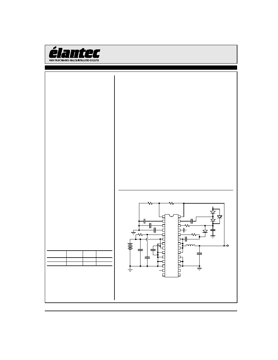
Connection Diagram
Manufactured under U.S. Patents No. 5,723,974 and No. 5,793,126
1
2
3
4
16
15
14
13
5
6
7
12
11
9
8
10
20
19
18
17
24
23
22
21
EL7558BC
28
27
26
25
FB1
VSS
VHI
LX
LX
LX
LX
VSSP
VSSP
VSSP
VSSP
VIN
VIN
VDD
COSC
CSLOPE
CREF
TEST
VSSP
VSSP
VCC2DET
OUTEN
OT
VSSP
CP
FB2
C2V
C4
C8
C7
D1
C10
L1
C11
R1
C 6
R5
R6
C3
0.22µF
20
2.5µH
1mF
220pF
330pF
0.1µF
1µF
39.2
0.1µF
5.1
C9
660µF
V
OUT
D2
D3
C 5
1µF
R4
R3
100
150
Connect to VSSP for
external feedback
PWRGD
V
IN
V
IN
C3, C4, C5, C6, C7 C8 - ceramic
C5, C11 - ceramic or tantalum
C9 - Sprague 293D337X96R3 2X330µF
C10 - Sprague 293D337X96R3 3X330µF
L1 - Pulse Engineering, PE-53681
D1 - D4: BAT54S fast diode
1µF
C12
D4*
(Optional)
D4 Required for EL7558ACM only
C12 = 1µF
Features
∑ EL7558C/EL7558AC pin-
compatible
∑ Improved temperature and voltage
ranges
∑ 8A continuous load current
∑ Precision internal 1% reference
∑ 1.0V to 3.8V output voltage
∑ Internal power MOSFETs
∑ >90% efficiency
∑ Synchronous switching
∑ Adjustable slope compensation
∑ Over-temperature indicator
∑ Pulse-by-pulse current limiting
∑ Operates up to 1MHz
∑ 1.5% typical output accuracy
∑ Adjustable oscillator with sync
∑ Remote enable/disable
∑ Intel P54- and P55-compatible
∑ VCC2DET interface
∑ Internal soft-start
Applications
∑ PC motherboards
∑ Local high power CPU supplies
∑ 5V to 1.0V DC:DC conversion
∑ Portable electronics/instruments
∑ P54 and P55 regulators
∑ GTL+ Bus power supply
Ordering Information
Part No
Package
Tape &
Reel
Outline #
EL7558BCM
28-Pin HSOP
-
MDP0042
EL7558BCM-T13
28-Pin HSOP
13"
MDP0042
EL7558BC
Integrated Adjustable 8 Amp Synchronous Switcher
A
p
r
i
l
2
7
,
2
0
0
1
2
EL7558BC
Integrated Adjustable 8 Amp Synchronous Switcher
E
L
7
5
5
8
B
C
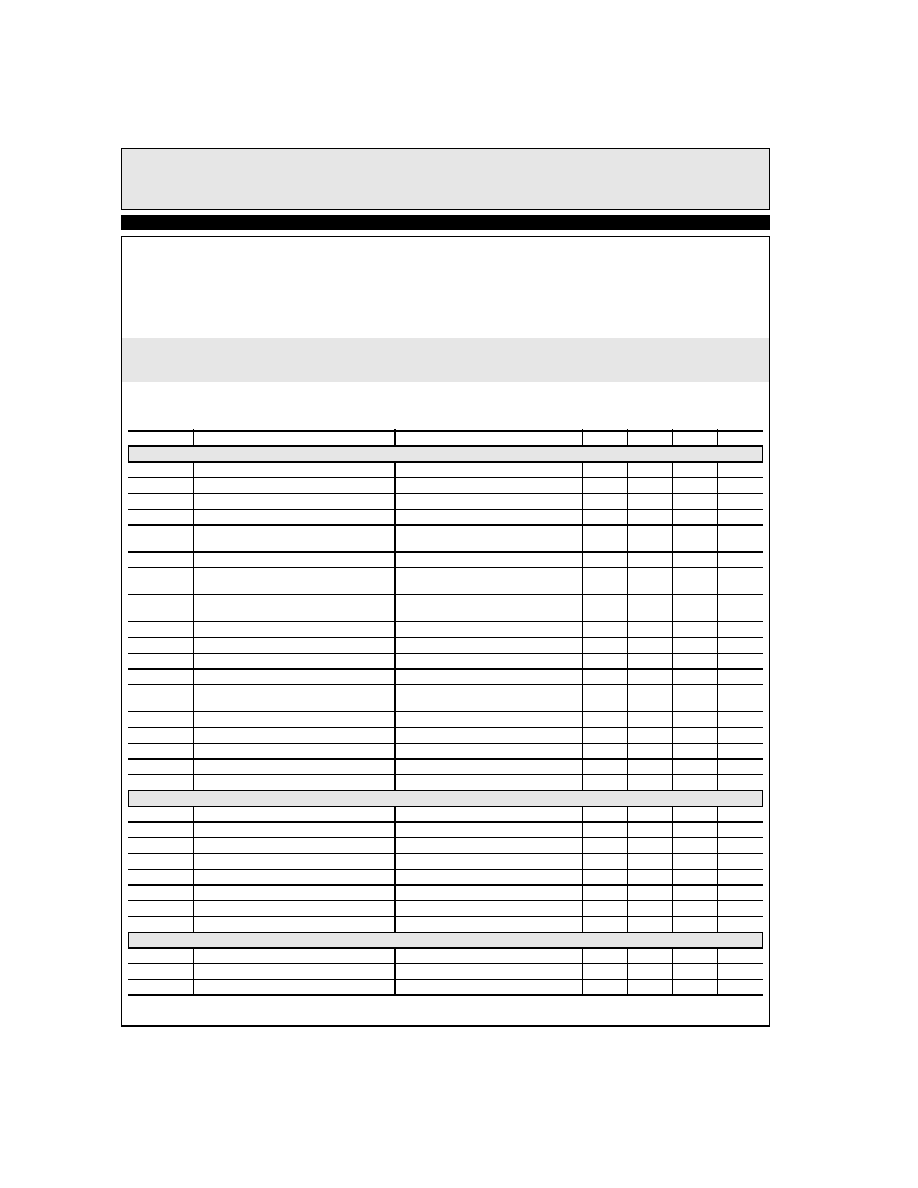
Absolute Maximum Ratings
(T
A
= 25∞C)
Storage Temperature Range
-65∞C to +150∞C
Supply (V
IN
)
6V
Ambient Operating Temperature
-40∞C to +85∞C
Output Pins
-0.3V below GND, +0.3V above VDD
Operating Junction Temperature
135∞C
Peak Output Current
9A
Electrical Characteristics
V
DD
= V
IN
= 5V, C
OSC
= 1nF, C
SLOPE
= 470pF, T
A
= 25∞C unless otherwise specified.
Parameter
Description
Conditions
Min
Typ
Max
Unit
General
I
DD
V
DD
Supply Current
OUTEN = 4V, F
OSC
= 120kHz
11
25
mA
I
DDOFF
V
DD
Standby Current
OUTEN = 0
0.1
mA
I
VIN
V
IN
No Load Current
OUTEN = 0
3
5
mA
V
OUT1
Output Initial Accuracy
VCC2DET = 4V, IL = 3A (See Fig. 1)
3.450
3.500
3.550
V
V
OUT2
Output Initial Accuracy
VCC2DET = 0V, IL = 3A R3 = 150
, R4 =
100
(See Fig. 1)
2.450
2.500
2.550
V
V
OUTLINE
Output line Regulation
VDD = 5V, ±10%
-1
1
%
V
OUTLOAD
Output Load Regulation
0A<I
LOAD
<6A, Relative to IL = 3A. Continu-
ous Mode of Operation (See Fig.1)
-1
1
%
R
SHORT
Short Circuit Load Resistance
IL = 6A Prior to Continuous Application of
R
SHORT
. OUTEN Connected to OT.
100
m
I
I MAX
Current Limit
9
A
V
OUTTC
Output Tempco
-40∞C<T
A
<85∞C
±1
%
T
OT
Over Temperature Threshold
135
∞C
T
HYS
Over Temperature Hysteresis
40
∞C
V
PWRGD
Power Good Threshold Relative to Programmed
Output Voltage
VCC2SEL = 4V, V
OUT
= 3.50V
±6
±10
±14
%
V
DDOFF
Minimum VDD for Shutdown
3.15
V
V
DDON
Maximum VDD for Startup
4.15
V
V
HYS
Input Hysteresis
V
HYS
= V
DDON
-V
DDOFF
0.5
V
M
SS
Soft start slope
7
V/ns
DMAX
Maximum duty cycle
96
%
Controller - Inputs
I
PUP
VCC2DET, OUTEN Pull Up Current
VCC2DET, OUTEN = 0
10
14
18
µA
I
CSLOPE
Cslope Charging Current
23
28.5
34
µA
I
FB1
FB1 Input Pull Up Current
2
µA
R
OT
Over Temperature Pull Up Resistance
OT = 0V
30
40
50
k
V
IH
VCC2DET, OUTEN Input High
4
V
V
IL
VCC2DET, OUTEN Input Low
.8
V
V
OH
PWGD
Powergood Drive High
ILoad = 1mA
3.5
V
V
OL PWGD
Powergood Drive Low
ILoad = -1mA
1.0
V
Controller - Reference
V
REF
Reference Accuracy
I
REF
= 0
1.247
1.260
1.273
V
V
REFTC
Reference Voltage Tempco
50
ppm/∫C
V
REFLOAD
Reference Load Regulation
0<I
LOAD
<100µA
0.5
0.5
%/∫C
Important Note:
All parameters having Min/Max specifications are guaranteed. Typ values are for information purposes only. Unless otherwise noted, all tests are at the
specified temperature and are pulsed tests, therefore: T
J
= T
C
= T
A
.

3
EL7558BC
Integrated Adjustable 8 Amp Synchronous Switcher
E
L
7
5
5
8
B
C
Controller - Doubler
V
C2V
Voltage Doubler Output
V
DD
= 5V, I
LOAD
= 10mA
7.5
8.1
8.7
V
Controller - Oscillator
F
RAMP
Oscillator Ramp Amplitude
1.2
V
I
OSC CHG
Oscillator Charge Current
0.2V<V
OSC
<1.4V
150
µA
I
OSC DIS
Oscillator Discharge Current
0.2V<V
OSC
<1.4V
5
mA
F
OSC
Oscillator initial accuracy
100
120
140
kHz
t
sync
Minimum oscillator sync width
50
ns
Power - FET
I
LEAK
LX Output Leakage to VSS
LX = 0V
100
µA
R
DSON
Composite FET Resistance
18
30
m
R
DSONTC
R
DSON
Tempco
0.1
m
/∫C
tbrm
FET break before make delay
10
ns
tLEB
High side FET minimum on time (LEB)
140
ns
Electrical Characteristics
V
DD
= V
IN
= 5V, C
OSC
= 1nF, C
SLOPE
= 470pF, T
A
= 25∞C unless otherwise specified.
Parameter
Description
Conditions
Min
Typ
Max
Unit
4
EL7558BC
Integrated Adjustable 8 Amp Synchronous Switcher
E
L
7
5
5
8
B
C
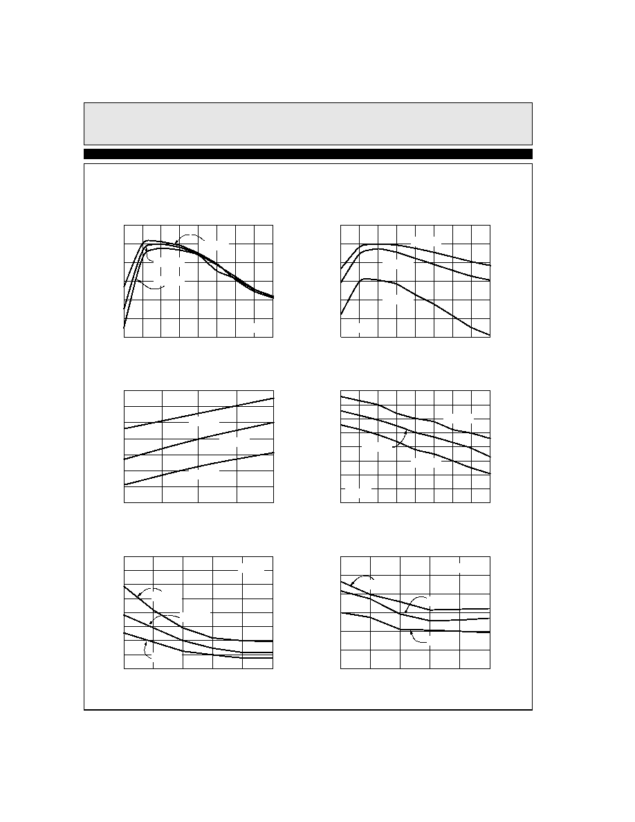
Typical Performance Curves
50
75
0.4
0.5
0.8
C
SLOPE
(pF)
V
O
U
T
(
±
)
(
%
)
0.6
0.7
100
125
150
175
Line Regulation vs C
SLOPE
(I
OUT
=3A)
V
DD
=V
IN
=5.0V ±10%
0.0
0.1
0.2
0.3
Load Regulation (C
SLOPE
=150pF)
3.47
3.54
3.53
3.52
3.51
3.50
3.49
3.48
3.46
V
O
U
T
(
V
)
I
OUT
(A)
0.5
3
8
6
1
2
4
5
7
Line Regulation (C
SLOPE
=150pF)
3.54
3.53
3.52
3.51
3.50
3.49
3.48
3.47
V
O
U
T
(
V
)
V
IN
(V)
4.5
5.0
5.5
93
95
97
I
OUT
(A)
E
f
f
i
c
i
e
n
c
y
(
%
)
8.0
Efficiency vs I
LOAD
(V
OUT
=3.5V)
85
87
89
91
0.5
2.5
3.5
5.5
6.5
7.5
1.5
4.5
90
95
100
I
OUT
(A)
E
f
f
i
c
i
e
n
c
y
(
%
)
8.0
Efficiency vs I
LOAD
(V
DD
=5.0 V)
70
75
80
85
0.5
2.5
3.5
5.5
6.5
7.5
1.5
4.5
50
75
0.4
0.5
0.6
C
SLOPE
(pF)
V
O
U
T
(
±
)
(
%
)
100
125
150
175
Load Regulation vs C
SLOPE
(V
IN
=5.0V)
I
OUT
=0.5 to 6A
0.0
0.1
0.2
0.3
V
DD
=4.5V
V
DD
=5V
V
DD
=5.5V
T
A
=25∞C
V
OUT
=3.5V
T
A
=25∞C
V
OUT
=2.5V
V
OUT
=1V
I
OUT
=0.5A
T
A
=25∞C
I
OUT
=4A
I
OUT
=8A
V
IN
=5.5V
T
A
=25∞C
V
IN
=4.5V
V
IN
=5V
V
OUT
=3.5V
T
A
=25∞C
V
OUT
=2.5V
V
OUT
=1V
V
OUT
=3.5V
T
A
=25∞C
V
OUT
=2.5V
V
OUT
=1V
5
EL7558BC
Integrated Adjustable 8 Amp Synchronous Switcher
E
L
7
5
5
8
B
C
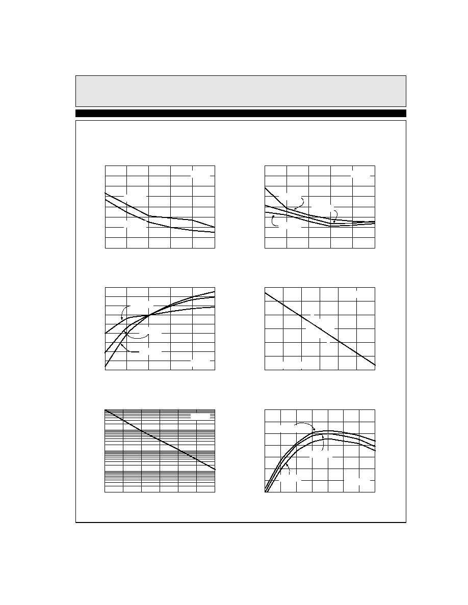
Typical Performance Curves
50
75
-0.5
0.0
1.5
C
SLOPE
(pF)
V
O
U
T
(
±
)
(
%
)
0.5
1.0
100
125
150
175
V
OUT
vs C
SLOPE
(V
IN
=5.0V, I
LOAD
=.5A)
-3.0
-2.0
-1.5
-1.0
-2.5
1.0
1.5
0.5
1.0
1.5
V
IDEAL
(V)
D
e
v
i
a
t
i
o
n
i
n
V
O
U
T
(
%
)
2.0
2.5
3.0
4.0
V
OUT
Variation vs Programmed Output
Voltage [V
IDEAL
=(1+R3/R4)]
-1.5
-1.0
-0.5
0.0
3.5
50
75
0.4
0.5
0.8
C
SLOPE
(pF)
V
O
U
T
(
±
)
(
%
)
0.6
0.7
100
125
150
175
Line Regulation vs C
SLOPE
V
IN
=V
DD
=5.0V ±10%
0.0
0.1
0.2
0.3
50
75
0.4
0.5
0.8
C
SLOPE
(pF)
V
O
U
T
(
±
)
(
%
)
0.6
0.7
100
125
150
175
Load Regulation vs C
SLOPE
I
OUT
=0.5 to 6A
0.0
0.1
0.2
0.3
0
20
490
510
520
Temperature (∞C)
F
O
S
C
(
k
H
z
)
40
60
80
140
450
460
470
480
F
OSC
vs Temperature
100
500
120
F
O
S
C
(
k
H
z
)
10000
10
C
OSC
(pF)
F
OSC
vs C
OSC
1000
100
10
1
100000
100
1000
T
A
=25∞C
I
OUT
=6A
I
OUT
=0.5A
T
A
=25∞C
V
IN
=4.5A
V
IN
=5A
V
IN
=5.5A
T
A
=25∞C
V
OUT
=1V
V
OUT
=2.5V
V
OUT
=3.5V
T
A
=25∞C
C
SLO
PE
=100
pF
C
OSC
=220
pF
Loop Gain Induced Error
T
A
=25∞C
V
DD
=4.5V
V
DD
=5.5V
V
DD
=5V
C
OSC
=220pF