 | –≠–ª–µ–∫—Ç—Ä–æ–Ω–Ω—ã–π –∫–æ–º–ø–æ–Ω–µ–Ω—Ç: ELH0032 | –°–∫–∞—á–∞—Ç—å:  PDF PDF  ZIP ZIP |

ELH0032G8838001301ZX
July
1991
Rev
F
ELH0032G 883 8001301ZX
Fast Operational Amplifier
Note All information contained in this data sheet has been carefully checked and is believed to be accurate as of the date of publication however this data sheet cannot be a ``controlled document'' Current revisions if any to these
specifications are maintained at the factory and are available upon your request We recommend checking the revision level before finalization of your design documentation
CMS
0032DS
1986 Elantec Inc
Features
500 V ms slew rate
70 MHz bandwidth
10
12
X input impedance
5 mV max input offset voltage
FET input
Offset nulls with single pot
No compensation required for
gains above 50
Peak output current to 100 mA
MIL-STD-883 devices 100%
manufactured in U S A
Ordering Information
Part No
Temp Range Pkg Outline
ELH0032G 883B b55 C to a125 C TO-8 MDP0002
8001301ZX is the SMD version of this device
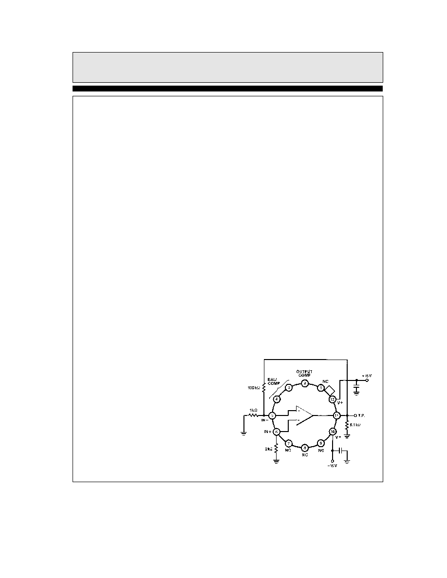
Connection Diagram
0032 ≠ 1
Top View
Case is electrically isolated
Manufactured under U S Patent No 4 746 877
General Description
The ELH0032 is a high slew rate high input impedance differ-
ential operational amplifier suitable for diverse application in
fast signal handling The high allowable differential input volt-
age ease of output clamping and high output drive capability
make the ELH0032 particularly suitable for comparator appli-
cations It may be used in applications normally reserved for
video amplifiers allowing the use of operational gain setting and
frequency response shaping into the megahertz region
The ELH0032's wide bandwidth high input impedance and
high output drive capability make it an ideal choice for applica-
tions such as summing amplifiers in high-speed D to A's buff-
ers in data acquisition systems and sample and hold circuits
Additional applications include high-speed integrators and vid-
eo amplifiers The ELH0032 is guaranteed over the temperature
range
b
55 C to
a
125 C
Elantec facilities comply with MIL-I-45208A and other applica-
ble quality specifications Elantec's Military devices are 100%
fabricated and assembled in our rigidly controlled ultra-clean
facilities in Milpitas California For additional information on
Elantec's Quality and Reliability Assurance policy and proce-
dures request brochure QRA-1
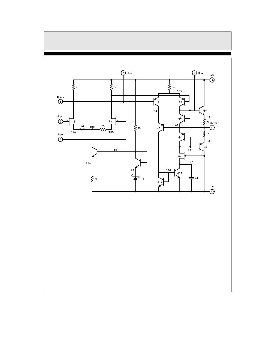
Simplified Schematic
0032 ≠ 2
ELH0032G 883 8001301ZX
Fast Operational Amplifier
Absolute Maximum Ratings
V
S
Supply Voltage
g
18V
V
IN
Input Voltage
g
15 V
S
Differential Input Voltage
g
30V or
g
2 V
S
P
D
Power Dissipation (Note 1)
T
A
e
25 C
1 5W derate 100 C W to
a
125 C
T
C
e
25 C
2 2W derate 70 C W to
a
125 C
T
A
Operating Temperature Range
ELH0032
b
55 C to
a
125 C
T
J
Operating Junction Temperature
175 C
T
ST
Storage Temperature
b
65 C to
a
150 C
Lead Temperature
(Soldering 10 seconds)
300 C
Important Note
All parameters having Min Max specifications are guaranteed The Test Level column indicates the specific device testing actually
performed during production and Quality inspection Elantec performs most electrical tests using modern high-speed automatic test
equipment specifically the LTX77 Series system Unless otherwise noted all tests are pulsed tests therefore T
J
e
T
C
e
T
A
Test Level
Test Procedure
I
100% production tested and QA sample tested per QA test plan QCX0002
II
100% production tested at T
A
e
25 C and QA sample tested at T
A
e
25 C
T
MAX
and T
MIN
per QA test plan QCX0002
III
QA sample tested per QA test plan QCX0002
IV
Parameter is guaranteed (but not tested) by Design and Characterization Data
V
Parameter is typical value at T
A
e
25 C for information purposes only
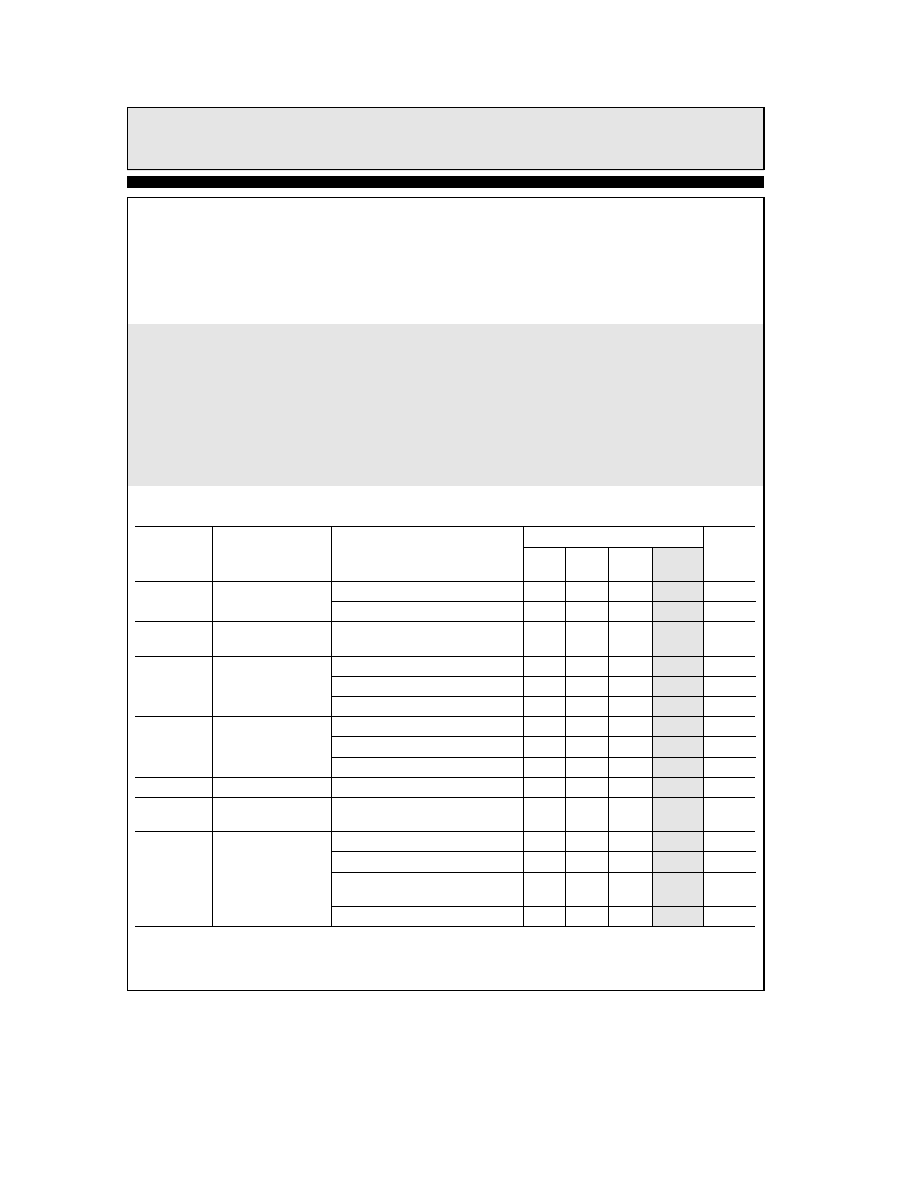
DC Electrical Characteristics
V
S
e
g
15V T
MIN
s
T
A
s
T
MAX
V
IN
e
0V
Parameter
Description
Test Conditions
ELH0032
Units
Min
Typ
Max
Test
Level
V
OS
Input Offset Voltage
T
J
e
25 C (Note 2)
2
5
I
mV
10
I
mV
DV
OS
DT
Average Offset
25
150
I
mV C
Voltage Drift
I
OS
Input Offset Current
T
J
e
25 C (Note 2)
25
I
pA
T
A
e
25 C (Note 3)
250
IV
pA
T
J
e
Max
25
I
nA
I
B
Input Bias Current
T
J
e
25 C (Note 2)
100
I
pA
T
A
e
25 C (Note 3)
1
IV
nA
T
J
e
T
MAX
50
I
nA
V
INCM
Input Voltage Range
g
10
g
12
I
V
CMRR
Common-Mode
V
IN
e
g
10V
50
60
I
dB
Rejection Ratio
A
VOL
Open-Loop
V
O
e
g
10V R
L
e
1 k
X T
J
e
25 C
48
60
I
dB
Voltage Gain
V
O
e
g
10V R
L
e
1 k
X
45
I
dB
V
O
e
g
10V f
e
1 kHz
60
70
I
dB
R
L
e
1 k
X T
J
e
25 C
V
O
e
g
10V f
e
1 kHz R
L
e
1 k
X
57
I
dB
2
TD
is
07in
TD
is
37in
ELH0032G 883 8001301ZX
Fast Operational Amplifier
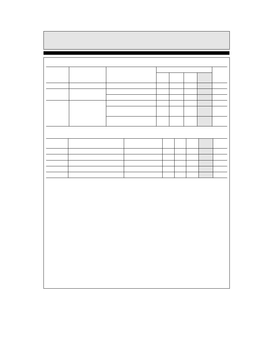
DC Electrical Characteristics
V
S
e
g
15V T
MIN
s
T
A
s
T
MAX
V
IN
e
0V
Contd
Parameter
Description
Test Conditions
ELH0032
Units
Min
Typ
Max
Test
Level
V
O
Output Voltage Swing
R
L
e
1 k
X
g
10
g
13 5
I
V
I
S
Power Supply Current
T
J
e
25 C I
O
e
0 mA
21
23
I
mA
T
A
e
25 C I
O
e
0 mA (Note 3)
18
20
IV
mA
PSRR
Power Supply
g
5V
s
V
S
s
15V
50
60
I
dB
Rejection Ratio
a
5V
s
V
S
(
a
)
s
a
20V
50
I
dB
V
S
(
b
)
e b
15V
b
5V
t
V
S
(
b
)
t
b
20V
50
I
dB
V
S
(
a
)
e a
15V
AC Electrical Characteristics
V
S
e
g
15V R
L
e
1 k
X T
J
e
25 C
Parameter
Description
Test Conditions
Min
Typ
Max
Test
Units
Level
SR
Slew Rate
A
V
e a
1
DV
IN
e
20V
350
500
I
V
ms
t
S
Settling Time to 1% of Final Value
A
V
e b
1
DV
IN
e
20V
100
500
IV
ns
t
S
Settling Time to 0 1% of Final Value
A
V
e b
1
DV
IN
e
20V
300
V
ns
t
R
Small Signal Rise Time
A
V
e a
1
DV
IN
e
1V
8
20
I
ns
t
D
Small Signal Delay Time
A
V
e a
1
DV
IN
e
1V
10
25
I
ns
Note 1 In order to limit maximum junction temperature to
a
175 C it may be necessary to operate with V
S
k g
15V when T
A
or T
C
exceeds specific values depending on the P
D
within the device package Total P
D
is the sum of quiescent and load-related
dissipation
Note 2 Specification is at 25 C junction temperature due to requirements of high-speed automatic testing Actual values at operating
temperature will exceed the value at T
J
e
25 C When supply voltage are
g
15V no-load operating junction temperature
may rise 40 C ≠ 60 C above ambient and more under load conditions Accordingly V
OS
may change one to several mV and I
B
and I
OS
will change significantly during warm-up Refer to I
B
and I
OS
vs temperature graph for expected values
Note 3 Measured in still air 7 minutes after application of power
3
TD
is
19in
TD
is
13in
ELH0032G 883 8001301ZX
Fast Operational Amplifier
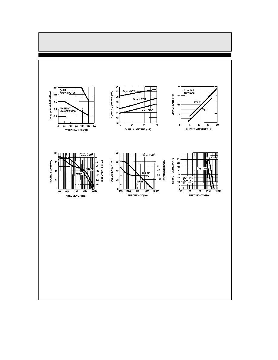
Typical Performance Curves
Dissipation
Maximum Power
Supply Voltage
Supply Current vs
vs Supply Voltage
and Output Voltage
Input Voltage Range
(Uncompensated)
Bode Plot
Gain Compensation)
Bode Plot (Unity
Frequency Response
Large Signal
0032 ≠ 3
4
ELH0032G 883 8001301ZX
Fast Operational Amplifier
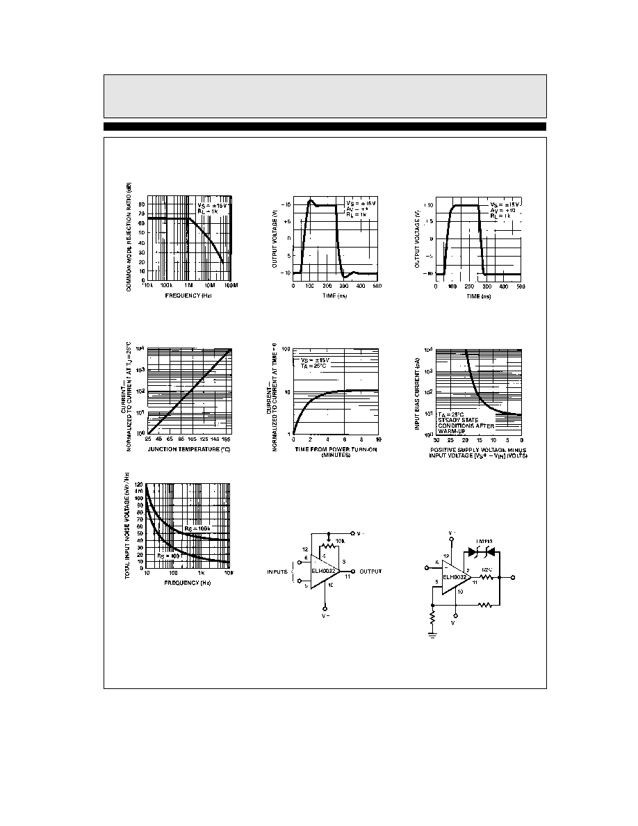
Typical Performance Curves
Contd
vs Frequency
Rejection Ratio
Common Mode
Pulse Response
Large Signal
Pulse Response
Large Signal
vs Junction Temperature
and Offset Current
Normalized Input Bias
Current During Warm-Up
Normalized Input Bias
vs Input Voltage
Input Bias Current
0032 ≠ 4
Total Input Noise Voltage
vs Frequency
0032 ≠ 5
Noise voltage includes contri-
bution from source resistance
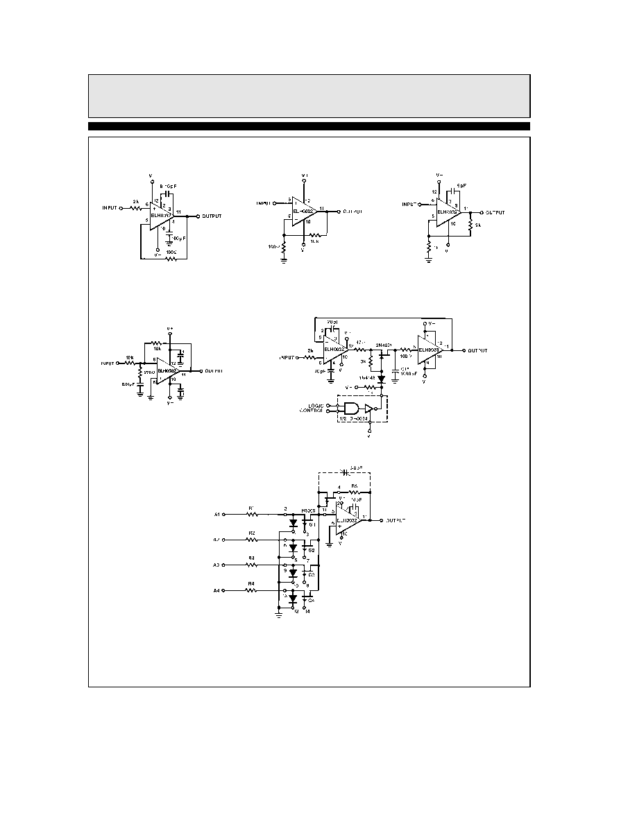
Auxiliary Circuits
Offset Null
0032 ≠ 6
Output Short Circuit Protection
0032 ≠ 7
5
ELH0032G 883 8001301ZX
Fast Operational Amplifier
Typical Applications
Unity Gain Amplifier
0032 ≠ 8
TYP BW
3 dB
e
45 MHz
100X Buffer Amplifier
0032 ≠ 9
TYP BW
3 dB
e
10 MHz
10X Buffer Amplifier
0032 ≠ 10
TYP BW
3 dB
e
5 MHz
Non-Compensated Unity
Gain Inverter
0032 ≠ 11
TYP BW
3 dB
e
70 MHz
High-Speed Sample and Hold
Low leakage for minimum drift
0032 ≠ 12
High-Speed Current Mode MUX
0032 ≠ 13
6
ELH0032G 883 8001301ZX
Fast Operational Amplifier
Applications Information
Power Supply Decoupling
The ELH0032 like most high-speed circuits is
sensitive to layout and stray capacitance Power
supplies should be bypassed as near to pins 10
and 12 as possible with low inductance capacitors
such as 0 01
mF disc ceramics Compensation
components should also be located close to the
appropriate pins to minimize stray reactances
Input Current
Because the input devices are FETs the input
bias current may be expected to double for each
11 C junction temperature rise This characteris-
tic is plotted in the typical performance charac-
teristics graphs The device will self-heat due to
internal power dissipation after application of
power thus raising the FET junction tempera-
ture 40 C ≠ 60 C above the free-air ambient tem-
perature when supplies are
g
15V The device
temperature will stabilize within 5 ≠ 10 minutes
after application of power and the input bias cur-
rents measured at the time will be indicative of
normal operating currents An additional rise will
occur as power is delivered to a load due to addi-
tional internal power dissipation
There is an additional effect on input bias current
as the input voltage is changed The effect com-
mon to all FETs is an avalance-like increase in
gate current as the FET gate-to-drain voltage is
increased above a critical value depending on
FET geometry and doping levels This effect will
be noted as the input voltage of the ELH0032 is
taken below ground potential when the supplies
are
g
15V All of the effects described here may
be minimized by operating the device with V
S
s
g
15V
These effects are indicated in the typical per-
formance curves
Input Capacitance
The input capacitance to the ELH0032 is typical-
ly 5 pF and thus may form a significant time
constant with high value resistors For optimum
performance the input capacitance to the invert-
ing input should be compensated by a small ca-
pacitor across the feedback resistor The value is
strongly dependent on layout and closed loop
gain but will typically be in the neighborhood of
several picofarads
In the non-inverting configuration it may be ad-
vantageous to bootstrap the case and or a guard
conductor to the inverting input
This serves
both to divert leakage currents away from the
non-inverting input and to reduce the effective
input capacitance A unity gain follower so treat-
ed will have an input capacitance under a 1 pF
Heatsinking
While the ELH0032 is specified for operation
without any explicit heatsink internal power dis-
sipation does cause a significant temperature rise
Improved bias current performance can thus be
obtained by limiting this temperature rise with a
small heat sink such as the Thermalloy No 2241
or equivalent The case of the device has no inter-
nal connection so it may be electrically connect-
ed to the sink if this is advantageous Be aware
however that this will affect the stray capaci-
tances to all pins and may thus require adjust-
ment of circuit compensation values
Burn-In Circuit
(Functional Diagram)
0032 ≠ 14
7

ELH0032G 883 8001301ZX
Fast Operational Amplifier
ELH0032 Macromodel
Connections
a
input
l
b
input
l
l
a
Vsupply
l
l
l
b
Vsupply
l
l
l
l
Comp 3
l
l
l
l
l
Comp 4
l
l
l
l
l
l
Comp 2
l
l
l
l
l
l
l
Output
l
l
l
l
l
l
l
l
l
l
l
l
l
l
l
l
subckt M0032
6
5
12
10
3
4
2
11
Models
model qfa njf (vto
e b
2 5V beta
e
1 11e
b
3 cgd
e
2pF cgs
e
5pF m
e
0 3744)
model qp pnp (is
e
5e
b
14 bf
e
150 vaf
e
100 ikf
e
100mA tf
e
53nS vtf
e
0 ise
e
1nA
a
cjc
e
4pF cje
e
5 7pF tr
e
170nS rb
e
3 br
e
5 mje
e
32 mjc
e
43 xtb
e
2 1 ne
e
4
a
isc
e
1nA nc
e
4 itf
e
4 vtf
e
4 xtf
e
6)
model qn npn (is
e
5e
b
14 bf
e
150 vaf
e
800 ikf
e
200mA tf
e
53nS vtf
e
0
a
cjc
e
4pF cje
e
5pF rb
e
3 br
e
5 mje
e
42 MJC
e
23 tr
e
200nS xtb
e
2 1
a
ise
e
4nA ne
e
4 isc
e
4nA nc
e
4 itf
e
4 vtf
e
4 xtf
e
2)
model qfb njf (vto
e b
2 8V beta
e
4e
b
3 cgd
e
7pF cgs
e
8pF lambda
e
4e
b
3)
model zener d (bv
e
2 49V ibv
e
1mA)
Resistors and Capacitors
r1 12 4 700
r2 12 3 700
r3 12 105 160
r4 103 100 10
r5 108 100 10
r6 12 101 22K
r7 113 11 10
r8 11 112 10
r9 102 10 407
cs2 10 116 100pF
Transistors and Diodes
j1a 4 5 103 qfa
j1b 3 6 108 qfa
j2 111 10 116 qfb
q1 104 4 105 qp
q2 2 3 105 qp
q3 114 11 104 qp
q4 12 2 113 qn
q5 10 111 112 qp
q6 2 2 110 qn
q7 111 111 110 qp
q8 100 101 102 qn
d1 10 117 zener
q9 101 101 117 qn
q10 114 114 10 qn
q11 116 114 10 qn
ends
8
TAB
WIDE
TD
is
66in
ELH0032G 883 8001301ZX
Fast Operational Amplifier
ELH0032 Macromodel
Contd
0032 ≠ 15
9

BLANK
10

BLANK
11

ELH0032G8838001301ZX
July
1991
Rev
F
ELH0032G 883 8001301ZX
Fast Operational Amplifier
General Disclaimer
Specifications contained in this data sheet are in effect as of the publication date shown Elantec Inc reserves the right to make changes
in the circuitry or specifications contained herein at any time without notice Elantec Inc assumes no responsibility for the use of any
circuits described herein and makes no representations that they are free from patent infringement
Elantec Inc
1996 Tarob Court
Milpitas CA 95035
Telephone (408) 945-1323
(800) 333-6314
Fax (408) 945-9305
European Office 44-71-482-4596
WARNING
Life Support Policy
Elantec Inc products are not authorized for and should not be
used within Life Support Systems without the specific written
consent of Elantec Inc Life Support systems are equipment in-
tended to support or sustain life and whose failure to perform
when properly used in accordance with instructions provided can
be reasonably expected to result in significant personal injury or
death Users contemplating application of Elantec Inc products
in Life Support Systems are requested to contact Elantec Inc
factory headquarters to establish suitable terms
conditions for
these applications Elantec Inc 's warranty is limited to replace-
ment of defective components and does not cover injury to per-
sons or property or other consequential damages
Printed in U S A
12