 | –≠–ª–µ–∫—Ç—Ä–æ–Ω–Ω—ã–π –∫–æ–º–ø–æ–Ω–µ–Ω—Ç: ELH0101 | –°–∫–∞—á–∞—Ç—å:  PDF PDF  ZIP ZIP |
ELH010188385089012YX
December
1994
Rev
H
ELH0101 883 8508901 2YX
Power Operational Amplifier
Note All information contained in this data sheet has been carefully checked and is believed to be accurate as of the date of publication however this data sheet cannot be a ``controlled document'' Current revisions if any to these
specifications are maintained at the factory and are available upon your request We recommend checking the revision level before finalization of your design documentation Patent pending
1985 Elantec Inc
Features
5A peak 2A continuous output
current
10 V ms slew rate
300 kHz power bandwidth
850 mW standby power (
g
15V
supplies)
300 pA input bias current
Virtually no crossover distortion
2 ms settling time to 0 01%
5 MHz gain bandwidth
MIL-STD-883 devices 100%
manufactured in U S A
Ordering Information
Part No
Temp Range Package Outline
ELH0101AK 883B
b
55 C to
a
125 C
TO-3
MDP0003
ELH0101K 883B
b
55 C to
a
125 C
TO-3
MDP0003
8508901YX and 8508902YX are the SMD
versions of this device
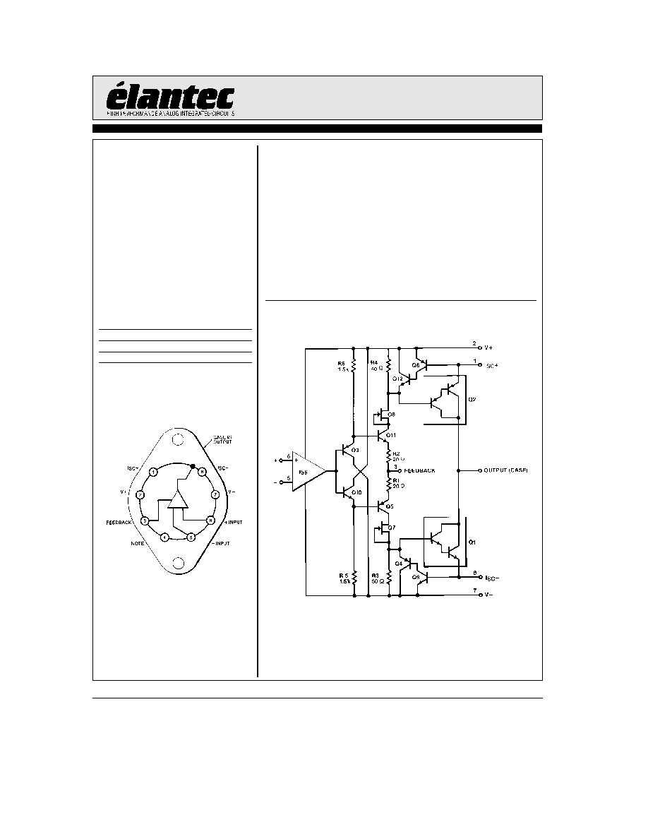
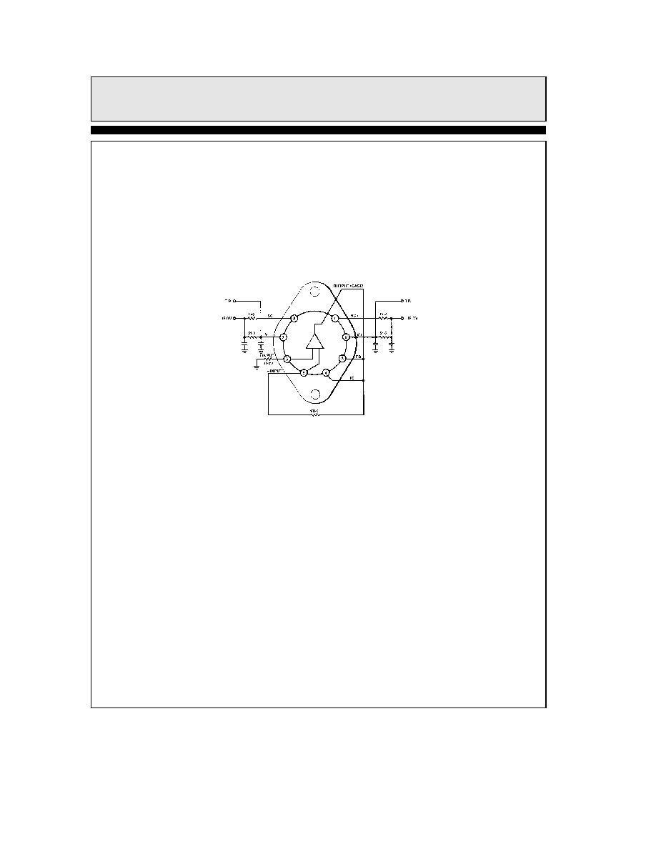
Connection Diagram
0101 ≠ 1
Top View
Note Electrically connected internally
No connection should be made to pin
General Description
The ELH0101 is a wideband power operational amplifier featur-
ing FET inputs internal compensation virtually no crossover
distortion and rapid settling time These features make the
ELH0101 an ideal choice for DC or AC servo amplifiers deflec-
tion yoke drivers programmable power supplies and disk head
positioner amplifiers
Elantec facilities comply with MIL-I-45208A and other applica-
ble quality specifications Elantec's Military devices are 100%
fabricated and assembled in our rigidly controlled ultra-clean
facilities in Milpitas California For additional information on
Elantec's Quality and Reliability Assurance policy and proce-
dures request brochure QRA-1
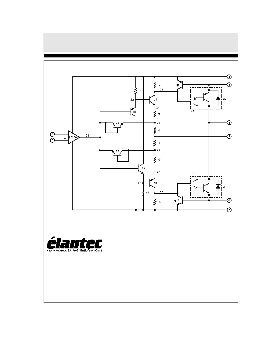
Equivalent Schematic
0101 ≠ 2
TAB
WIDE

ELH0101 883 8508901 2YX
Power Operational Amplifier
Absolute Maximum Ratings
V
S
Supply Voltage
ELH0101 ELH0101A
g
22V
P
D
Power Dissipation at T
A
e
25 C
5W
Derate linearly at 25 C W
to zero at 150 C
P
D
Power Dissipation at T
C
e
25 C
62W
Derate linearly at 2 C W
to zero at 150 C
Differential Input Voltage
ELH0101 ELH0101A
g
40V but
k g
V
S
V
IN
Input Voltage Range
ELH0101 ELH0101A
g
20V but
k g
V
S
Peak Output Current (50 ms pulse)
5A
Output Short Circuit Duration
(within rated power dissipation
R
SC
e
0 35
X T
A
e
25 C)
Continuous
T
A
Operating Temperature Range
ELH0101 ELH0101A
b
55 C to
a
125 C
T
J
Maximum Junction Temperature
150 C
T
ST
Storage Temperature
b
65 C to
a
150 C
Lead Temperature
(Soldering 10 seconds)
300 C
Important Note
All parameters having Min Max specifications are guaranteed The Test Level column indicates the specific device testing actually
performed during production and Quality inspection Elantec performs most electrical tests using modern high-speed automatic test
equipment specifically the LTX77 Series system Unless otherwise noted all tests are pulsed tests therefore T
J
e
T
C
e
T
A
Test Level
Test Procedure
I
100% production tested and QA sample tested per QA test plan QCX0002
II
100% production tested at T
A
e
25 C and QA sample tested at T
A
e
25 C
T
MAX
and T
MIN
per QA test plan QCX0002
III
QA sample tested per QA test plan QCX0002
IV
Parameter is guaranteed (but not tested) by Design and Characterization Data
V
Parameter is typical value at T
A
e
25 C for information purposes only
DC Electrical Characteristics
(Note 1) V
S
e
g
15V T
A
e
25 C V
CM
e
0V
Parameter
Description
Test Conditions
ELH0101
ELH0101A
Level
Test
Units
Min
Typ
Max
Min
Typ
Max
V
OS
Input Offset
1
10
1
3
I
mV
Voltage
T
MIN
s
T
A
s
T
MAX
15
7
I
mV
ELH0101
DV
OS
DP
D
Change in Input
(Note 2)
Offset Voltage with
150
150
V
mV W
Dissipated Power
DV
OS
DT
Change in Input
Offset Voltage with
10
10
V
mV C
Temperature
I
B
Input Bias Current
1 000
300
I
pA
T
A
s
T
MAX
1 000
300
I
nA
ELH0101
2
TD
is
23in
ELH0101 883 8508901 2YX
Power Operational Amplifier
DC Electrical Characteristics
(Note 1) V
S
e
g
15V T
A
e
25 C V
CM
e
0V
Contd
Parameter
Description
Test Conditions
ELH0101
ELH0101A
Level
Test
Units
Min
Typ
Max
Min
Typ
Max
I
OS
Input Offset
250
75
I
pA
Current
T
A
s
T
MAX
250
75
I
nA
ELH0101 A
A
VOL
Large Signal
V
O
e
g
10V R
L
e
10
X
50
200
50
200
I
V mV
Voltage Gain
V
O
Output Voltage
R
SC
e
0
X A
V
e
1
g
11 7
g
12 5
g
11 7
g
12 5
I
V
Swing
R
L
e
100
X (Note 3)
R
SC
e
0
X A
V
e
1
g
11
g
11 6
g
11
g
11 6
I
V
R
L
e
10
X (Note 3)
R
SC
e
0
X A
V
e
1
g
10 5
g
11
g
10 5
g
11
I
V
R
L
e
5
X (Note 3)
CMRR
Common-Mode
V
IN
e
g
10V
85
100
85
100
I
dB
Rejection Ratio
PSRR
Power Supply
g
5V
s
V
S
s g
15V
85
100
85
100
I
dB
Rejection Ratio
a
5V
s
V
S
(
a
)
s
a
15V
80
110
80
110
I
dB
V
S
(
b
)
e b
15V
b
5V
t
V
S
(
b
)
t
b
15V
80
95
80
95
I
dB
V
S
(
a
)
e a
15V
I
S
Supply Current
28
35
28
35
I
mA
AC Electrical Characteristics
V
S
e
g
15V T
A
e
T
C
e
T
J
e
25 C
Parameter
Description
Test Conditions
ELH0101
ELH0101A
Level
Test
Units
Min
Typ
Max
Min
Typ
Max
e
n
Equivalent Input
f
e
1 kHz
25
25
V
nV
0
Hz
Noise Voltage
C
IN
Input Capacitance
f
e
1 MHz
3
3
V
pF
PBW
Power Bandwidth
R
L
e
10
X A
V
e
1
300
300
V
kHz
b
3 dB
SR
Slew Rate
R
L
e
10
X A
V
e
1
7 5
10
7 5
10
I
V
ms
ELH0101AK
t
r
t
f
Small Signal Rise
R
L
e
10
X A
V
e
1
200
200
V
ns
or Fall Time
Small Signal
R
L
e
10
X A
V
e
1
10
10
V
%
Overshoot
3
TD
is
35in
TD
is
22in

ELH0101 883 8508901 2YX
Power Operational Amplifier
AC Electrical Characteristics
V
S
e
g
15V T
A
e
T
C
e
T
J
e
25 C
Contd
Parameter
Description
Test Conditions
ELH0101
ELH0101A
Level
Test
Units
Min
Typ
Max
Min
Typ
Max
GBW
Gain-Bandwidth
R
L
e
%
A
V
e
1
4
5
4
5
I
MHz
Product
ELH0101AK
t
S
Large Signal
Settling Time
R
L
e
%
A
V
e
1
2
2
V
ms
(0 01%)
THD
Total Harmonic
f
e
1 kHz P
O
e
0 5W
0 008
0 008
V
%
Distortion
R
L
e
10
X
Note 1 Specification is at T
A
e
25 C Actual values at operating temperature may differ from the T
A
e
25 C value When supply
voltages are
g
15V quiescent operating junction temperature will rise approximately 20 C without heatsinking Accordingly
V
OS
may change 0 5 mV and I
B
and I
OS
will change significantly during warm-ups Refer to I
B
vs temperature and power
dissipation graphs for expected values
Note 2 Change in offset voltage with dissipated power is due entirely to average device temperature rise and not to differential
thermal feedback effects Test is performed without any heatsink
Note 3 At light loads the output swing may be limited by the second stage rather than the output stage See the application section
under ``Output swing enhancement'' for hints on how to obtain extended operation R
SC
is the current sense resistor
4
TD
is
15in
ELH0101 883 8508901 2YX
Power Operational Amplifier
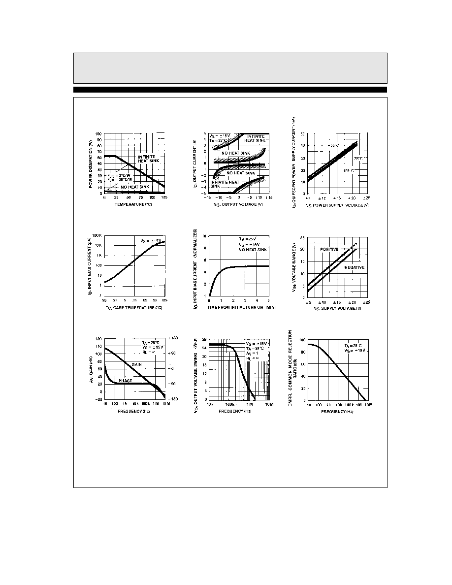
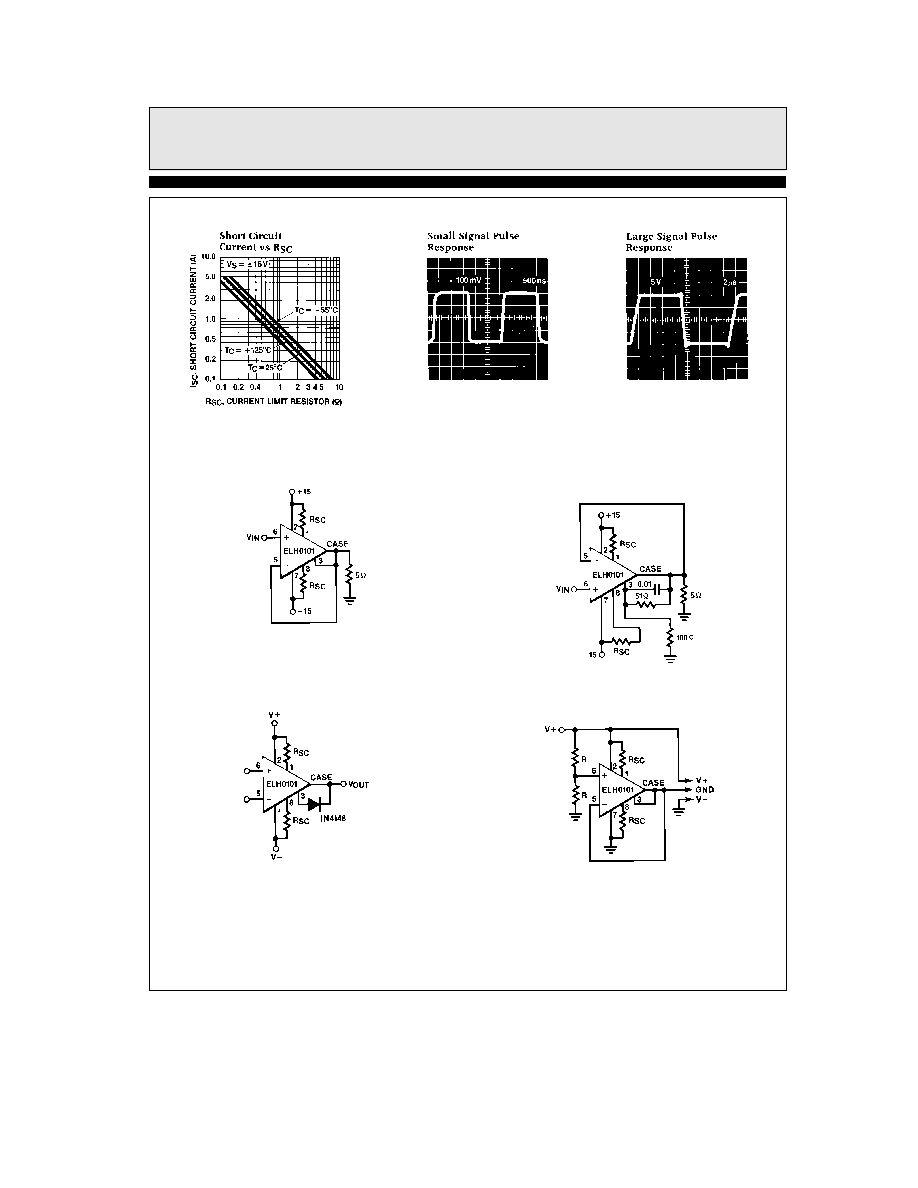
Typical Performance Curves
Power Dissipation
Safe Operating Area
Current
Quiescent Power Supply
Input Bias Current
Warm-up
Input Bias Current After
Voltage Range
Input Common-Mode
Frequency Response
Open-Loop Small Signal
Frequency
Output Voltage Swing vs
Ratio vs Frequency
Common-Mode Rejection
0101 ≠ 3
5
ELH0101 883 8508901 2YX
Power Operational Amplifier
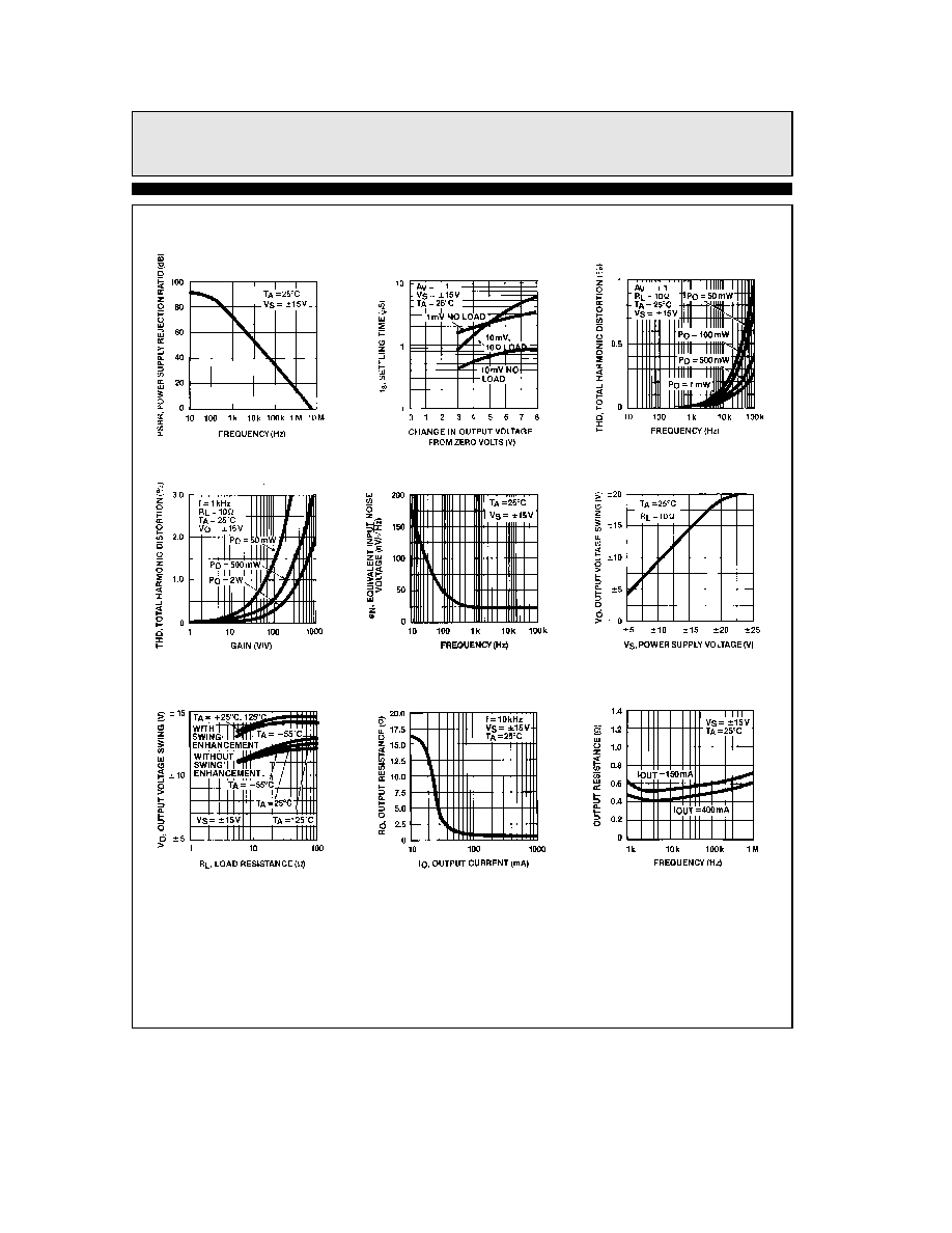
Typical Performance Curves
Contd
Ratio vs Frequency
Power Supply Rejection
Settling Time
vs Frequency
Total Harmonic Distortion
vs Gain
Total Harmonic Distortion
Voltage
Equivalent Input Noise
Swing Enhancement
Output Voltage Swing with
Load Resistance
Output Voltage Swing vs
Resistance
Open-Loop Output
Resistance vs Frequency
Open-Loop Output
0101 ≠ 4
6
ELH0101 883 8508901 2YX
Power Operational Amplifier
Typical Performance Curves
Contd
0101 ≠ 5
Typical Applications
High Power Voltage Follower
0101 ≠ 6
High Power Voltage Follower
with Swing Enhancement
0101 ≠ 7
Restricting Outputs to Positive Voltage Only
0101 ≠ 8
Generating a Split Supply
from a Single Voltage Supply
0101 ≠ 9
7
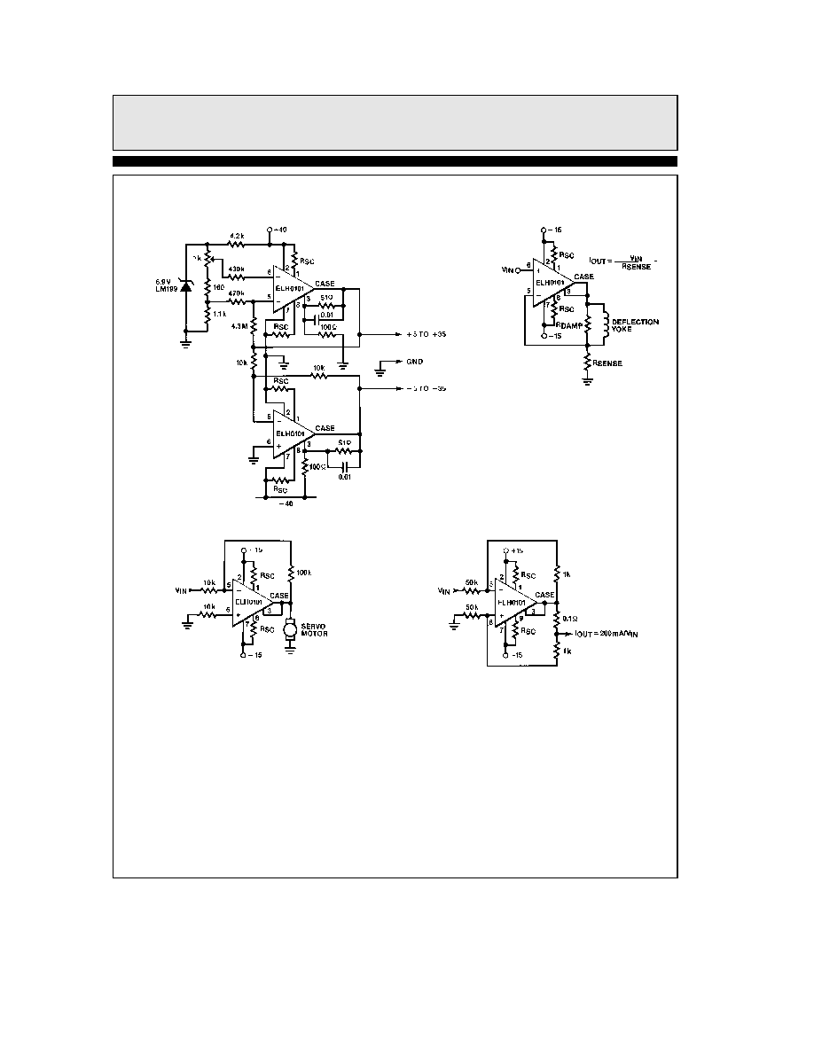
ELH0101 883 8508901 2YX
Power Operational Amplifier
Typical Applications
Contd
g
5 to
g
35 Power Source or Sink
0101 ≠ 10
CRT Deflection Yoke Driver
0101 ≠ 11
DC Servo Amplifier
0101 ≠ 12
High Current Source Sink
0101 ≠ 13
8

ELH0101 883 8508901 2YX
Power Operational Amplifier
Applications Information
Input Voltages
The ELH0101 operational amplifier contains
JFET input devices which exhibit high reverse
breakdown voltages from gate to source or drain
This eliminates the need for input clamp diodes
so that high differential input voltages may be
applied without a large increase in input current
However neither input voltage should be allowed
to exceed the negative supply as the resultant
high current flow may destroy the unit
Exceeding the negative common-mode limit on
either input will cause a reversal of the phase to
the output and force the amplifier output to the
corresponding high or low state Exceeding the
negative common-mode limit on both inputs will
force the amplifier output to a high state In nei-
ther case does a latch occur since raising the in-
put back within the common-mode range again
puts the input stage and thus the amplifier in a
normal operating mode
Exceeding the positive common-mode limit on a
single input will not change the phase of the out-
put however if both inputs exceed the limit the
output of the amplifier will be forced to a high
state
These amplifiers will operate with the common-
mode input voltage equal to the positive supply
In fact the common-mode voltage may exceed
the positive supply by approximately 100 mV in-
dependent of supply voltage and over the full op-
erating temperature range The positive supply
may therefore be used as a reference on an input
as for example in a supply current monitor and
or limiter
With the ELH0101 there is a temptation to re-
move the bias current compensation resistor nor-
mally used on the non-inverting input of a sum-
ming amplifier Direct connection of the inputs
to ground or a low-impedance voltage source is
not recommended with supply voltages greater
than 3V The potential problem involves loss of
one supply which can cause excessive current in
the second supply Destruction of the IC could
result if the current to the inputs of the device is
not limited to less than 100 mA or if there is
much more than 1
mF bypass on the supply bus
Although difficulties can be largely avoided by
installing clamp diodes across the supply lines on
every PC board a conservative design would in-
clude enough resistance in the input lead to limit
current to 10 mA if the input lead is pulled to
either supply by internal currents This precau-
tion is by no means limited to the ELH0101
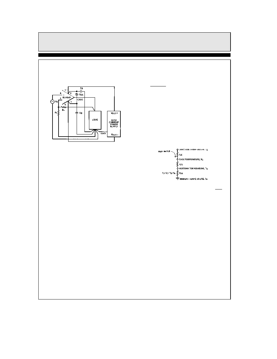
Layout Considerations
When working with circuitry capable of resolving
picoampere level signals leakage currents in cir-
cuitry external to the op amp can significantly
degrade performance High quality insulation is a
must (Kel-F and Teflon rate high) Proper clean-
ing of all insulating surfaces to remove fluxes and
other residues is also required This includes the
IC package as well as sockets and printed circuit
boards When operating in high humidity envi-
ronments or near 0 C some form of surface coat-
ing may be necessary to provide a moisture barri-
er
The effects of board leakage can be minimized by
encircling the input circuitry with a conductive
guard ring operated at a potential close to that of
the inputs
Electrostatic shielding of high impedance circuit-
ry is advisable
Error voltages can also be generated in the exter-
nal circuitry Thermocouples formed between dis-
similar metals can cause hundreds of microvolts
of error in the presence of temperature gradients
Since the ELH0101 can deliver large output cur-
rents careful attention should be paid to power
supply power supply bypassing and load cur-
rents Incorrect grounding of signal inputs and
load can cause significant errors
9
ELH0101 883 8508901 2YX
Power Operational Amplifier
Applications Information
Contd
Every attempt should be made to achieve a sin-
gle point ground system as shown in the figure
below
0101 ≠ 14
Bypass capacitor C
BX
should be used if the lead
lengths of bypass capacitors C
B
are long If a sin-
gle point ground system is not possible keep sig-
nal load and power supply from intermingling
as much as possible For further information on
proper grounding techniques refer to ``Grounding
and Shielding Techniques in Instrumentation''
by Morrison and ``Noise Reduction Techniques
in Electronic Systems'' by Ott (both published
by John Wiley and Sons)
Leads or PC board traces to the supply pins
short circuit current limit pins and the output
pin must be substantial enough to handle the
high currents that the ELH0101 is capable of
producing
Short Circuit Current Limiting
Should current limiting of the output not be nec-
essary SC
a
should be shorted to V
a
and SC
b
should be shorted to V
b
Remember that the
short circuit current limit is dependent upon the
total resistance seen between the supply and cur-
rent limit pins This total resistance includes the
desired resistor plus leads PC Board traces and
solder joints
Assuming a zero TCR current lim-
it resistor typical temperature coefficient of the
short circuit will be approximately 0 3%
Thermal Resistance
The thermal resistance between two points of a
conductive system is expressed as
i
12
e
T
1
b
T
2
P
D
C W
(1)
where subscript order indicates the direction of
heat flow A simplified heat transfer circuit for a
cased semiconductor and heatsink system is
shown in the figure below
The circuit is valid only if the system is in ther-
mal equilibrium (constant heat flow) and there
are indeed single specific temperatures T
J
T
C
and T
S
(no temperature distribution in junction
case or heatsink) Nevertheless this is a reason-
able approximation of actual performance
0101 ≠ 15
Short circuit current will be limited to approximately
0 6
RSC
The junction-to-case thermal resistance
i
JC
specified in the data sheet depends upon the ma-
terial and size of the package die size and thick-
ness and quality of the die bond to the case or
lead frame The case-to-heatsink thermal resist-
ance
i
CS
depends on the mounting of the device
to the heatsink and upon the area and quality of
the contact surface Typical
i
CS
for a TO-3 pack-
age is 0 5 C W to 0 7 C W
and 0 3 C W to
0 5 C W using silicone grease
The heatsink to ambient thermal resistance
i
SA
depends on the quality of the heatsink and the
ambient conditions
10
ELH0101 883 8508901 2YX
Power Operational Amplifier
Application Information
Contd
Cooling is normally required to maintain the
worst case operating junction temperature T
J
of
the device below the specified maximum value
T
J(MAX)
T
J
can be calculated from known oper-
ating conditions Rewriting equation (1) we find
i
JA
e
T
J
b
T
A
P
D
C W
T
J
e
T
A
a
P
D
i
JA
C
Where P
D
e
(V
S
b
V
OUT
) I
OUT
a
l
V
g
(V
b
)
l
I
Q
i
JA
e
i
JC
a
i
CS
a
i
SA
and
V
S
e
Supply Voltage
i
JC
for the ELH0101 is typically 2 C W
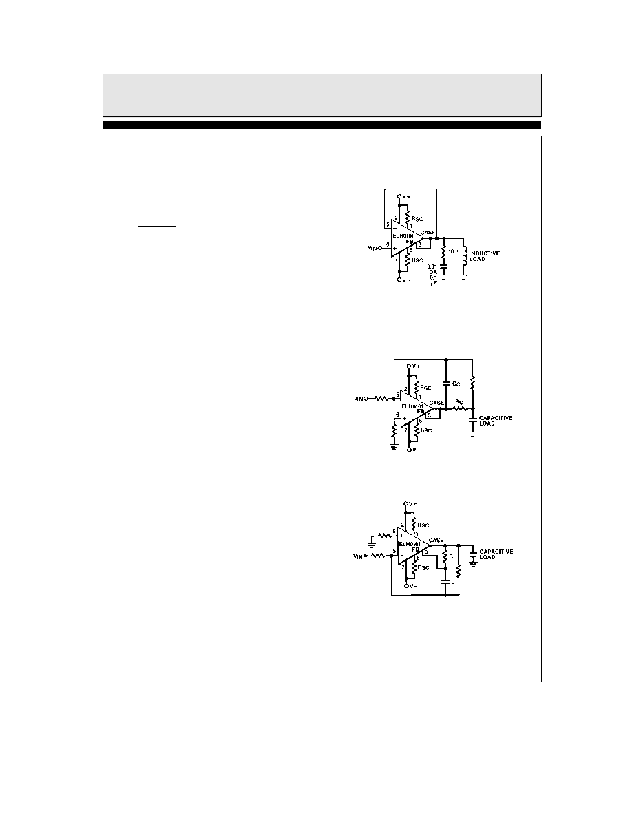
Stability and Compensation
As with most amplifiers care should be taken
with lead dress component placement and sup-
ply decoupling in order to ensure stability For
example resistors from the output to an input
should be placed with the body close to the input
to minimize ``pickup'' and maximize the frequen-
cy of the feedback pole by minimizing the capaci-
tance from the input to ground
A feedback pole is created when the feedback
around any amplifier is resistive The parallel re-
sistance and capacitance from the input of the
device (usually the inverting input) to AC
ground set the frequency of the pole In many
instances the frequency of this pole is much
greater than the expected 3 dB frequency of the
closed loop gain and consequently there is negli-
gible effect on stability margin However if the
feedback pole is less than approximately six
times the expected 3 dB frequency a lead capaci-
tor should be placed from the output to the input
of the op amp The value of the added capacitor
should be such that the RC time constant of this
capacitor and the resistance it parallels is greater
than or equal to the original feedback pole time
constant
Some inductive loads may cause output stage os-
cillation A 0 01
mF ceramic capacitor in series
with a 10
X resistor from the output to ground
will usually remedy this situation
0101 ≠ 16
Capacitive loads may be compensated for by tra-
ditional techniques (See ``Operational Amplifi-
ers Theory and Practice'' by Roberge published
by Wiley )
0101 ≠ 17
A similar but alternative technique may be used
for the ELH0101
0101 ≠ 18
11
ELH0101 883 8508901 2YX
Power Operational Amplifier
Output Swing Enhancement
When the feedback pin is connected directly to
the output the output voltage swing is limited
by the driver stage and not by output saturation
Output swing can be increased by taking gain in
the output stage as shown below in the High
Power Voltage Follower with Swing Enhance-
ment
Whenever gain is taken in the output
stage either the output stage or the entire op
amp must be appropriately compensated to ac-
count for the additional loop gain
Output Resistance
The open-loop output resistance of the ELH0101
is a function of the load current No-load output
resistance is approximately 10
X This decreases
to under an
X for load currents exceeding
100 mA
Burn-In Circuit
0101 ≠ 19
12

ELH0101 883 8508901 2YX
Power Operational Amplifier
ELH0101 Macromodel
Connections
a
input
l
b
Input
l
l
V
a
l
l
l
Isc
a
l
l
l
l
Feedback
l
l
l
l
l
V
b
l
l
l
l
l
l
Isc
b
l
l
l
l
l
l
l
Output
l
l
l
l
l
l
l
l
em0101
6
5
2
1
3
7
8
4
subckt buffer
21
2
1
3
7
8
4
Resistors
r1 3 27 10
r2 26 3 10
r3 30 7 50
r4 2 23 50
r5 29 7 2K
r6 2 22 2K
r7 27 28 10
r8 24 26 10
Transistors
q1 4 30 8 qnd
d1 8 4 dclamp
q2 4 23 1 qpd
d2 4 1 dclamp
q3 7 21 22 qp
q4 23 22 24 qn
q5 21 21 26 qn
q6 23 1 2 qp
q7 2 21 29 qn
q8 27 27 21 qn
q9 30 29 28 qp
q10 30 8 7 qn
Models
model qpd pnp (is
e
88 013e
b
12 ikf
e
5A tf
e
32nS vaf
e
50V cje
e
45pF cjc
e
60pF
a
xtb
e
2 1 bf
e
12000 ne
e
4 ise
e
1e
b
10)
model qnd npn (is
e
88 013e
b
12 ikf
e
5A tf
e
32nS vaf
e
50V cje
e
45pF cjc
e
60pF
a
xtb
e
2 1 bf
e
12000 ne
e
4 isc
e
1e
b
10)
model dclamp d (is
e
10e
b
28 tt
e
100nS)
13
TAB
WIDE
TD
is
52in

ELH0101 883 8508901 2YX
Power Operational Amplifier
ELH0101 Macromodel
Contd
model qp pnp (is
e
10e
b
15 xti
e
3 eg
e
1 11V vaf
e
91V bf
e
200 ne
e
2 321 ise
e
6 2fA
a
ikf
e
500mA xtb
e
2 1 br
e
3 3 nc
e
2 cjc
e
14 6pF vjc
e
0 75V mjc
e
0 3333 fc
e
0 5 cje
e
20pF
a
vje
e
0 75V mje
e
0 3333 tr
e
29nS tf
e
0 4nS itf
e
0 4 vtf
e
10 xtf
e
2 rb
e
10)
model qn npn (is
e
3e
b
15 xti
e
3 eg
e
1 11V vaf
e
151V bf
e
220 ne
e
1 541 ise
e
14fA
a
ikf
e
500mA xtb
e
2 1 br
e
6 nc
e
2 cjc
e
14 6pF vjc
e
0 75V mjc
e
0 3333 fc
e
0 5 cje
e
26pF
a
vje
e
0 75V mje
e
0 3333 tr
e
51nS tf
e
0 4nS itf
e
0 6 vtf
e
1 7 xtf
e
2 rb
e
10)
ends buffer
lf156 Subcircuit
Connections
a
Input
l
b
Input
l
l
V
a
l
l
l
V
b
l
l
l
l
Output
l
l
l
l
l
subckt lf156
6
5
2
7
21
Input Stage
vcm2 40 7 2
rd1 40 80 1 06K
rd2 40 90 1 06K
j1 80 102 12 jm1
j2 90 103 12 jm2
cin 5 6 4pF
rg1 5 102 2
rg2 6 103 2
CM Clamp
dcm1 107 103 dm4
dcm2 105 107 dm4
vcmc 105 7 4V
ecmp 106 7 103 7 1
rcmp 107 106 10K
dcm3 109 102 dm4
dcm4 105 109 dm4
ecmn 108 2 102 2 1
rcmn 109 108 10K
cl 80 90 15pF
iss 2 12 0 48mA
gosit 2 12 90 80 2 4e
b
4
Intermediate Stage
gcm 0 88 12 0 9 425e
b
9
ga 88 0 80 90 9 425e
b
4
r2 88 0 100K
c2 91 88 30pF
gb 91 0 88 0 28 6
ro2 91 0 74
14
TAB
WIDE
TD
is
58in

ELH0101 883 8508901 2YX
Power Operational Amplifier
ELH0101 Macromodel
Contd
Output Stage
rso 91 21 1
ecl 18 0 91 21 20 69
gcl 0 88 20 0 1
rcl 20 0 1K
d1 18 20 dm1
d2 20 18 dm1
d3a 131 70 dm3
d3b 13 131 dm3
gpl 0 88 70 2 1
vc 13 21 3 1552V
rpla 2 70 10K
rplb 2 131 100K
d4a 60 141 dm3
d4b 141 14 dm3
gnl 0 88 60 7 1
ve 21 14 3 1552V
rnla 60 7 10K
rnlb 141 7 100K
ip 2 7 4 52mA
dsub 7 2 dm2
Models
model jm1 pjf (is
e
3 15e
b
11 beta
e
9 2528e
b
4 vto
e b
1 0)
model jm2 pjf (is
e
2 85e
b
11 beta
e
9 2528e
b
4 vto
e b
0 999)
model dm1 d (is
e
1 0e
b
15)
model dm2 d (is
e
8 0e
b
16 bv
e
52 8)
model dm3 d (is
e
1 0e
b
16)
model dm4 d (is
e
1 0e
b
9)
ends lf156
lf156 model courtesy of Linear Technology Corp
15
TD
is
39in
ELH010188385089012YX
December
1994
Rev
H
ELH0101 883 8508901 2YX
Power Operational Amplifier
ELH0101 Macromodel
Contd
0101 ≠ 20
General Disclaimer
Specifications contained in this data sheet are in effect as of the publication date shown Elantec Inc reserves the right to make changes
in the circuitry or specifications contained herein at any time without notice Elantec Inc assumes no responsibility for the use of any
circuits described herein and makes no representations that they are free from patent infringement
Elantec Inc
1996 Tarob Court
Milpitas CA 95035
Telephone (408) 945-1323
(800) 333-6314
Fax (408) 945-9305
European Office 44-71-482-4596
WARNING
Life Support Policy
Elantec Inc products are not authorized for and should not be
used within Life Support Systems without the specific written
consent of Elantec Inc Life Support systems are equipment in-
tended to support or sustain life and whose failure to perform
when properly used in accordance with instructions provided can
be reasonably expected to result in significant personal injury or
death Users contemplating application of Elantec Inc products
in Life Support Systems are requested to contact Elantec Inc
factory headquarters to establish suitable terms
conditions for
these applications Elantec Inc 's warranty is limited to replace-
ment of defective components and does not cover injury to per-
sons or property or other consequential damages
Printed in U S A
16