 | –≠–ª–µ–∫—Ç—Ä–æ–Ω–Ω—ã–π –∫–æ–º–ø–æ–Ω–µ–Ω—Ç: ELH0101A | –°–∫–∞—á–∞—Ç—å:  PDF PDF  ZIP ZIP |
ELH010188385089012YX
December
1994
Rev
H
ELH0101 883 8508901 2YX
Power Operational Amplifier
Note All information contained in this data sheet has been carefully checked and is believed to be accurate as of the date of publication however this data sheet cannot be a ``controlled document'' Current revisions if any to these
specifications are maintained at the factory and are available upon your request We recommend checking the revision level before finalization of your design documentation Patent pending
1985 Elantec Inc
Features
5A peak 2A continuous output
current
10 V ms slew rate
300 kHz power bandwidth
850 mW standby power (
g
15V
supplies)
300 pA input bias current
Virtually no crossover distortion
2 ms settling time to 0 01%
5 MHz gain bandwidth
MIL-STD-883 devices 100%
manufactured in U S A
Ordering Information
Part No
Temp Range Package Outline
ELH0101AK 883B
b
55 C to
a
125 C
TO-3
MDP0003
ELH0101K 883B
b
55 C to
a
125 C
TO-3
MDP0003
8508901YX and 8508902YX are the SMD
versions of this device
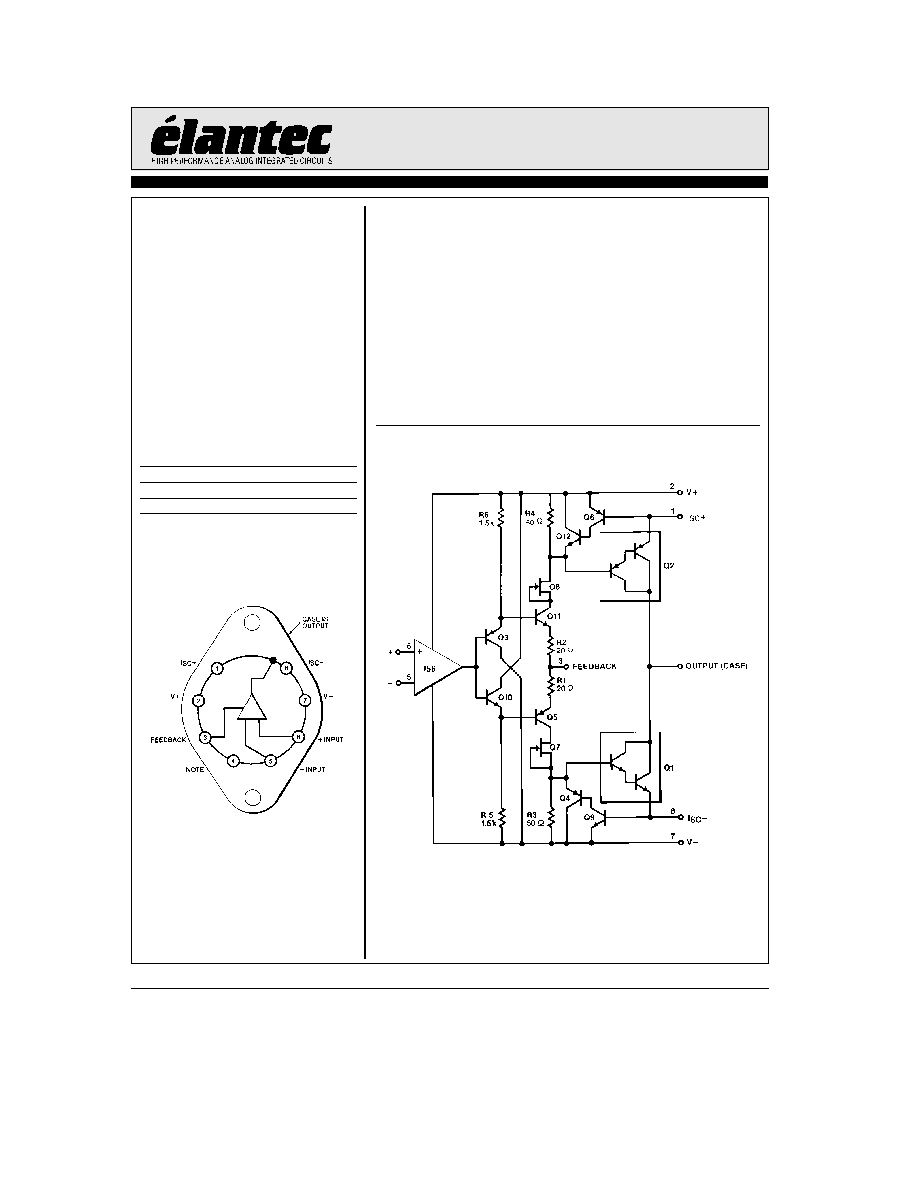
Connection Diagram
0101 ≠ 1
Top View
Note Electrically connected internally
No connection should be made to pin
General Description
The ELH0101 is a wideband power operational amplifier featur-
ing FET inputs internal compensation virtually no crossover
distortion and rapid settling time These features make the
ELH0101 an ideal choice for DC or AC servo amplifiers deflec-
tion yoke drivers programmable power supplies and disk head
positioner amplifiers
Elantec facilities comply with MIL-I-45208A and other applica-
ble quality specifications Elantec's Military devices are 100%
fabricated and assembled in our rigidly controlled ultra-clean
facilities in Milpitas California For additional information on
Elantec's Quality and Reliability Assurance policy and proce-
dures request brochure QRA-1
Equivalent Schematic
0101 ≠ 2
TAB
WIDE
ELH0101 883 8508901 2YX
Power Operational Amplifier
Absolute Maximum Ratings
V
S
Supply Voltage
ELH0101 ELH0101A
g
22V
P
D
Power Dissipation at T
A
e
25 C
5W
Derate linearly at 25 C W
to zero at 150 C
P
D
Power Dissipation at T
C
e
25 C
62W
Derate linearly at 2 C W
to zero at 150 C
Differential Input Voltage
ELH0101 ELH0101A
g
40V but
k g
V
S
V
IN
Input Voltage Range
ELH0101 ELH0101A
g
20V but
k g
V
S
Peak Output Current (50 ms pulse)
5A
Output Short Circuit Duration
(within rated power dissipation
R
SC
e
0 35
X T
A
e
25 C)
Continuous
T
A
Operating Temperature Range
ELH0101 ELH0101A
b
55 C to
a
125 C
T
J
Maximum Junction Temperature
150 C
T
ST
Storage Temperature
b
65 C to
a
150 C
Lead Temperature
(Soldering 10 seconds)
300 C
Important Note
All parameters having Min Max specifications are guaranteed The Test Level column indicates the specific device testing actually
performed during production and Quality inspection Elantec performs most electrical tests using modern high-speed automatic test
equipment specifically the LTX77 Series system Unless otherwise noted all tests are pulsed tests therefore T
J
e
T
C
e
T
A
Test Level
Test Procedure
I
100% production tested and QA sample tested per QA test plan QCX0002
II
100% production tested at T
A
e
25 C and QA sample tested at T
A
e
25 C
T
MAX
and T
MIN
per QA test plan QCX0002
III
QA sample tested per QA test plan QCX0002
IV
Parameter is guaranteed (but not tested) by Design and Characterization Data
V
Parameter is typical value at T
A
e
25 C for information purposes only
DC Electrical Characteristics
(Note 1) V
S
e
g
15V T
A
e
25 C V
CM
e
0V
Parameter
Description
Test Conditions
ELH0101
ELH0101A
Level
Test
Units
Min
Typ
Max
Min
Typ
Max
V
OS
Input Offset
1
10
1
3
I
mV
Voltage
T
MIN
s
T
A
s
T
MAX
15
7
I
mV
ELH0101
DV
OS
DP
D
Change in Input
(Note 2)
Offset Voltage with
150
150
V
mV W
Dissipated Power
DV
OS
DT
Change in Input
Offset Voltage with
10
10
V
mV C
Temperature
I
B
Input Bias Current
1 000
300
I
pA
T
A
s
T
MAX
1 000
300
I
nA
ELH0101
2
TD
is
23in
ELH0101 883 8508901 2YX
Power Operational Amplifier
DC Electrical Characteristics
(Note 1) V
S
e
g
15V T
A
e
25 C V
CM
e
0V
Contd
Parameter
Description
Test Conditions
ELH0101
ELH0101A
Level
Test
Units
Min
Typ
Max
Min
Typ
Max
I
OS
Input Offset
250
75
I
pA
Current
T
A
s
T
MAX
250
75
I
nA
ELH0101 A
A
VOL
Large Signal
V
O
e
g
10V R
L
e
10
X
50
200
50
200
I
V mV
Voltage Gain
V
O
Output Voltage
R
SC
e
0
X A
V
e
1
g
11 7
g
12 5
g
11 7
g
12 5
I
V
Swing
R
L
e
100
X (Note 3)
R
SC
e
0
X A
V
e
1
g
11
g
11 6
g
11
g
11 6
I
V
R
L
e
10
X (Note 3)
R
SC
e
0
X A
V
e
1
g
10 5
g
11
g
10 5
g
11
I
V
R
L
e
5
X (Note 3)
CMRR
Common-Mode
V
IN
e
g
10V
85
100
85
100
I
dB
Rejection Ratio
PSRR
Power Supply
g
5V
s
V
S
s g
15V
85
100
85
100
I
dB
Rejection Ratio
a
5V
s
V
S
(
a
)
s
a
15V
80
110
80
110
I
dB
V
S
(
b
)
e b
15V
b
5V
t
V
S
(
b
)
t
b
15V
80
95
80
95
I
dB
V
S
(
a
)
e a
15V
I
S
Supply Current
28
35
28
35
I
mA
AC Electrical Characteristics
V
S
e
g
15V T
A
e
T
C
e
T
J
e
25 C
Parameter
Description
Test Conditions
ELH0101
ELH0101A
Level
Test
Units
Min
Typ
Max
Min
Typ
Max
e
n
Equivalent Input
f
e
1 kHz
25
25
V
nV
0
Hz
Noise Voltage
C
IN
Input Capacitance
f
e
1 MHz
3
3
V
pF
PBW
Power Bandwidth
R
L
e
10
X A
V
e
1
300
300
V
kHz
b
3 dB
SR
Slew Rate
R
L
e
10
X A
V
e
1
7 5
10
7 5
10
I
V
ms
ELH0101AK
t
r
t
f
Small Signal Rise
R
L
e
10
X A
V
e
1
200
200
V
ns
or Fall Time
Small Signal
R
L
e
10
X A
V
e
1
10
10
V
%
Overshoot
3
TD
is
35in
TD
is
22in

ELH0101 883 8508901 2YX
Power Operational Amplifier
AC Electrical Characteristics
V
S
e
g
15V T
A
e
T
C
e
T
J
e
25 C
Contd
Parameter
Description
Test Conditions
ELH0101
ELH0101A
Level
Test
Units
Min
Typ
Max
Min
Typ
Max
GBW
Gain-Bandwidth
R
L
e
%
A
V
e
1
4
5
4
5
I
MHz
Product
ELH0101AK
t
S
Large Signal
Settling Time
R
L
e
%
A
V
e
1
2
2
V
ms
(0 01%)
THD
Total Harmonic
f
e
1 kHz P
O
e
0 5W
0 008
0 008
V
%
Distortion
R
L
e
10
X
Note 1 Specification is at T
A
e
25 C Actual values at operating temperature may differ from the T
A
e
25 C value When supply
voltages are
g
15V quiescent operating junction temperature will rise approximately 20 C without heatsinking Accordingly
V
OS
may change 0 5 mV and I
B
and I
OS
will change significantly during warm-ups Refer to I
B
vs temperature and power
dissipation graphs for expected values
Note 2 Change in offset voltage with dissipated power is due entirely to average device temperature rise and not to differential
thermal feedback effects Test is performed without any heatsink
Note 3 At light loads the output swing may be limited by the second stage rather than the output stage See the application section
under ``Output swing enhancement'' for hints on how to obtain extended operation R
SC
is the current sense resistor
4
TD
is
15in
ELH0101 883 8508901 2YX
Power Operational Amplifier
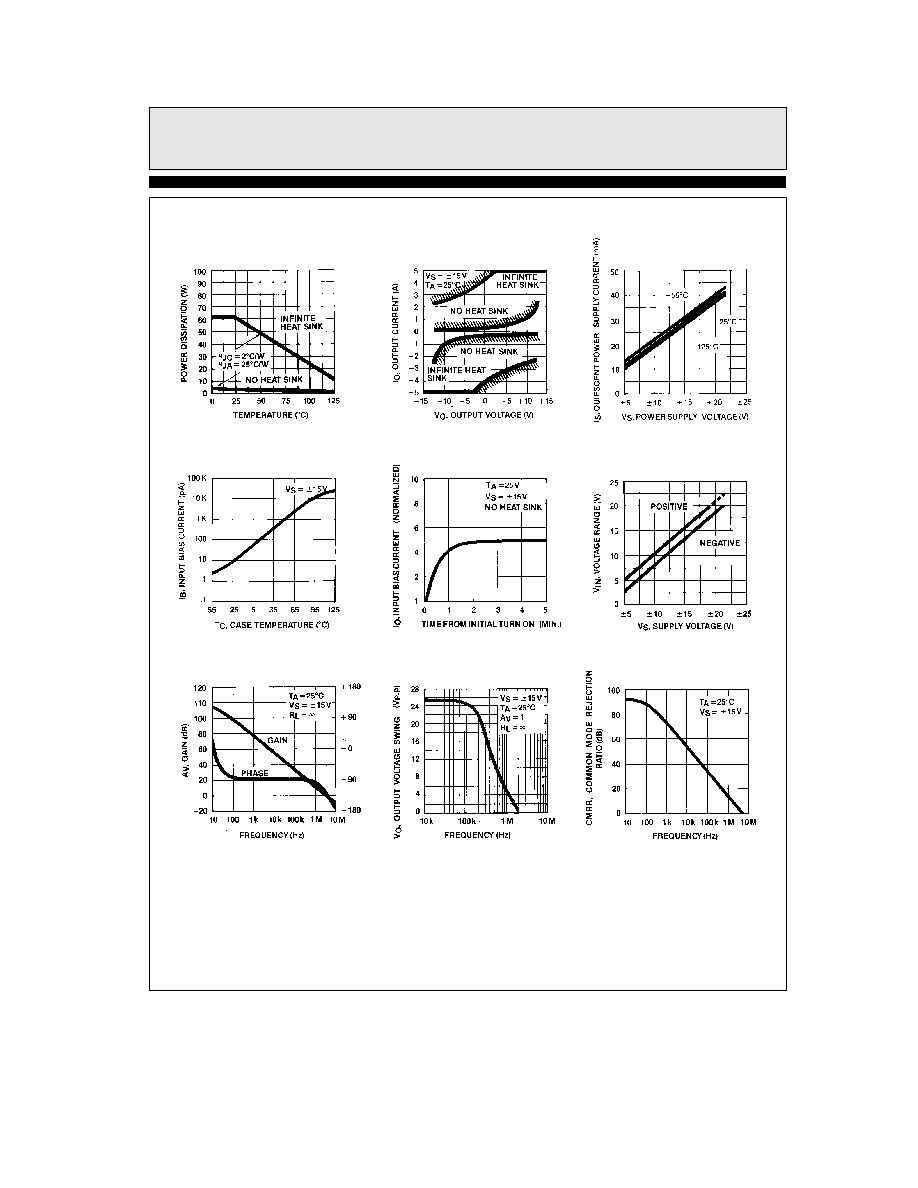
Typical Performance Curves
Power Dissipation
Safe Operating Area
Current
Quiescent Power Supply
Input Bias Current
Warm-up
Input Bias Current After
Voltage Range
Input Common-Mode
Frequency Response
Open-Loop Small Signal
Frequency
Output Voltage Swing vs
Ratio vs Frequency
Common-Mode Rejection
0101 ≠ 3
5