 | –≠–ª–µ–∫—Ç—Ä–æ–Ω–Ω—ã–π –∫–æ–º–ø–æ–Ω–µ–Ω—Ç: K75-83 | –°–∫–∞—á–∞—Ç—å:  PDF PDF  ZIP ZIP |
159
K75-83
______________________________________________________________________________________________
PAPER ≠ METALLIZER FILM CAPACITORS
,
,
.
75-81.
.
:
.
Designed to operate in DC, AC and ripple
current circuits and in pulse mode.
Designed for higher frequency than K75-
81.
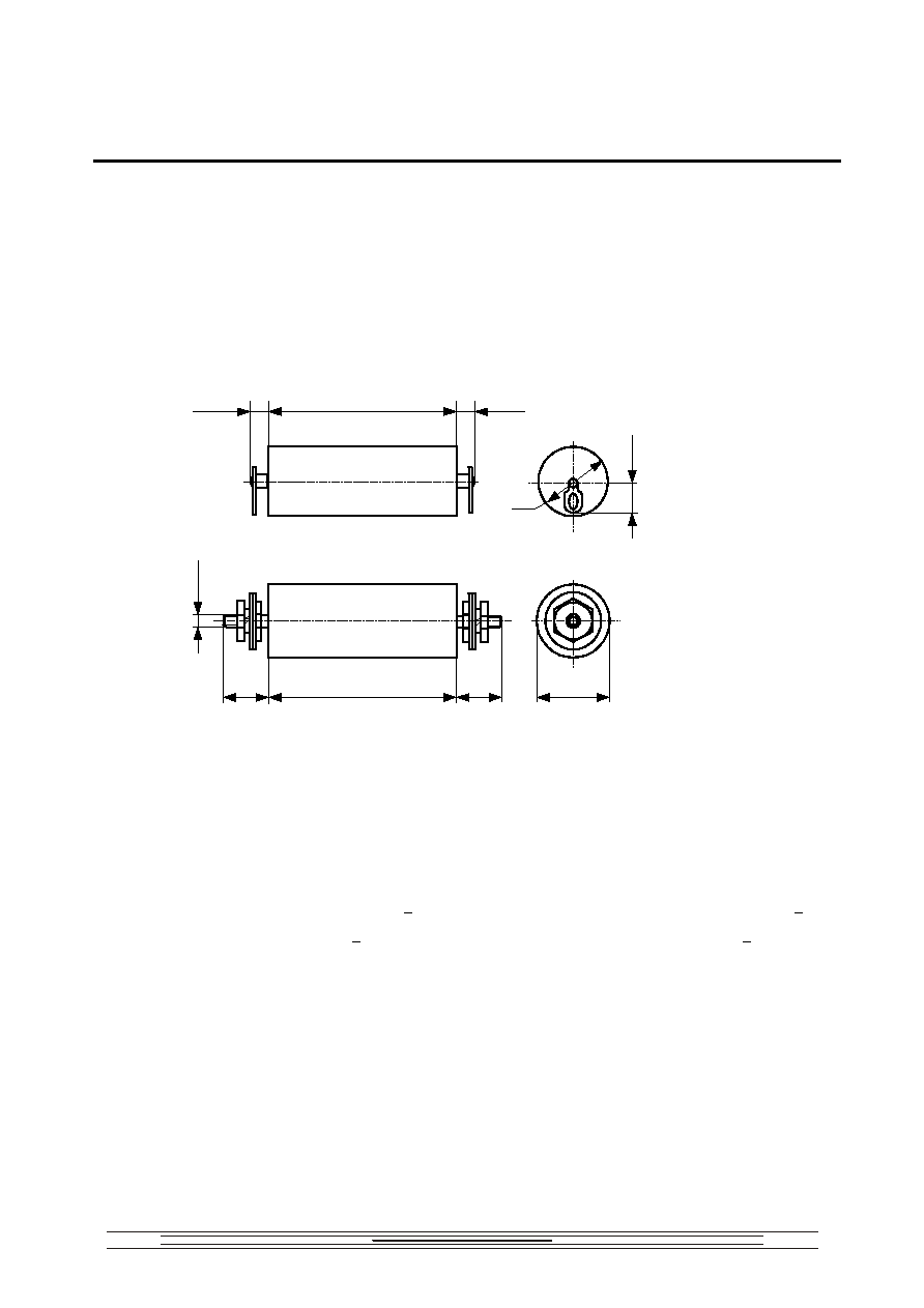
Design:
cylindrical housing made of
polymeric materials. Axial terminals
.
" "
Design " "
L
12
max
12
max
12±
1
L
25
max
25
max
M6-
6g
D
D
" "
Design "b"
2,0...100
Rated capacitance
2.0...100 F
1,0...6,3
Rated voltage
1.0...6.3 kV
±10%
Capacitance tolerance
±10%
f = 1
<0,004
Dissipation factor at f = 1 kHz
<0.004
> 500
.
Time constant
> 500 MOhm.F
-60...+50
o
C
Operating
temperature
range
-60...+50
o
C
5,0...50
Pulse repetition frequency
5.0...50 Hz
75...5000 A
Discharge current amplitude
75...5000 A
10
Shelf life
10 years
:
75-83 - 5
- 20
±10%
Ordering example:
Capacitor K75-83b ≠ 5 kV ≠ 20 F ± 10%
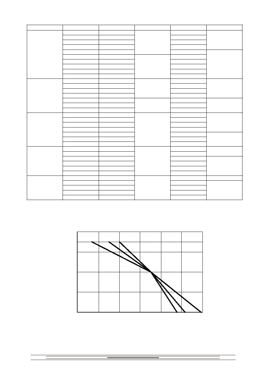
160
Ur, V
Cr,
F
D max, mm
L max, mm
Mass, g max
Design
2
20
30
4
25
45
6
30
65
8
34
85
a
10
38
75
100
20
36
180
40
48
300
60
58
450
80
67
600
1000
100
75
140
750
a, b
2 27
60
4 36
110
6 42
145
8 49
75
200
a
10 38
230
20 53
440
2000
40 73
140
820
a, b
2 23
90
4 30
145
6 37
220
8 42
275
a
10 48
360
20
65
650
3000
40
92
140
1300
a, b
2 37
220
4 50
390
a
6 62
600
8 70
760
10 78
950
5000
20
110
140
1900
a, b
2 42
275 a
4 60
560
6 73
820
8 82
1000
6300
10 92
140
1300
a, b
T=40
o
C
Minimum operating time as a function of voltage at T=40
o
C
lg
(lg N)
4.0 (6.5)
3.5 (6)
2.5 (5)
1.5 (4)
0.5 (3)
0.3
0.5
0.7
0.9
1.1
1.3
1.5
U / Ur
1
1
2
2
3
3
-
; N -
- in hours; N - number of pulses
1) Ur = 1000 B
2) Ur = 2000 B; 3000 B
3) Ur = 5000 B; 6300 B
1) Ur = 1000 V
2) Ur = 2000 V; 3000 V
3) Ur = 5000 V; 6300 V
161
U
2
m
CF tg
g
+2( U
m
FC)
2
R
A
< 20 / R
T
,
R
T
, tg
g
, R
A
-
,
:
Permissible amplitude of AC sinusoidal component of voltage at amb is expressed by
U
2
m
CF tg
g
+2( U
m
FC)
2
R
A
< 20 / R
T
,
where
R
T
, tg
g
, R
A
-
are parameters given in the table:
Ur, V
Cr, F
R
A
*10
3
, Ohm
R
T
,
o
C/W
t
g
g
*10
4
Design
2
27 33
4
16 25
6
11 21
8
8 19
a
10
7 17
20
15 10
40
8 8
60
6 7
80
4 6
1000
100
3 6
a, b
2
25 24
4
13 18
6
10 15
8
7 13
a
10
24 9
20
12 7
2000
40
6 6
a, b
2
88 15
4
49 11
6
31 10
8
24 9
a
10
18 8
20
10 6
3000
40
5 5
a, b
2
55 10
4
29 8
a
6
19 7
8
15 6
10
12 5
5000
20
6 4
a, b
2
48 9
a
4
23 7
6
15 6
8
12 5
6300
10
10 5
20
a, b
:
Permissible parameters of pulse mode must not exceed the values calculated from the following
formulas:
T
A
r
r
R
R
F
C
U
F
F
C
U
/
20
/
2
.
1
8
.
1
lg
10
4
.
2
2
2
2
4
,
,
1
.
1
0
I
F
C
U
r
Im < Im
max
162
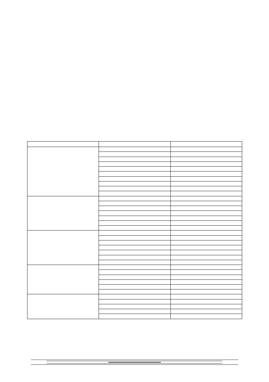
U -
,
;
F -
,
;
≠
, .
I
0
= 25 ≠
"a";
I
0
= 40 ≠
"b";
Im -
Im
max
-
(
).
where
U - amplitude of peak-to-peak pulse voltage, V;
F - pulse repetition rate;
≠ discharge current pulse duration, s;
I
0
= 25 ≠ for design "a";
I
0
= 40 ≠ for design "b";
Im - discharge current amplitude
Im
max
- Max. discharge current amplitude that is given in the table below
,
Max. discharge current amplitude, A
Ur, V
Cr,
F
Im, A
2
100
4
170
6
220
8
320
10
430
20
380
40
1100
60
1100
80
1100
1000
100
2300
2 120
4 340
6 340
8 570
10 350
20 600
2000
40 1043
2 200
4 300
6 400
8 400
10 500
20
1100
3000
40
1100
2 100
4 200
6 300
8 450
10 550
5000
20
1100
2 270
4 600
6 900
8 1100
6300
10 1500