Document Outline
- COVER
- Description
- Features
- Ordering Information
- Pin Configurations
- Pin Description
- Serial PD Matrix
- Block Diagram
- Logical Clock Net Structure
- Electrical Specifications
- Absolute Maximum Ratings
- DC Operating Conditions
- DC Characteristics 1
- AC Timing for IDD Test Conditions
- DC Characteristics 2
- DC Characteristics 3
- ODT DC Electrical Characteristics
- OCD Default Characteristics
- Pin Capacitance
- AC Characteristics
- ODT AC Electrical Characteristics
- Pin Functions
- Detailed Operation Part and Timing Waveforms
- Physical Outline

Document No. E0721E10 (Ver. 1.0)
Date Published May 2005 (K) Japan
Printed in Japan
URL: http://www.elpida.com
Elpida Memory, Inc. 2005
DATA SHEET
1GB Unbuffered DDR2 SDRAM DIMM
EBE11UD8AEFA-6
(128M words
◊
64 bits, 2 Ranks)
Description
The EBE11UD8AEFA is 128M words
◊
64 bits, 2 ranks
DDR2 SDRAM unbuffered module, mounting 16 pieces
of 512M bits DDR2 SDRAM sealed in FBGA (
µ
BGA
)
package. Read and write operations are performed at
the cross points of the CK and the /CK. This high-
speed data transfer is realized by the 4 bits prefetch-
pipelined architecture. Data strobe (DQS and /DQS)
both for read and write are available for high speed and
reliable data bus design. By setting extended mode
register, the on-chip Delay Locked Loop (DLL) can be
set enable or disable. This module provides high
density mounting without utilizing surface mount
technology. Decoupling capacitors are mounted
beside each FBGA (
µ
BGA) on the module board.
Note: Do not push the components or drop the
modules in order to avoid mechanical defects,
which may result in electrical defects.
Features
∑
240-pin socket type dual in line memory module
(DIMM)
PCB height: 30.0mm
Lead pitch: 1.0mm
Lead-free
∑
Power supply: VDD
=
1.8V
±
0.1V
∑
Data rate: 667Mbps (max.)
∑
SSTL_18 compatible I/O
∑
Double-data-rate architecture: two data transfers per
clock cycle
∑
Bi-directional, differential data strobe (DQS and
/DQS) is transmitted/received with data, to be used in
capturing data at the receiver
∑
DQS is edge aligned with data for READs: center-
aligned with data for WRITEs
∑
Differential clock inputs (CK and /CK)
∑
DLL aligns DQ and DQS transitions with CK
transitions
∑
Commands entered on each positive CK edge: data
and data mask referenced to both edges of DQS
∑
Four internal banks for concurrent operation
(components)
∑
Data mask (DM) for write data
∑
Burst lengths: 4, 8
∑
/CAS Latency (CL): 3, 4, 5
∑
Auto precharge operation for each burst access
∑
Auto refresh and self refresh modes
∑
Average refresh period
7.8
µ
s at 0
∞
C
TC
+
85
∞
C
3.9
µ
s at
+
85
∞
C
<
TC
+
95
∞
C
∑
Posted CAS by programmable additive latency for
better command and data bus efficiency
∑
Off-Chip-Driver Impedance Adjustment and On-Die-
Termination for better signal quality
∑
/DQS can be disabled for single-ended Data Strobe
operation
EBE11UD8AEFA-6
Data Sheet E0721E10 (Ver. 1.0)
2
Ordering Information
Part number
Data rate
Mbps (max.)
Component
JEDEC speed bin
(CL-tRCD-tRP)
Package
Contact
pad
Mounted devices
EBE11UD8AEFA-6E-E 667
DDR2-667 (5-5-5)
240-pin DIMM
(lead-free)
Gold EDE5108AESK-6E-E
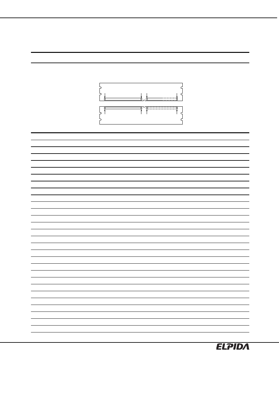
Pin Configurations
1 pin
Front side
Back side
64 pin 65 pin
120 pin
121 pin
184 pin 185 pin
240 pin
Pin No.
Pin name
Pin No.
Pin name
Pin No.
Pin name
Pin No.
Pin name
1 VREF
61 A4 121 VSS 181 VDD
2 VSS 62 VDD 122 DQ4 182 A3
3 DQ0 63 A2 123 DQ5 183 A1
4 DQ1 64 VDD 124 VSS 184 VDD
5 VSS 65 VSS 125 DM0 185 CK0
6 /DQS0
66 VSS 126 NC 186 /CK0
7 DQS0
67 VDD 127 VSS 187 VDD
8 VSS 68 NC 128 DQ6 188 A0
9 DQ2 69 VDD 129 DQ7 189 VDD
10 DQ3 70 A10/AP
130 VSS 190 BA1
11 VSS 71 BA0 131 DQ12 191 VDD
12 DQ8 72
VDD 132 DQ13 192 /RAS
13 DQ9 73 /WE 133 VSS 193 /CS0
14 VSS 74 /CAS 134 DM1 194 VDD
15 /DQS1
75 VDD 135 NC 195 ODT0
16 DQS1 76 /CS1 136 VSS 196 A13
17 VSS 77 ODT1 137 CK1 197 VDD
18 NC 78 VDD 138 /CK1 198 VSS
19 NC 79 VSS 139 VSS 199 DQ36
20 VSS 80
DQ32 140 DQ14 200 DQ37
21 DQ10 81
DQ33 141 DQ15 201 VSS
22 DQ11
82 VSS 142 VSS 202 DM4
23 VSS 83 /DQS4
143 DQ20 203 NC
24 DQ16 84 DQS4 144 DQ21 204 VSS
25 DQ17
85 VSS 145 VSS 205 DQ38
26 VSS 86 DQ34 146 DM2 206 DQ39
27 /DQS2
87 DQ35 147 NC 207 VSS
28 DQS2
88 VSS 148 VSS 208 DQ44
29 VSS 89
DQ40 149 DQ22 209 DQ45

EBE11UD8AEFA-6
Data Sheet E0721E10 (Ver. 1.0)
3
Pin No.
Pin name
Pin No.
Pin name
Pin No.
Pin name
Pin No.
Pin name
30 DQ18 90
DQ41 150 DQ23 210 VSS
31 DQ19
91 VSS 151 VSS 211 DM5
32 VSS 92 /DQS5
152 DQ28 212 NC
33 DQ24 93 DQS5 153 DQ29 213 VSS
34 DQ25
94 VSS 154 VSS 214 DQ46
35 VSS 95 DQ42 155 DM3 215 DQ47
36 /DQS3
96 DQ43 156 NC 216 VSS
37 DQS3
97 VSS 157 VSS 217 DQ52
38 VSS 98
DQ48 158 DQ30 218 DQ53
39 DQ26 99
DQ49 159 DQ31 219 VSS
40 DQ27
100 VSS 160 VSS 220 CK2
41 VSS 101 SA2 161 NC 221 /CK2
42
NC 102 NC 162 NC 222 VSS
43 NC 103 VSS 163 VSS 223 DM6
44 VSS 104 /DQS6
164 NC 224 NC
45 NC 105 DQS6 165 NC 225 VSS
46 NC 106 VSS
166 VSS 226 DQ54
47 VSS 107 DQ50 167 NC 227 DQ55
48 NC 108 DQ51 168 NC 228 VSS
49 NC 109 VSS 169 VSS 229 DQ60
50 VSS 110 DQ56 170 VDD 230 DQ61
51 VDD 111 DQ57 171 CKE1 231 VSS
52 CKE0 112 VSS 172 VDD 232 DM7
53 VDD 113 /DQS7
173 NC 233 NC
54 NC 114 DQS7 174 NC 234 VSS
55 NC 115 VSS 175 VDD 235 DQ62
56 VDD 116 DQ58 176 A12 236 DQ63
57 A11 117 DQ59 177 A9 237 VSS
58 A7 118 VSS 178 VDD 238 VDDSPD
59 VDD 119 SDA 179 A8 239 SA0
60 A5 120 SCL 180 A6 240 SA1
EBE11UD8AEFA-6
Data Sheet E0721E10 (Ver. 1.0)
4
Pin Description
Pin name
Function
A0 to A13
Address input
Row address
A0 to A13
Column address
A0 to A9
A10 (AP)
Auto precharge
BA0, BA1
Bank select address
DQ0 to DQ63
Data input/output
/RAS
Row address strobe command
/CAS
Column address strobe command
/WE Write
enable
/CS0, /CS1
Chip select
CKE0, CKE1
Clock enable
CK0 to CK2
Clock input
/CK0 to /CK2
Differential clock input
DQS0 to DQS7, /DQS0 to /DQS7
Input and output data strobe
DM0 to DM7
Input mask
SCL
Clock input for serial PD
SDA
Data input/output for serial PD
SA0 to SA2
Serial address input
VDD
Power for internal circuit
VDDSPD
Power for serial EEPROM
VREF
Input reference voltage
VSS Ground
ODT0, ODT1
ODT control
NC No
connection
EBE11UD8AEFA-6
Data Sheet E0721E10 (Ver. 1.0)
5
Serial PD Matrix
Byte No.
Function described
Bit7 Bit6 Bit5 Bit4 Bit3 Bit2 Bit1 Bit0 Hex
value Comments
0
Number of bytes utilized by module
manufacturer
1 0 0 0 0 0 0 0 80H 128
bytes
1
Total number of bytes in serial PD
device
0 0 0 0 1 0 0 0 08H 256
bytes
2
Memory
type
0 0 0 0 1 0 0 0 08H DDR2
SDRAM
3
Number
of
row
address
0 0 0 0 1 1 1 0 0EH 14
4
Number
of
column
address
0 0 0 0 1 0 1 0 0AH 10
5
Number
of
DIMM
ranks
0 1 1 0 0 0 0 1 61H 2
6
Module
data
width
0 1 0 0 0 0 0 0 40H 64
7
Module
data
width
continuation
0 0 0 0 0 0 0 0 00H 0
8
Voltage interface level of this assembly 0
0
0
0
0
1
0
1
05H
SSTL 1.8V
9
DDR SDRAM cycle time, CL = 5
0
0
1
1
0
0
0
0
30H
3.0ns*
1
10
SDRAM access from clock (tAC)
0
1
0
0
0
1
0
1
45H
0.45ns*
1
11
DIMM
configuration
type
0 0 0 0 0 0 0 0 00H None.
12
Refresh
rate/type
1 0 0 0 0 0 1 0 82H 7.8
µ
s
13
Primary
SDRAM
width
0 0 0 0 1 0 0 0 08H
◊
8
14
Error
checking
SDRAM
width
0 0 0 0 0 0 0 0 00H None.
15
Reserved
0 0 0 0 0 0 0 0 00H 0
16
SDRAM device attributes:
Burst length supported
0 0 0 0 1 1 0 0 0CH 4,8
17
SDRAM device attributes: Number of
banks on SDRAM device
0 0 0 0 0 1 0 0 04H 4
18
SDRAM device attributes:
/CAS latency
0 0 1 1 1 0 0 0 38H 3,
4,
5
19
DIMM
Mechanical
Characteristics 0 0 0 0 0 0 0 1 01H 4.00mm
max.
20
DIMM
type
information
0 0 0 0 0 0 1 0 02H Unbuffered
21
SDRAM
module
attributes
0 0 0 0 0 0 0 0 00H Normal
22
SDRAM
device
attributes:
General 0 0 0 0 0 0 1 1 03H
Weak Driver 50
ODT Support
23
Minimum clock cycle time at CL = 4
0
0
1
1
1
1
0
1
3DH
3.75ns*
1
24
Maximum data access time (tAC) from
clock at CL = 4
0 1 0 1 0 0 0 0 50H 0.5ns*
1
25
Minimum clock cycle time at CL = 3
0
1
0
1
0
0
0
0
50H
5.0ns*
1
26
Maximum data access time (tAC) from
clock at CL = 3
0 1 1 0 0 0 0 0 60H 0.6ns*
1
27
Minimum row precharge time (tRP)
0
0
1
1
1
1
0
0
3CH
15ns
28
Minimum row active to row active delay
(tRRD)
0 0 0 1 1 1 1 0 1EH 7.5ns
29
Minimum /RAS to /CAS delay (tRCD) 0
0
1
1
1
1
0
0
3CH
15ns
30
Minimum active to precharge time
(tRAS)
0 0 1 0 1 1 0 1 2DH 45ns
31
Module
rank
density
1 0 0 0 0 0 0 0 80H 512M
bytes
32
Address and command setup time
before clock (tIS)
0 0 1 0 0 0 0 0 20H 0.20ns*
1
33
Address and command hold time after
clock (tIH)
0 0 1 0 1 0 0 0 28H 0.28ns*
1
34
Data input setup time before clock
(tDS)
0 0 0 1 0 0 0 0 10H 0.10ns*
1
35
Data input hold time after clock (tDH)
0
0
0
1
1
0
0
0
18H
0.18ns*
1
EBE11UD8AEFA-6
Data Sheet E0721E10 (Ver. 1.0)
6
Byte No. Function described
Bit7 Bit6 Bit5 Bit4 Bit3 Bit2 Bit1 Bit0 Hex
value Comments
36
Write
recovery
time
(tWR)
0 0 1 1 1 1 0 0 3CH 15ns*
1
37
Internal write to read command delay
(tWTR)
0 0 0 1 1 1 1 0 1EH 7.5ns*
1
38
Internal read to precharge command
delay (tRTP)
0 0 0 1 1 1 1 0 1EH 7.5ns*
1
39
Memory
analysis
probe
characteristics
0 0 0 0 0 0 0 0 00H TBD
40
Extension of Byte 41 and 42
0
0
0
0
0
0
0
0
00H
Undefined
41
Active
command
period
(tRC)
0 0 1 1 1 1 0 0 3CH 60ns*
1
42
Auto refresh to active/
Auto refresh command cycle (tRFC)
0 1 1 0 1 0 0 1 69H 105ns*
1
43
SDRAM
tCK
cycle
max.
(tCK
max.) 1 0 0 0 0 0 0 0 80H 8ns*
1
44
Dout
to
DQS
skew
0 0 0 1 1 0 0 0 18H 0.24ns*
1
45
Data
hold
skew
(tQHS)
0 0 1 0 0 0 1 0 22H 0.34ns*
1
46
PLL
relock
time
0 0 0 0 0 0 0 0 00H Undefined
47
to
61
0 0 0 0 0 0 0 0 00H
62
SPD
Revision
0 0 0 1 0 0 1 0 12H Rev.
1.2
63
Checksum for bytes 0 to 62
0
1
1
1
0
1
0
0
74H
64 to 65
Manufacturer's JEDEC ID code
0
1
1
1
1
1
1
1
7FH
Continuation code
66
Manufacturer's
JEDEC
ID
code
1 1 1 1 1 1 1 0 FEH Elpida
Memory
67 to 71
Manufacturer's JEDEC ID code
0
0
0
0
0
0
0
0
00H
72 Manufacturing
location
◊
◊
◊
◊
◊
◊
◊
◊
◊◊
(ASCII-8bit
code)
73
Module part number
0
1
0
0
0
1
0
1
45H
E
74
Module part number
0
1
0
0
0
0
1
0
42H
B
75
Module part number
0
1
0
0
0
1
0
1
45H
E
76
Module part number
0
0
1
1
0
0
0
1
31H
1
77
Module part number
0
0
1
1
0
0
0
1
31H
1
78
Module part number
0
1
0
1
0
1
0
1
55H
U
79
Module
part
number
0 1 0 0 0 1 0 0 44H D
80
Module
part
number
0 0 1 1 1 0 0 0 38H 8
81
Module
part
number
0 1 0 0 0 0 0 1 41H A
82
Module
part
number
0 1 0 0 0 1 0 1 45H E
83
Module
part
number
0 1 0 0 0 1 1 0 46H F
84
Module
part
number
0 1 0 0 0 0 0 1 41H A
85
Module
part
number
0 0 1 0 1 1 0 1 2DH --
86
Module
part
number
0 0 1 1 0 1 1 0 36H 6
87
Module
part
number
0 1 0 0 0 1 0 1 45H E
88
Module
part
number
0 0 1 0 1 1 0 1 2DH --
89
Module
part
number
0 1 0 0 0 1 0 1 45H E
90
Module
part
number
0 0 1 0 0 0 0 0 20H (Space)
91
Revision
code
0 0 1 1 0 0 0 0 30H Initial
92
Revision
code
0 0 1 0 0 0 0 0 20H (Space)
93 Manufacturing
date
◊
◊
◊
◊
◊
◊
◊
◊
◊◊
Year code (BCD)
94 Manufacturing
date
◊
◊
◊
◊
◊
◊
◊
◊
◊◊
Week code (BCD)
95 to 98
Module serial number
EBE11UD8AEFA-6
Data Sheet E0721E10 (Ver. 1.0)
7
Byte No.
Function described
Bit7 Bit6 Bit5 Bit4 Bit3 Bit2 Bit1 Bit0 Hex
value Comments
99 to 127 Manufacture specific data
Note: These specifications are defined based on component specification, not module.

EBE11UD8AEFA-6
Data Sheet E0721E10 (Ver. 1.0)
8
Block Diagram
RS1
DM3
DQS3
RS1
DM0
BA0 to BA1: SDRAMs (D0 to D7, D9 to D16)
A0 to A13: SDRAMs (D0 to D7, D9 to D16)
BA0 to BA1
/RAS: SDRAMs (D0 to D7, D9 to D16)
CKE0
CKE: SDRAMs (D0 to D7)
CKE1
CKE: SDRAMs (D9 to D16)
ODT0
ODT:SDRAMs (D0 to D7)
ODT1
ODT:SDRAMs (D9 to D16)
VDDSPD
SPD
VREF
SDRAMs (D0 to D7, D9 to D16)
VDD
SDRAMs (D0 to D7, D9 to D16)
VSS
SDRAMs (D0 to D7, D9 to D16)
Serial PD
SDA
A0
A1
A2
WP
SCL
SA0
SA1
SA2
SDA
SCL
Notes :
1. DQ wiring may be changed within a byte.
2. DQ, DQS, /DQS, ODT, DM, CKE, /CS relationships
must be meintained as shown.
3. Refer to the appropriate clock wiring topology
under the DIMM wiring details section of this document.
/DQS0
DQ0 to DQ7
8
D1
/RAS
/CAS
/WE
A0 to A13
/CAS: SDRAMs (D0 to D7, D9 to D16))
/WE: SDRAMs (D0 to D7, D9 to D16)
/CS0
/CS1
D5
D4
/CS DQS
DM
DQ0
to DQ7
RS1
RS1
RS1
RS1
DM4
/DQS4
DQS0
RS1
RS1
DQS4
RS1
RS1
DQ8 to DQ15
8
RS1
8
RS1
DQ40 to DQ47
8
RS1
DQ16 to DQ23
8
D3
D6
RS1
DQ24 to DQ31
8
RS1
DM5
DQS5
RS1
/DQS5
RS1
RS1
DM6
DQS6
RS1
RS1
DM7
DQS7
RS1
/DQS3
RS1
/DQS7
RS1
DM1
DQS1
RS1
/DQS1
RS1
RS1
DM2
DQS2
RS1
RS1
/DQS6
RS1
/DQS2
RS1
RS2
RS2
RS2
RS2
RS2
DQ48 to DQ55
8
RS1
DQ56 to DQ63
8
RS1
D2
* D0 to D15 : 512M bits DDR2 SDRAM
U0 : 2k bits EEPROM
Rs1 : 22
Rs2 : 7.5
/CS DQS
DM
/CS DQS
/DQS
/DQS
/DQS
/DQS
/DQS
/DQS
DM
/CS DQS
DM
DQ0
to DQ7
/CS DQS
DM
DQ0
to DQ7
/CS DQS
DM
DQ0
to DQ7
DQ0
to DQ7
DQ0
to DQ7
D0
/CS DQS
DM
DQ0
to DQ7
/DQS
D14
D13
D15
/DQS
/DQS
/DQS
/CS DQS
DM
DQ0
to DQ7
/CS DQS
DM
DQ0
to DQ7
/CS DQS
DM
DQ0
to DQ7
D7
U0
/DQS
/CS DQS
DM
DQ0
to DQ7
D16
/DQS
/CS DQS
DM
DQ0
to DQ7
DQ32 to DQ39
D10
D9
D11
D12
/DQS
/DQS
/DQS
/DQS
/CS DQS
DM
DQ0
to DQ7
/CS DQS
DM
DQ0
to DQ7
/CS DQS
DM
DQ0
to DQ7
/CS DQS
DM
DQ0
to DQ7
EBE11UD8AEFA-6
Data Sheet E0721E10 (Ver. 1.0)
9
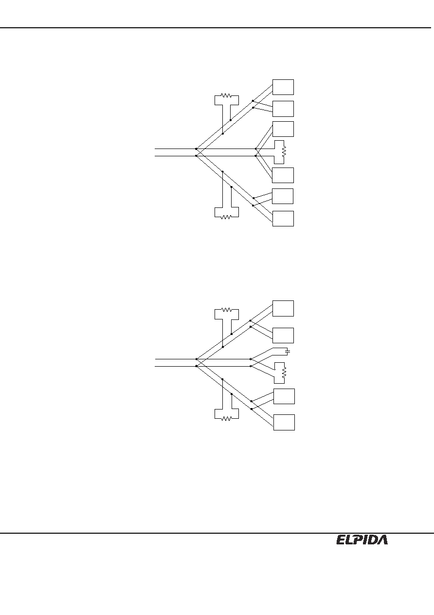
Logical Clock Net Structure
R = 200
R = 200
R = 200
DRAM
6DRAM loads (CK1 and /CK1, CK2 and /CK2)
DIMM
connector
DRAM
DRAM
R = 200
R = 200
R = 200
DRAM
4DRAM loads (CK0 and /CK0)
DIMM
connector
C2
DRAM
*C2: 2pF
DRAM
DRAM
DRAM
DRAM
DRAM
EBE11UD8AEFA-6
Data Sheet E0721E10 (Ver. 1.0)
10
Electrical Specifications
∑
All voltages are referenced to VSS (GND).
Absolute Maximum Ratings
Parameter Symbol
Value
Unit
Note
Voltage on any pin relative to VSS
VT
≠0.5 to +2.3
V
1
Supply voltage relative to VSS
VDD
≠0.5 to +2.3
V
Short circuit output current
IOS
50
mA
1
Power dissipation
PD
8
W
Operating case temperature
TC
0 to +95
∞C
1, 2
Storage temperature
Tstg
≠55 to +100
∞C
1
Note: 1. DDR2 SDRAM component specification.
2.
Supporting
0
∞
C to +85∞C and being able to extend to +95∞C with doubling auto-refresh commands in
frequency to a 32ms period (tREFI = 3.9
µ
s) and higher temperature self-refresh entry via the control of
EMRS (2) bit A7 is required.
Caution Exposing the device to stress above those listed in Absolute Maximum Ratings could cause
permanent damage. The device is not meant to be operated under conditions outside the limits
described in the operational section of this specification Exposure to Absolute Maximum Rating
conditions for extended periods may affect device reliability.
DC Operating Conditions (TC = 0∞C to +85∞C) (DDR2 SDRAM Component Specification)
Parameter Symbol
min.
typ.
max.
Unit
Notes
Supply voltage
VDD, VDDQ
1.7
1.8
1.9
V
4
VSS
0
0
0
V
VDDSPD
1.7
--
3.6
V
Input reference voltage
VREF
0.49
◊
VDDQ
0.50
◊
VDDQ 0.51
◊
VDDQ
V
1, 2
Termination voltage
VTT
VREF
-
0.04
VREF
VREF + 0.04
V
3
DC input logic high
VIH (DC)
VREF + 0.125
VDDQ + 0.3V
V
DC input low
VIL (DC)
-
0.3
VREF ≠ 0.125
V
AC input logic high
VIH (AC)
VREF + 0.200
V
AC input low
VIL (AC)
VREF
-
0.200
V
Notes: 1. The value of VREF may be selected by the user to provide optimum noise margin in the system. Typically
the value of VREF is expected to be about 0.5
◊
VDDQ of the transmitting device and VREF are expected
to track variations in VDDQ.
2. Peak to peak AC noise on VREF may not exceed
±
2% VREF (DC).
3. VTT of transmitting device must track VREF of receiving device.
4. VDDQ must be equal to VDD.

EBE11UD8AEFA-6
Data Sheet E0721E10 (Ver. 1.0)
11
DC Characteristics 1 (TC = 0∞C to +85∞C, VDD = 1.8V ± 0.1V, VSS = 0V)
Parameter Symbol
Grade
max.
Unit
Test
condition
Operating current
(ACT-PRE)
(Another rank is in IDD2P)
IDD0
1000 mA
Operating current
(ACT-PRE)
(Another rank is in IDD3N)
IDD0
1480 mA
one bank; tCK = tCK (IDD), tRC = tRC (IDD),
tRAS = tRAS min.(IDD);
CKE is H, /CS is H between valid commands;
Address bus inputs are SWITCHING;
Data bus inputs are SWITCHING
Operating current
(ACT-READ-PRE)
(Another rank is in IDD2P)
IDD1
1120 mA
Operating current
(ACT-READ-PRE)
(Another rank is in IDD3N)
IDD1
1600 mA
one bank; IOUT = 0mA;
BL = 4, CL = CL(IDD), AL = 0;
tCK = tCK (IDD), tRC = tRC (IDD),
tRAS = tRAS min.(IDD); tRCD = tRCD (IDD);
CKE is H, /CS is H between valid commands;
Address bus inputs are SWITCHING;
Data pattern is same as IDD4W
Precharge power-down
standby current
IDD2P
160 mA
all banks idle;
tCK = tCK (IDD);
CKE is L;
Other control and address bus inputs are STABLE;
Data bus inputs are FLOATING
Precharge quiet standby
current
IDD2Q
400 mA
all banks idle;
tCK = tCK (IDD);
CKE is H, /CS is H;
Other control and address bus inputs are STABLE;
Data bus inputs are FLOATING
Idle standby current
IDD2N
560 mA
all banks idle;
tCK = tCK (IDD);
CKE is H, /CS is H;
Other control and address bus inputs are SWITCHING;
Data bus inputs are SWITCHING
IDD3P-F
640 mA
Fast PDN Exit
MRS(12) = 0
Active power-down
standby current
IDD3P-S
400 mA
all banks open;
tCK = tCK (IDD);
CKE is L;
Other control and address bus
inputs are STABLE;
Data bus inputs are FLOATING
Slow PDN Exit
MRS(12) = 1
Active standby current
IDD3N
1120 mA
all banks open;
tCK = tCK (IDD), tRAS = tRAS max.(IDD), tRP = tRP (IDD);
CKE is H, /CS is H between valid commands;
Other control and address bus inputs are SWITCHING;
Data bus inputs are SWITCHING
Operating current
(Burst read operating)
(Another rank is in IDD2P)
IDD4R
1920
mA
Operating current
(Burst read operating)
(Another rank is in IDD3N)
IDD4R
2400
mA
all banks open, continuous burst reads, IOUT = 0mA;
BL = 4, CL = CL(IDD), AL = 0;
tCK = tCK (IDD), tRAS = tRAS max.(IDD), tRP = tRP (IDD);
CKE is H, /CS is H between valid commands;
Address bus inputs are SWITCHING;
Data pattern is same as IDD4W
Operating current
(Burst write operating)
(Another rank is in IDD2P)
IDD4W
1840
mA
Operating current
(Burst write operating)
(Another rank is in IDD3N)
IDD4W
2320
mA
all banks open, continuous burst writes;
BL = 4, CL = CL(IDD), AL = 0;
tCK = tCK (IDD), tRAS = tRAS max.(IDD), tRP = tRP (IDD);
CKE is H, /CS is H between valid commands;
Address bus inputs are SWITCHING;
Data bus inputs are SWITCHING
Auto-refresh current
(Another rank is in IDD2P)
IDD5
2240 mA
Auto-refresh current
(Another rank is in IDD3N)
IDD5
2720 mA
tCK = tCK (IDD);
Refresh command at every tRFC (IDD) interval;
CKE is H, /CS is H between valid commands;
Other control and address bus inputs are SWITCHING;
Data bus inputs are SWITCHING
EBE11UD8AEFA-6
Data Sheet E0721E10 (Ver. 1.0)
12
Parameter Symbol
Grade
max.
Unit
Test
condition
Self-refresh current
IDD6
96 mA
Self Refresh Mode;
CK and /CK at 0V;
CKE
0.2V;
Other control and address bus inputs are FLOATING;
Data bus inputs are FLOATING
Operating current
(Bank interleaving)
(Another rank is in IDD2P)
IDD7
2640 mA
Operating current
(Bank interleaving)
(Another rank is in IDD3N)
IDD7
3120 mA
all bank interleaving reads, IOUT = 0mA;
BL = 4, CL = CL(IDD), AL = tRCD (IDD)
-
1
◊
tCK (IDD);
tCK = tCK (IDD), tRC = tRC (IDD), tRRD = tRRD(IDD),
tRCD = 1
◊
tCK (IDD);
CKE is H, CS is H between valid commands;
Address bus inputs are STABLE during DESELECTs;
Data pattern is same as IDD4W;
Notes: 1. IDD specifications are tested after the device is properly initialized.
2. Input slew rate is specified by AC Input Test Condition.
3. IDD parameters are specified with ODT disabled.
4. Data bus consists of DQ, DM, DQS, /DQS, RDQS, /RDQS, LDQS, /LDQS, UDQS, and /UDQS. IDD
values must be met with all combinations of EMRS bits 10 and 11.
5. Definitions for IDD
L is defined as VIN
VIL (AC) (max.)
H is defined as VIN
VIH (AC) (min.)
STABLE is defined as inputs stable at an H or L level
FLOATING is defined as inputs at VREF = VDDQ/2
SWITCHING is defined as:
inputs changing between H and L every other clock cycle (once per two clocks) for address and control
signals, and inputs changing between H and L every other data transfer (once per clock) for DQ signals
not including masks or strobes.
6. Refer to AC Timing for IDD Test Conditions.
AC Timing for IDD Test Conditions
For purposes of IDD testing, the following parameters are to be utilized.
DDR2-667
Parameter 5-5-5
Unit
CL (IDD)
5
tCK
tRCD (IDD)
15
ns
tRC (IDD)
60
ns
tRRD (IDD)
7.5
ns
tCK (IDD)
3
ns
tRAS (min.)(IDD)
45
ns
tRAS (max.)(IDD)
70000
ns
tRP (IDD)
15
ns
tRFC (IDD)
105
ns
EBE11UD8AEFA-6
Data Sheet E0721E10 (Ver. 1.0)
13
DC Characteristics 2 (TC = 0∞C to +85∞C, VDD, VDDQ = 1.8V ± 0.1V)
(DDR2 SDRAM Component Specification)
Parameter Symbol
Value
Unit
Notes
Input leakage current
ILI
2
µ
A VDD
VIN
VSS
Output leakage current
ILO
5
µ
A VDDQ
VOUT
VSS
Minimum required output pull-up under AC
test load
VOH
VTT + 0.603
V
5
Maximum required output pull-down under
AC test load
VOL
VTT ≠ 0.603
V
5
Output timing measurement reference level VOTR
0.5
◊
VDDQ
V
1
Output minimum sink DC current
IOL
+13.4
mA
3, 4, 5
Output minimum source DC current
IOH
≠13.4
mA
2, 4, 5
Notes: 1. The VDDQ of the device under test is referenced.
2. VDDQ = 1.7V; VOUT = 1.42V.
3. VDDQ = 1.7V; VOUT = 0.28V.
4. The DC value of VREF applied to the receiving device is expected to be set to VTT.
5. After OCD calibration to 18
at TA = 25
∞
C, VDD = VDDQ = 1.8V.
DC Characteristics 3 (TC = 0∞C to +85
∞
C, VDD, VDDQ = 1.8V
±
0.1V)
(DDR2 SDRAM Component Specification)
Parameter Symbol
min.
max.
Unit
Notes
AC differential input voltage
VID (AC)
0.5
VDDQ
+
0.6
V
1, 2
AC differential cross point voltage
VIX (AC)
0.5
◊
VDDQ
-
0.175
0.5
◊
VDDQ
+
0.175
V
2
AC differential cross point voltage
VOX (AC)
0.5
◊
VDDQ
-
0.125
0.5
◊
VDDQ
+
0.125
V
3
Notes: 1. VID(AC) specifies the input differential voltage |VTR -VCP| required for switching, where VTR is the true
input signal (such as CK, DQS, LDQS or UDQS) and VCP is the complementary input signal (such as
/CK, /DQS, /LDQS or /UDQS). The minimum value is equal to VIH(AC)
-
VIL(AC).
2. The typical value of VIX(AC) is expected to be about 0.5
◊
VDDQ of the transmitting device and VIX(AC)
is expected to track variations in VDDQ . VIX(AC) indicates the voltage at which differential input signals
must cross.
3. The typical value of VOX(AC) is expected to be about 0.5
◊
VDDQ of the transmitting device and
VOX(AC) is expected to track variations in VDDQ . VOX(AC) indicates the voltage at which differential
output signals must cross.
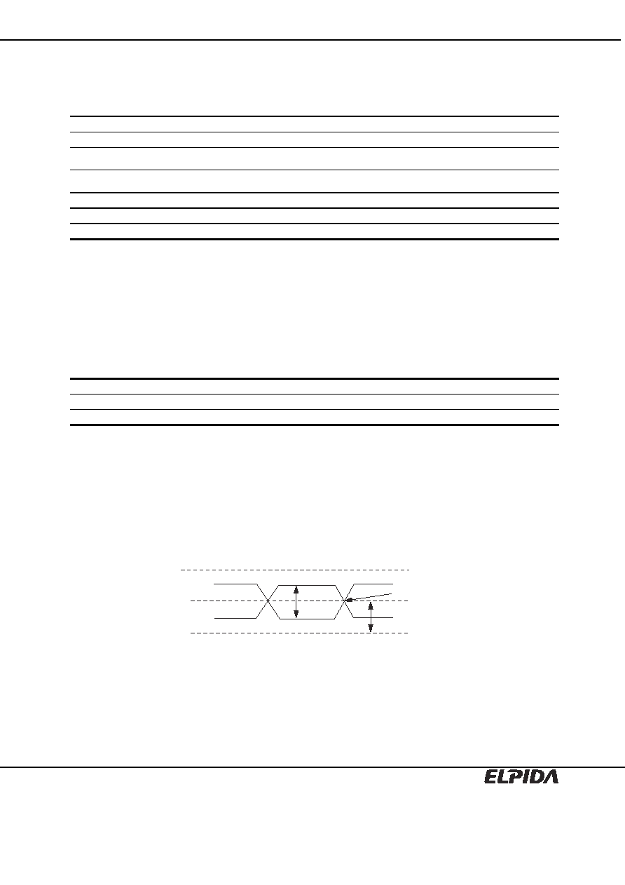
Crossing point
VSSQ
VTR
VCP
VID
VIX or VOX
VDDQ
Differential Signal Levels*
1, 2
EBE11UD8AEFA-6
Data Sheet E0721E10 (Ver. 1.0)
14
ODT DC Electrical Characteristics (TC = 0∞C to +85
∞
C, VDD, VDDQ = 1.8V
±
0.1V)
(DDR2 SDRAM Component Specification)
Parameter Symbol
min.
typ.
max.
Unit
Note
Rtt effective impedance value for EMRS (A6, A2)
=
0, 1
;
75
Rtt1(eff)
60 75 90
1
Rtt effective impedance value for EMRS (A6, A2)
=
1, 0
;
150
Rtt2(eff)
120 150 180
1
Rtt effective impedance value for EMRS (A6, A2)
=
1, 1
;
50
Rtt3(eff)
40 50 60
1
Deviation of VM with respect to VDDQ/2
VM
-
6
+
6
%
1
Note: 1. Test condition for Rtt measurements.
Measurement Definition for Rtt(eff)
Apply VIH (AC) and VIL (AC) to test pin separately, then measure current I(VIH(AC)) and I(VIL(AC)) respectively.
VIH(AC), and VDDQ values defined in SSTL
_
18.
VIH(AC)
-
VIL(AC)
I(VIH(AC))
-
I(VIL(AC))
Rtt(eff) =
Measurement Definition for
VM
Measure voltage (VM) at test pin (midpoint) with no load.
2
◊
VM
VDDQ
VM =
◊
100%
-
1
OCD Default Characteristics (TC = 0∞C to +85
∞
C, VDD, VDDQ = 1.8V
±
0.1V)
(DDR2 SDRAM Component Specification)
Parameter min.
typ.
max.
Unit
Notes
Output impedance
12.6
18
23.4
1
Pull-up and pull-down mismatch
0
4
1, 2
Output slew rate
1.5
5 V/ns
3,
4
Notes: 1. Impedance measurement condition for output source DC current: VDDQ = 1.7V; VOUT = 1420mV;
(VOUT
-
VDDQ)/IOH must be less than 23.4
for values of VOUT between VDDQ and VDDQ
-
280mV.
Impedance measurement condition for output sink DC current: VDDQ = 1.7V; VOUT = 280mV;
VOUT/IOL must be less than 23.4
for values of VOUT between 0V and 280mV.
2. Mismatch is absolute value between pull up and pull down, both are measured at same temperature and
voltage.
3. Slew rate measured from VIL(AC) to VIH(AC).
4. The absolute value of the slew rate as measured from DC to DC is equal to or greater than the slew rate
as measured from AC to AC. This is guaranteed by design and characterization.
EBE11UD8AEFA-6
Data Sheet E0721E10 (Ver. 1.0)
15
Pin Capacitance (TA = 25∞C, VDD = 1.8V ± 0.1V)
(DDR2 SDRAM Component Specification)
Parameter Symbol
Pins
min.
max.
Unit
Notes
CLK input pin capacitance
CCK
CK, /CK
1.0
2.0
pF
1
Input pin capacitance
CIN
/RAS, /CAS,
/WE, /CS,
CKE, ODT,
Address
1.0 2.0 pF 1
Input/output pin capacitance
CI/O
DQ, DQS, /DQS,
RDQS, /RDQS, DM
2.5 3.5 pF 2
Notes: 1. Matching within 0.25pF.
2.
Matching
within
0.50pF.
AC Characteristics (TC = 0∞C to +85
∞
C, VDD, VDDQ = 1.8V ± 0.1V, VSS = 0V)
(DDR2 SDRAM Component Specification)
-6E
Frequency (Mbps)
667
Parameter Symbol
min.
max.
Unit
Notes
/CAS latency
CL
5
5
tCK
Active to read or write command delay
tRCD
15
ns
Precharge command period
tRP
15
ns
Active to active/auto refresh command time
tRC
60
ns
DQ output access time from CK, /CK
tAC
-
450
+450
ps
DQS output access time from CK, /CK
tDQSCK
-
400
+400
ps
CK high-level width
tCH
0.45
0.55
tCK
CK low-level width
tCL
0.45
0.55
tCK
CK half period
tHP
min.
(tCL, tCH)
ps
Clock cycle time
tCK
3000
8000
ps
DQ and DM input hold time
tDH
175
ps
5
DQ and DM input setup time
tDS
100
ps
4
Control and Address input pulse width for each input tIPW
0.6
tCK
DQ and DM input pulse width for each input
tDIPW
0.35
tCK
Data-out high-impedance time from CK,/CK
tHZ
tAC max.
ps
Data-out low-impedance time from CK,/CK
tLZ
tAC min.
tAC max.
ps
DQS-DQ skew for DQS and associated DQ signals
tDQSQ
240
ps
DQ hold skew factor
tQHS
340
ps
DQ/DQS output hold time from DQS
tQH
tHP ≠ tQHS
ps
Write command to first DQS latching transition
tDQSS
WL
-
0.25
WL + 0.25
tCK
DQS input high pulse width
tDQSH
0.35
tCK
DQS input low pulse width
tDQSL
0.35
tCK
DQS falling edge to CK setup time
tDSS
0.2
tCK
DQS falling edge hold time from CK
tDSH
0.2
tCK
Mode register set command cycle time
tMRD
2
tCK
Write postamble
tWPST
0.4
0.6
tCK
EBE11UD8AEFA-6
Data Sheet E0721E10 (Ver. 1.0)
16
-6E
Frequency (Mbps)
667
Parameter Symbol
min.
max.
Unit
Notes
Write preamble
tWPRE
0.35
tCK
Address and control input hold time
tIH
275
ps
5
Address and control input setup time
tIS
200
ps
4
Read preamble
tRPRE
0.9
1.1
tCK
Read postamble
tRPST
0.4
0.6
tCK
Active to precharge command
tRAS
45
70000
ns
Active to auto-precharge delay
tRAP
tRCD min.
ns
Active bank A to active bank B command period
tRRD
7.5
ns
Write recovery time
tWR
15
ns
Auto precharge write recovery + precharge time
tDAL
(tWR/tCK)+
(tRP/tCK)
tCK 1
Internal write to read command delay
tWTR
7.5
ns
Internal read to precharge command delay
tRTP
7.5
ns
Exit self refresh to a non-read command
tXSNR
tRFC + 10
ns
Exit self refresh to a read command
tXSRD
200
tCK
Exit precharge power down to any non-read
command
tXP 2
tCK
Exit active power down to read command
tXARD
2
tCK 3
Exit active power down to read command
(slow exit/low power mode)
tXARDS 7
-
AL
tCK 2,
3
CKE minimum pulse width (high and low pulse width) tCKE
3
tCK
Output impedance test driver delay
tOIT
0
12
ns
Auto refresh to active/auto refresh command time
tRFC
105
ns
Average periodic refresh interval
(0
∞
C
TC
+85
∞
C)
tREFI
7.8
µ
s
(+85
∞
C
<
TC
+95
∞
C) tREFI
3.9
µ
s
Minimum time clocks remains ON after CKE
asynchronously drops low
tDELAY
tIS + tCK + tIH
ns
Notes: 1. For each of the terms above, if not already an integer, round to the next higher integer.
2. AL: Additive Latency.
3. MRS A12 bit defines which active power down exit timing to be applied.
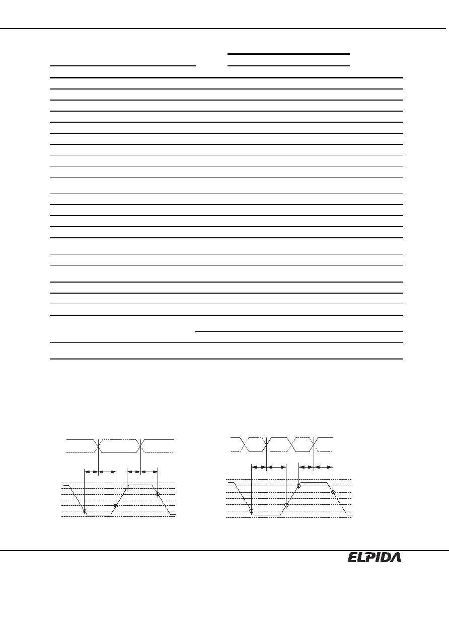
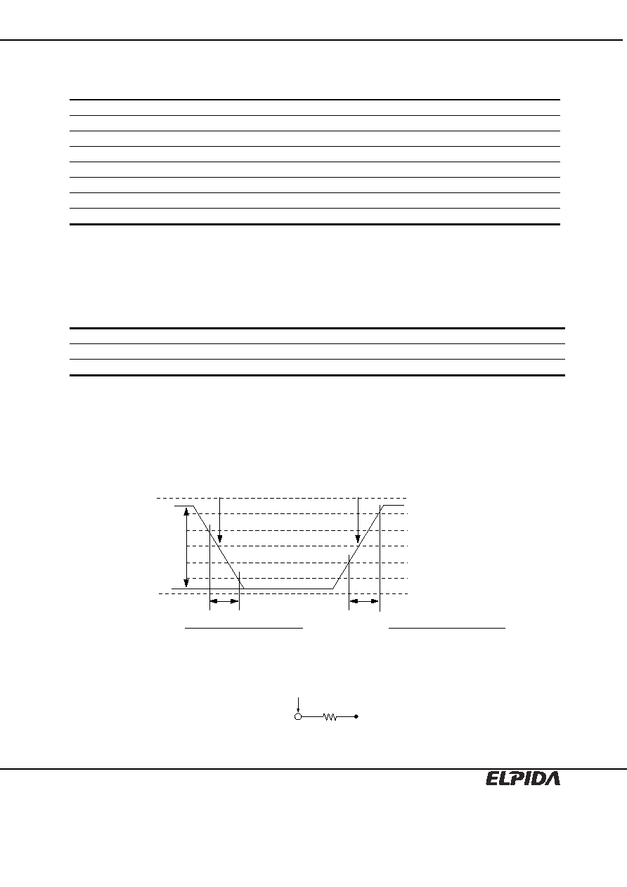
4. The figures of Input Waveform Timing 1 and 2 are referenced from the input signal crossing at the
VIH(AC) level for a rising signal and VIL(AC) for a falling signal applied to the device under test.
5. The figures of Input Waveform Timing 1 and 2 are referenced from the input signal crossing at the
VIH(DC) level for a rising signal and VIL(DC) for a falling signal applied to the device under test.
DQS
/DQS
tDS
tDH
tDS
tDH
VDDQ
VIH (AC)(min.)
VIH (DC)(min.)
VIL (DC)(max.)
VIL (AC)(max.)
VSS
VREF
CK
/CK
tIS
tIH
tIS
tIH
VDDQ
VIH (AC)(min.)
VIH (DC)(min.)
VIL (DC)(max.)
VIL (AC)(max.)
VSS
VREF
Input Waveform Timing 1 (tDS, tDH)
Input Waveform Timing 2 (tIS, tIH)
EBE11UD8AEFA-6
Data Sheet E0721E10 (Ver. 1.0)
17
ODT AC Electrical Characteristics (DDR2 SDRAM Component Specification)
Parameter Symbol
min.
max.
Unit
Notes
ODT turn-on delay
tAOND
2
2
tCK
ODT turn-on
tAON
tAC(min)
tAC(max)
+
700
ps
1
ODT turn-on (power down mode)
tAONPD
tAC(min)
+
2000
2tCK
+
tAC(max)
+
1000
ps
ODT turn-off delay
tAOFD
2.5
2.5
tCK
ODT turn-off
tAOF
tAC(min)
tAC(max)
+
600
ps
2
ODT turn-off (power down mode)
tAOFPD
tAC(min)
+
2000
2.5tCK
+
tAC(max)
+
1000
ps
ODT to power down entry latency
tANPD
3
3
tCK
ODT power down exit latency
tAXPD
8
8
tCK
Notes: 1. ODT turn on time min is when the device leaves high impedance and ODT resistance begins to turn on.
ODT turn on time max is when the ODT resistance is fully on. Both are measured from tAOND.
2. ODT turn off time min is when the device starts to turn off ODT resistance.
ODT turn off time max is when the bus is in high impedance. Both are measured from tAOFD.
AC Input Test Conditions
Parameter
Symbol
Value
Unit
Notes
Input reference voltage
VREF
0.5
◊
VDDQ
V
1
Input signal maximum peak to peak swing
VSWING(max.)
1.0
V
1
Input signal maximum slew rate
SLEW
1.0
V/ns
2, 3
Notes: 1. Input waveform timing is referenced to the input signal crossing through the VREF level applied to the
device under test.
2. The input signal minimum slew rate is to be maintained over the range from VIL(DC) (max.) to VIH(AC)
(min.) for rising edges and the range from VIH(DC) (min.) to VIL(AC) (max.) for falling edges as shown in
the below figure.
3. AC timings are referenced with input waveforms switching from VIL(AC) to VIH(AC) on the positive
transitions and VIH(AC) to VIL(AC) on the negative transitions.
VSWING(max.)
TR
TF
Start of falling edge input timing
Start of rising edge input timing
VIH (DC)(min.)
-
VIL (AC)(max.)
TF
Falling slew =
VDDQ
VIH (AC)(min.)
VIH (DC)(min.)
VIL (DC)(max.)
VIL (AC)(max.)
VSS
VREF
VIH (AC) min.
-
VIL (DC)(max.)
TR
Rising slew =
AC Input Test Signal Wave forms
VTT
Measurement point
DQ
RT =25
Output Load
EBE11UD8AEFA-6
Data Sheet E0721E10 (Ver. 1.0)
18
Pin Functions
CK, /CK (input pin)
The CK and the /CK are the master clock inputs. All inputs except DMs, DQSs and DQs are referred to the cross
point of the CK rising edge and the VREF level. When a read operation, DQSs and DQs are referred to the cross
point of the CK and the /CK. When a write operation, DMs and DQs are referred to the cross point of the DQS and
the VREF level. DQSs for write operation are referred to the cross point of the CK and the /CK.
/CS (input pin)
When /CS is low, commands and data can be input. When /CS is high, all inputs are ignored. However, internal
operations (bank active, burst operations, etc.) are held.
/RAS, /CAS, and /WE (input pins)
These pins define operating commands (read, write, etc.) depending on the combinations of their voltage levels.
See "Command operation".
A0 to A13 (input pins)
Row address (AX0 to AX13) is determined by the A0 to the A13 level at the cross point of the CK rising edge and the
VREF level in a bank active command cycle. Column address (AY0 to AY9) is loaded via the A0 to the A9 at the
cross point of the CK rising edge and the VREF level in a read or a write command cycle. This column address
becomes the starting address of a burst operation.
A10 (AP) (input pin)
A10 defines the precharge mode when a precharge command, a read command or a write command is issued. If
A10 = high when a precharge command is issued, all banks are precharged. If A10 = low when a precharge
command is issued, only the bank that is selected by BA1, BA0 is precharged. If A10 = high when read or write
command, auto-precharge function is enabled. While A10 = low, auto-precharge function is disabled.
BA0 and BA1 (input pins)
BA0, BA1 are bank select signals (BA). The memory array is divided into bank 0, bank 1, bank 2 and bank 3. (See
Bank Select Signal Table)
[Bank Select Signal Table]
BA0
BA1
Bank 0
L
L
Bank 1
H
L
Bank 2
L
H
Bank 3
H
H
Remark: H: VIH. L: VIL.
CKE (input pin)
CKE controls power down and self-refresh. The power down and the self-refresh commands are entered when the
CKE is driven low and exited when it resumes to high.
The CKE level must be kept for 1 CK cycle at least, that is, if CKE changes at the cross point of the CK rising edge
and the VREF level with proper setup time tIS, at the next CK rising edge CKE level must be kept with proper hold
time tIH.
DQ (input and output pins)
Data are input to and output from these pins.
DQS and /DQS (input and output pin)
DQS and /DQS provide the read data strobes (as output) and the write data strobes (as input).
EBE11UD8AEFA-6
Data Sheet E0721E10 (Ver. 1.0)
19
DM (input pins)
DM is the reference signal of the data input mask function. DMs are sampled at the cross point of DQS and /DQS.
VDD (power supply pins)
1.8V is applied. (VDD is for the internal circuit.)
VDDSPD (power supply pin)
1.8V is applied (For serial EEPROM).
VSS (power supply pin)
Ground is connected.
Detailed Operation Part and Timing Waveforms
Refer to the EDE5104AESK, EDE5108AESK datasheet (E0562E).
EBE11UD8AEFA-6
Data Sheet E0721E10 (Ver. 1.0)
20
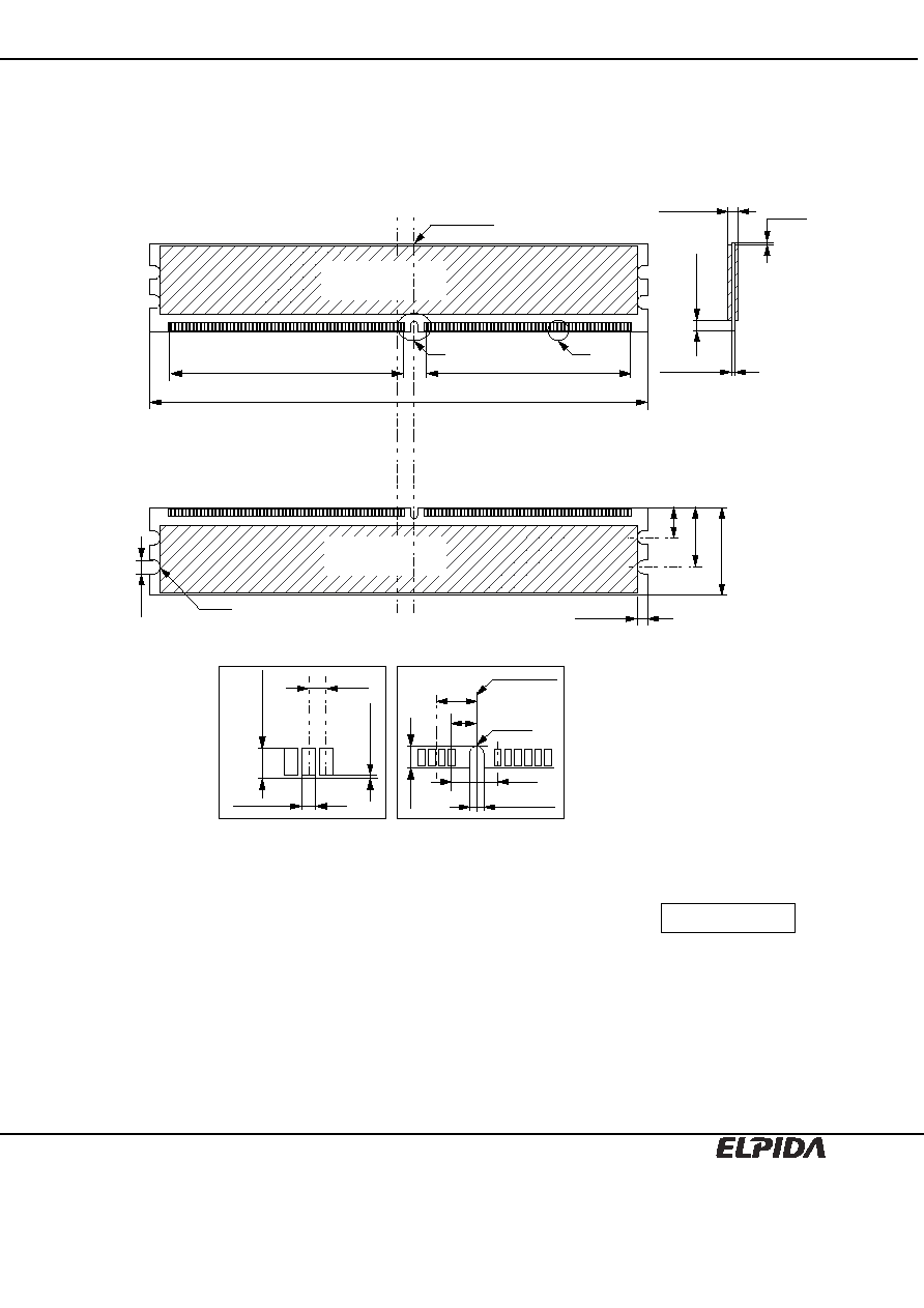
Physical Outline
Detail A
0.20 ± 0.15
2.50 ± 0.20
1.00
133.35
(DATUM -A-)
63.00
55.00
A
B
1
120
240
121
FULL R
0.80 ± 0.05
Unit: mm
1.27 ± 0.10
3.00
4.00 min
10.00
4.00
17.80
30.00
4.00 max
0.5 min
Component area
(Front)
Component area
(Back)
5.00
Detail B
3.80
1.50 ± 0.10
2.50
4.00
FULL R
(DATUM -A-)
ECA-TS2-0093-01
EBE11UD8AEFA-6
Data Sheet E0721E10 (Ver. 1.0)
21
CAUTION FOR HANDLING MEMORY MODULES
When handling or inserting memory modules, be sure not to touch any components on the modules, such as
the memory ICs, chip capacitors and chip resistors. It is necessary to avoid undue mechanical stress on
these components to prevent damaging them.
In particular, do not push module cover or drop the modules in order to protect from mechanical defects,
which would be electrical defects.
When re-packing memory modules, be sure the modules are not touching each other.
Modules in contact with other modules may cause excessive mechanical stress, which may damage the
modules.
MDE0202
NOTES FOR CMOS DEVICES
1
PRECAUTION AGAINST ESD FOR MOS DEVICES
Exposing the MOS devices to a strong electric field can cause destruction of the gate
oxide and ultimately degrade the MOS devices operation. Steps must be taken to stop
generation of static electricity as much as possible, and quickly dissipate it, when once
it has occurred. Environmental control must be adequate. When it is dry, humidifier
should be used. It is recommended to avoid using insulators that easily build static
electricity. MOS devices must be stored and transported in an anti-static container,
static shielding bag or conductive material. All test and measurement tools including
work bench and floor should be grounded. The operator should be grounded using
wrist strap. MOS devices must not be touched with bare hands. Similar precautions
need to be taken for PW boards with semiconductor MOS devices on it.
2
HANDLING OF UNUSED INPUT PINS FOR CMOS DEVICES
No connection for CMOS devices input pins can be a cause of malfunction. If no
connection is provided to the input pins, it is possible that an internal input level may be
generated due to noise, etc., hence causing malfunction. CMOS devices behave
differently than Bipolar or NMOS devices. Input levels of CMOS devices must be fixed
high or low by using a pull-up or pull-down circuitry. Each unused pin should be connected
to V
DD
or GND with a resistor, if it is considered to have a possibility of being an output
pin. The unused pins must be handled in accordance with the related specifications.
3
STATUS BEFORE INITIALIZATION OF MOS DEVICES
Power-on does not necessarily define initial status of MOS devices. Production process
of MOS does not define the initial operation status of the device. Immediately after the
power source is turned ON, the MOS devices with reset function have not yet been
initialized. Hence, power-on does not guarantee output pin levels, I/O settings or
contents of registers. MOS devices are not initialized until the reset signal is received.
Reset operation must be executed immediately after power-on for MOS devices having
reset function.
CME0107
EBE11UD8AEFA-6
Data Sheet E0721E10 (Ver. 1.0)
22
µ
BGA is a registered trademark of Tessera, Inc.
All other trademarks are the intellectual property of their respective owners.
M01E0107
No part of this document may be copied or reproduced in any form or by any means without the prior
written consent of Elpida Memory, Inc.
Elpida Memory, Inc. does not assume any liability for infringement of any intellectual property rights
(including but not limited to patents, copyrights, and circuit layout licenses) of Elpida Memory, Inc. or
third parties by or arising from the use of the products or information listed in this document. No license,
express, implied or otherwise, is granted under any patents, copyrights or other intellectual property
rights of Elpida Memory, Inc. or others.
Descriptions of circuits, software and other related information in this document are provided for
illustrative purposes in semiconductor product operation and application examples. The incorporation of
these circuits, software and information in the design of the customer's equipment shall be done under
the full responsibility of the customer. Elpida Memory, Inc. assumes no responsibility for any losses
incurred by customers or third parties arising from the use of these circuits, software and information.
[Product applications]
Elpida Memory, Inc. makes every attempt to ensure that its products are of high quality and reliability.
However, users are instructed to contact Elpida Memory's sales office before using the product in
aerospace, aeronautics, nuclear power, combustion control, transportation, traffic, safety equipment,
medical equipment for life support, or other such application in which especially high quality and
reliability is demanded or where its failure or malfunction may directly threaten human life or cause risk
of bodily injury.
[Product usage]
Design your application so that the product is used within the ranges and conditions guaranteed by
Elpida Memory, Inc., including the maximum ratings, operating supply voltage range, heat radiation
characteristics, installation conditions and other related characteristics. Elpida Memory, Inc. bears no
responsibility for failure or damage when the product is used beyond the guaranteed ranges and
conditions. Even within the guaranteed ranges and conditions, consider normally foreseeable failure
rates or failure modes in semiconductor devices and employ systemic measures such as fail-safes, so
that the equipment incorporating Elpida Memory, Inc. products does not cause bodily injury, fire or other
consequential damage due to the operation of the Elpida Memory, Inc. product.
[Usage environment]
This product is not designed to be resistant to electromagnetic waves or radiation. This product must be
used in a non-condensing environment.
If you export the products or technology described in this document that are controlled by the Foreign
Exchange and Foreign Trade Law of Japan, you must follow the necessary procedures in accordance
with the relevant laws and regulations of Japan. Also, if you export products/technology controlled by
U.S. export control regulations, or another country's export control laws or regulations, you must follow
the necessary procedures in accordance with such laws or regulations.
If these products/technology are sold, leased, or transferred to a third party, or a third party is granted
license to use these products, that third party must be made aware that they are responsible for
compliance with the relevant laws and regulations.
The information in this document is subject to change without notice. Before using this document, confirm that this is the latest version.