Document Outline
- COVER
- Description
- Features
- Ordering Information
- Pin Configurations
- Pin Description
- Serial PD Matrix
- Block Diagram
- Logical Clock Net Structure
- Electrical Specifications
- Absolute Maximum Ratings
- DC Operating Conditions
- DC Characteristics 1
- AC Timing for IDD Test Conditions
- DC Characteristics 2
- DC Characteristics 3
- ODT DC Electrical Characteristics
- OCD Default Characteristics
- Pin Capacitance
- AC Characteristics
- ODT AC Electrical Characteristics
- Pin Functions
- Detailed Operation Part and Timing Waveforms
- Physical Outline
Document No. E0782E20 (Ver. 2.0)
Date Published October 2005 (K) Japan
Printed in Japan
URL: http://www.elpida.com
Elpida Memory, Inc. 2005
DATA SHEET
1GB Unbuffered DDR2 SDRAM DIMM
EBE11UD8AGFA (128M words
◊
64 bits, 2 Ranks)
Description
The EBE11UD8AGFA is 128M words
◊
64 bits, 2 ranks
DDR2 SDRAM unbuffered module, mounting 16 pieces
of 512M bits DDR2 SDRAM sealed in FBGA (
µ
BGA
)
package. Read and write operations are performed at
the cross points of the CK and the /CK. This high-
speed data transfer is realized by the 4 bits prefetch-
pipelined architecture. Data strobe (DQS and /DQS)
both for read and write are available for high speed and
reliable data bus design. By setting extended mode
register, the on-chip Delay Locked Loop (DLL) can be
set enable or disable. This module provides high
density mounting without utilizing surface mount
technology. Decoupling capacitors are mounted
beside each FBGA (
µ
BGA) on the module board.
Note: Do not push the components or drop the
modules in order to avoid mechanical defects,
which may result in electrical defects.
Features
∑
240-pin socket type dual in line memory module
(DIMM)
PCB height: 30.0mm
Lead pitch: 1.0mm
Lead-free (RoHS compliant)
∑
Power supply: VDD
=
1.8V
±
0.1V
∑
Data rate: 667Mbps/533Mbps/400Mbps (max.)
∑
SSTL_18 compatible I/O
∑
Double-data-rate architecture: two data transfers per
clock cycle
∑
Bi-directional, differential data strobe (DQS and
/DQS) is transmitted/received with data, to be used in
capturing data at the receiver
∑
DQS is edge aligned with data for READs: center-
aligned with data for WRITEs
∑
Differential clock inputs (CK and /CK)
∑
DLL aligns DQ and DQS transitions with CK
transitions
∑
Commands entered on each positive CK edge: data
and data mask referenced to both edges of DQS
∑
Four internal banks for concurrent operation
(components)
∑
Data mask (DM) for write data
∑
Burst lengths: 4, 8
∑
/CAS Latency (CL): 3, 4, 5
∑
Auto precharge operation for each burst access
∑
Auto refresh and self refresh modes
∑
Average refresh period
7.8
µ
s at 0
∞
C
TC
+
85
∞
C
3.9
µ
s at
+
85
∞
C
<
TC
+
95
∞
C
∑
Posted CAS by programmable additive latency for
better command and data bus efficiency
∑
Off-Chip-Driver Impedance Adjustment and On-Die-
Termination for better signal quality
∑
/DQS can be disabled for single-ended Data Strobe
operation
EBE11UD8AGFA
Data Sheet E0782E20 (Ver. 2.0)
2
Ordering Information
Part number
Data rate
Mbps (max.)
Component
JEDEC speed bin
(CL-tRCD-tRP)
Package
Contact
pad
Mounted devices
EBE11UD8AGFA-6E-E 667
DDR2-667 (5-5-5)
EDE5108AGSE-6E-E
EBE11UD8AGFA-5C-E 533
DDR2-533 (4-4-4)
EDE5108AGSE-6E-E
EDE5108AGSE-5C-E
EBE11UD8AGFA-4A-E 400
DDR2-400
(3-3-3)
240-pin DIMM
(lead-free)
Gold
EDE5108AGSE-6E-E
EDE5108AGSE-5C-E
EDE5108AGSE-4A-E
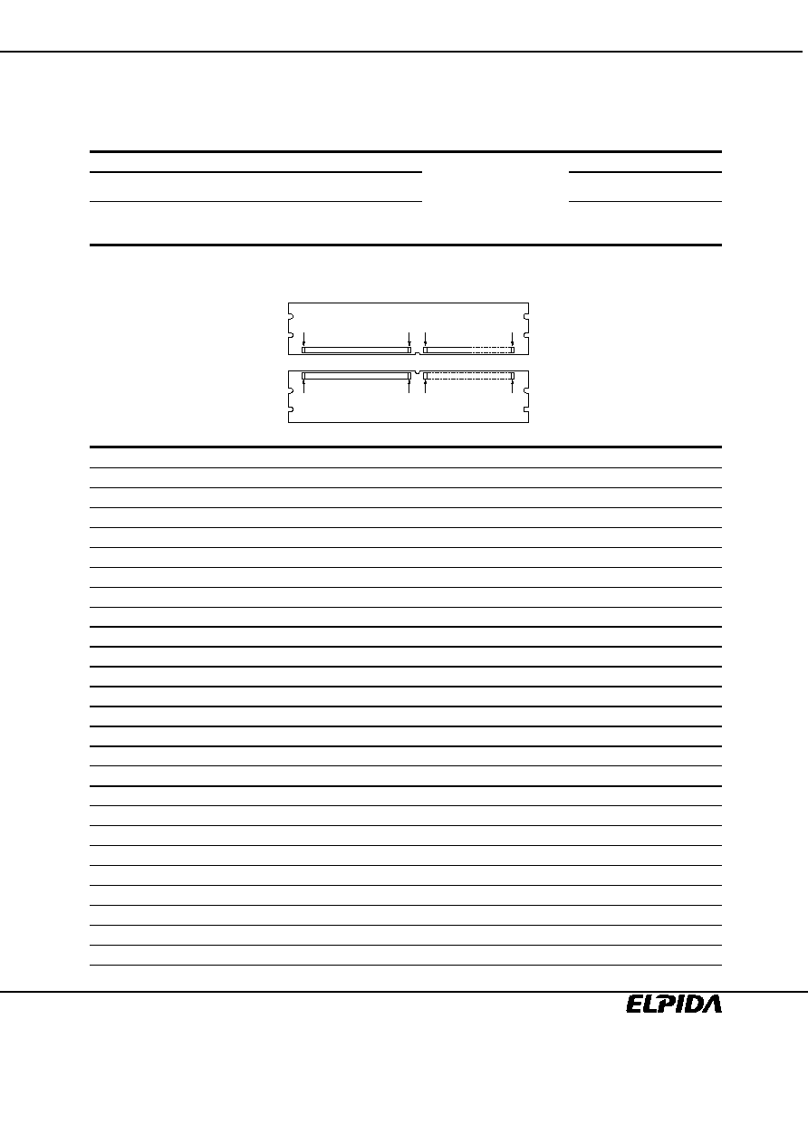
Pin Configurations
1 pin
Front side
Back side
64 pin 65 pin
120 pin
121 pin
184 pin 185 pin
240 pin
Pin No.
Pin name
Pin No.
Pin name
Pin No.
Pin name
Pin No.
Pin name
1 VREF
61 A4 121 VSS 181 VDD
2 VSS 62 VDD 122 DQ4 182 A3
3 DQ0 63 A2 123 DQ5 183 A1
4 DQ1 64 VDD 124 VSS 184 VDD
5 VSS 65 VSS 125 DM0 185 CK0
6 /DQS0
66 VSS 126 NC 186 /CK0
7 DQS0
67 VDD 127 VSS 187 VDD
8 VSS 68 NC 128 DQ6 188 A0
9 DQ2 69 VDD 129 DQ7 189 VDD
10 DQ3 70 A10/AP
130 VSS 190 BA1
11 VSS 71 BA0 131 DQ12 191 VDD
12 DQ8 72
VDD 132 DQ13 192 /RAS
13 DQ9 73 /WE 133 VSS 193 /CS0
14 VSS 74 /CAS 134 DM1 194 VDD
15 /DQS1
75 VDD 135 NC 195 ODT0
16 DQS1 76 /CS1 136 VSS 196 A13
17 VSS 77 ODT1 137 CK1 197 VDD
18 NC 78 VDD 138 /CK1 198 VSS
19 NC 79 VSS 139 VSS 199 DQ36
20 VSS 80
DQ32 140 DQ14 200 DQ37
21 DQ10 81
DQ33 141 DQ15 201 VSS
22 DQ11
82 VSS 142 VSS 202 DM4
23 VSS 83 /DQS4
143 DQ20 203 NC
24 DQ16 84 DQS4 144 DQ21 204 VSS
25 DQ17
85 VSS 145 VSS 205 DQ38
26 VSS 86 DQ34 146 DM2 206 DQ39
EBE11UD8AGFA
Data Sheet E0782E20 (Ver. 2.0)
3
Pin No.
Pin name
Pin No.
Pin name
Pin No.
Pin name
Pin No.
Pin name
27 /DQS2
87 DQ35 147 NC 207 VSS
28 DQS2
88 VSS 148 VSS 208 DQ44
29 VSS 89
DQ40 149 DQ22 209 DQ45
30 DQ18 90
DQ41 150 DQ23 210 VSS
31 DQ19
91 VSS 151 VSS 211 DM5
32 VSS 92 /DQS5
152 DQ28 212 NC
33 DQ24 93 DQS5 153 DQ29 213 VSS
34 DQ25
94 VSS 154 VSS 214 DQ46
35 VSS 95 DQ42 155 DM3 215 DQ47
36 /DQS3
96 DQ43 156 NC 216 VSS
37 DQS3
97 VSS 157 VSS 217 DQ52
38 VSS 98
DQ48 158 DQ30 218 DQ53
39 DQ26 99
DQ49 159 DQ31 219 VSS
40 DQ27
100 VSS 160 VSS 220 CK2
41 VSS 101 SA2 161 NC 221 /CK2
42
NC 102 NC 162 NC 222 VSS
43 NC 103 VSS 163 VSS 223 DM6
44 VSS 104 /DQS6
164 NC 224 NC
45 NC 105 DQS6 165 NC 225 VSS
46 NC 106 VSS
166 VSS 226 DQ54
47 VSS 107 DQ50 167 NC 227 DQ55
48 NC 108 DQ51 168 NC 228 VSS
49 NC 109 VSS 169 VSS 229 DQ60
50 VSS 110 DQ56 170 VDD 230 DQ61
51 VDD 111 DQ57 171 CKE1 231 VSS
52 CKE0 112 VSS 172 VDD 232 DM7
53 VDD 113 /DQS7
173 NC 233 NC
54 NC 114 DQS7 174 NC 234 VSS
55 NC 115 VSS 175 VDD 235 DQ62
56 VDD 116 DQ58 176 A12 236 DQ63
57 A11 117 DQ59 177 A9 237 VSS
58 A7 118 VSS 178 VDD 238 VDDSPD
59 VDD 119 SDA 179 A8 239 SA0
60 A5 120 SCL 180 A6 240 SA1
EBE11UD8AGFA
Data Sheet E0782E20 (Ver. 2.0)
4
Pin Description
Pin name
Function
A0 to A13
Address input
Row address
A0 to A13
Column address
A0 to A9
A10 (AP)
Auto precharge
BA0, BA1
Bank select address
DQ0 to DQ63
Data input/output
/RAS
Row address strobe command
/CAS
Column address strobe command
/WE Write
enable
/CS0, /CS1
Chip select
CKE0, CKE1
Clock enable
CK0 to CK2
Clock input
/CK0 to /CK2
Differential clock input
DQS0 to DQS7, /DQS0 to /DQS7
Input and output data strobe
DM0 to DM7
Input mask
SCL
Clock input for serial PD
SDA
Data input/output for serial PD
SA0 to SA2
Serial address input
VDD
Power for internal circuit
VDDSPD
Power for serial EEPROM
VREF
Input reference voltage
VSS Ground
ODT0, ODT1
ODT control
NC No
connection
EBE11UD8AGFA
Data Sheet E0782E20 (Ver. 2.0)
5
Serial PD Matrix
Byte No.
Function described
Bit7 Bit6 Bit5 Bit4 Bit3 Bit2 Bit1 Bit0 Hex
value Comments
0
Number of bytes utilized by module
manufacturer
1 0 0 0 0 0 0 0 80H 128
bytes
1
Total number of bytes in serial PD
device
0 0 0 0 1 0 0 0 08H 256
bytes
2
Memory
type
0 0 0 0 1 0 0 0 08H DDR2
SDRAM
3
Number
of
row
address
0 0 0 0 1 1 1 0 0EH 14
4
Number
of
column
address
0 0 0 0 1 0 1 0 0AH 10
5
Number
of
DIMM
ranks
0 1 1 0 0 0 0 1 61H 2
6
Module
data
width
0 1 0 0 0 0 0 0 40H 64
7
Module
data
width
continuation
0 0 0 0 0 0 0 0 00H 0
8
Voltage interface level of this assembly 0
0
0
0
0
1
0
1
05H
SSTL 1.8V
9
DDR SDRAM cycle time, CL = 5
-6E
0 0 1 1 0 0 0 0 30H 3.0ns*
1
-5C
0 0 1 1 1 1 0 1 3DH 3.75ns*
1
-4A
0 1 0 1 0 0 0 0 50H 5.0ns*
1
10
SDRAM access from clock (tAC)
-6E
0 1 0 0 0 1 0 1 45H 0.45ns*
1
-5C
0 1 0 1 0 0 0 0 50H 0.5ns*
1
-4A
0 1 1 0 0 0 0 0 60H 0.6ns*
1
11
DIMM
configuration
type
0 0 0 0 0 0 0 0 00H None.
12
Refresh
rate/type
1 0 0 0 0 0 1 0 82H 7.8
µ
s
13
Primary
SDRAM
width
0 0 0 0 1 0 0 0 08H
◊
8
14
Error
checking
SDRAM
width
0 0 0 0 0 0 0 0 00H None.
15
Reserved
0 0 0 0 0 0 0 0 00H 0
16
SDRAM device attributes:
Burst length supported
0 0 0 0 1 1 0 0 0CH 4,8
17
SDRAM device attributes: Number of
banks on SDRAM device
0 0 0 0 0 1 0 0 04H 4
18
SDRAM device attributes:
/CAS latency
0 0 1 1 1 0 0 0 38H 3,
4,
5
19
DIMM
Mechanical
Characteristics 0 0 0 0 0 0 0 1 01H 4.00mm
max.
20
DIMM
type
information
0 0 0 0 0 0 1 0 02H Unbuffered
21
SDRAM
module
attributes
0 0 0 0 0 0 0 0 00H Normal
22
SDRAM
device
attributes:
General 0 0 0 0 0 0 1 1 03H
Weak Driver 50
ODT Support
23
Minimum clock cycle time at CL = 4
-6E, -5C
0 0 1 1 1 1 0 1 3DH 3.75ns*
1
-4A
0 1 0 1 0 0 0 0 50H 5.0ns*
1
24
Maximum data access time (tAC) from
clock at CL = 4
-6E, -5C
0 1 0 1 0 0 0 0 50H 0.5ns*
1
-4A
0 1 1 0 0 0 0 0 60H 0.6ns*
1
25
Minimum clock cycle time at CL = 3
0
1
0
1
0
0
0
0
50H
5.0ns*
1
26
Maximum data access time (tAC) from
clock at CL = 3
0 1 1 0 0 0 0 0 60H 0.6ns*
1
27
Minimum row precharge time (tRP)
0
0
1
1
1
1
0
0
3CH
15ns