Document Outline
- COVER
- Description
- Features
- Ordering Information
- Module Pad Names
- Module Connector Pad Description
- Block Diagram
- Electrical Specifications
- Absolute Maximum Ratings
- DC Recommended Electrical Conditions
- AC Electrical Specifications
- Adjusted delta TPD Specification
- RIMM Module Current Profile
- Physical Outline

Document No. E0310E20 (Ver. 2.0)
Date Published April 2003 (K) Japan
URL: http://www.elpida.com
Elpida Memory, Inc. 2002-2003
DATA SHEET
256MB Direct Rambus
DRAM RIMM
Module
EBR25EC8ABFD (128M words
◊
◊
◊
◊
18 bits)
Description
The Direct Rambus RIMM module is a general-purpose
high-performance memory module subsystem suitable
for use in a broad range of applications including
computer memory, personal computers, workstations,
and other applications where high bandwidth and low
latency are required.
The EBR25EC8ABFD consists of 8 pieces of 288M
Direct Rambus DRAM (Direct RDRAM
) devices.
These are extremely high-speed CMOS DRAMs
organized as 16M words by 18 bits. The use of
Rambus Signaling Level (RSL) technology permits
1066MHz or 800MHz transfer rates while using
conventional system and board design technologies.
The architecture of the Direct RDRAM enables the
highest sustained bandwidth for multiple, simultaneous,
randomly addressed memory transactions.
The separate control and data buses with independent
row and column control yield over 95% bus efficiency.
The Direct RDRAM device's 32 banks support up to
four simultaneous transactions per device.
Features
∑
256MB Direct RDRAM storage and 256 banks total
on module
∑
High speed 1066MHz/800MHz Direct RDRAM
devices
∑
184 edge connector pads with 1mm pad spacing
Module PCB size: 133.35mm
◊
34.925mm
◊
1.27mm
Gold plated edge connector pads contacts
∑
Serial Presence Detect (SPD) support
∑
Operates from a 2.5V supply
∑
Low power and power down self refresh modes
∑
Separate Row and Column buses for higher
efficiency
∑
RDRAM
devices use Chip Scale Package (CSP)
FBGA (
µ
BGA
) package

EBR25EC8ABFD
Data Sheet E0310E20 (Ver. 2.0)
2
Ordering Information
Part number
Organization
I/O Freq.
(MHz)
RAS access
time (ns)
Package
Mounted devices
EBR25EC8ABFD-AEP
128M x 18
1066
32 (32P)
184 edge connector pads
RIMM with heat spreader
EDR2518ABSE
EBR25EC8ABFD-AE
32
Edge connector: Gold plated
EBR25EC8ABFD-AD
35
EBR25EC8ABFD-8C
800
40
Module Pad Names
Pad
Signal Name Pad
Signal Name
Pad
Signal Name Pad
Signal Name
A1
GND
B1
GND
A47
NC
B47
NC
A2
LDQA8
B2
LDQA7
A48
NC
B48
NC
A3
GND
B3
GND
A49
NC
B49
NC
A4
LDQA6
B4
LDQA5
A50
NC
B50
NC
A5
GND
B5
GND
A51
VREF
B51
VREF
A6
LDQA4
B6
LDQA3
A52
GND
B52
GND
A7
GND
B7
GND
A53
SCL
B53
SA0
A8
LDQA2
B8
LDQA1
A54
VDD
B54
VDD
A9
GND
B9
GND
A55
SDA
B55
SA1
A10
LDQA0
B10
LCFM
A56
SVDD
B56
SVDD
A11
GND
B11
GND
A57
SWP
B57
SA2
A12
LCTMN
B12
LCFMN
A58
VDD
B58
VDD
A13
GND
B13
GND
A59
RSCK
B59
RCMD
A14
LCTM
B14
NC
A60
GND
B60
GND
A15
GND
B15
GND
A61
RDQB7
B61
RDQB8
A16
NC
B16
LROW2
A62
GND
B62
GND
A17
GND
B17
GND
A63
RDQB5
B63
RDQB6
A18
LROW1
B18
LROW0
A64
GND
B64
GND
A19
GND
B19
GND
A65
RDQB3
B65
RDQB4
A20
LCOL4
B20
LCOL3
A66
GND
B66
GND
A21
GND
B21
GND
A67
RDQB1
B67
RDQB2
A22
LCOL2
B22
LCOL1
A68
GND
B68
GND
A23
GND
B23
GND
A69
RCOL0
B69
RDQB0
A24
LCOL0
B24
LDQB0
A70
GND
B70
GND
A25
GND
B25
GND
A71
RCOL2
B71
RCOL1
A26
LDQB1
B26
LDQB2
A72
GND
B72
GND
A27
GND
B27
GND
A73
RCOL4
B73
RCOL3
A28
LDQB3
B28
LDQB4
A74
GND
B74
GND
A29
GND
B29
GND
A75
RROW1
B75
RROW0
A30
LDQB5
B30
LDQB6
A76
GND
B76
GND
A31
GND
B31
GND
A77
NC
B77
RROW2
A32
LDQB7
B32
LDQB8
A78
GND
B78
GND
A33
GND
B33
GND
A79
RCTM
B79
NC
A34
LSCK
B34
LCMD
A80
GND
B80
GND

EBR25EC8ABFD
Data Sheet E0310E20 (Ver. 2.0)
3
Pad
Signal Name Pad
Signal Name
Pad
Signal Name Pad
Signal Name
A35
VCMOS
B35
VCMOS
A81
RCTMN
B81
RCFMN
A36
SOUT
B36
SIN
A82
GND
B82
GND
A37
VCMOS
B37
VCMOS
A83
RDQA0
B83
RCFM
A38
NC
B38
NC
A84
GND
B84
GND
A39
GND
B39
GND
A85
RDQA2
B85
RDQA1
A40
NC
B40
NC
A86
GND
B86
GND
A41
VDD
B41
VDD
A87
RDQA4
B87
RDQA3
A42
VDD
B42
VDD
A88
GND
B88
GND
A43
NC
B43
NC
A89
RDQA6
B89
RDQA5
A44
NC
B44
NC
A90
GND
B90
GND
A45
NC
B45
NC
A91
RDQA8
B91
RDQA7
A46
NC
B46
NC
A92
GND
B92
GND

EBR25EC8ABFD
Data Sheet E0310E20 (Ver. 2.0)
4
Module Connector Pad Description
Signal
Module
Connector Pads
I/O
Type
Description
GND
A1, A3, A5, A7, A9, A11,
A13, A15, A17, A19, A21,
A23, A25, A27, A29, A31,
A33, A39, A52, A60, A62,
A64, A66, A68, A70, A72,
A74, A76, A78, A80, A82,
A84, A86, A88, A90, A92,
B1, B3, B5, B7, B9, B11,
B13, B15, B17, B19, B21,
B23, B25, B27, B29, B31,
B33, B39, B52, B60, B62,
B64, B66, B68, B70, B72,
B74, B76, B78, B80, B82,
B84, B86, B88, B90, B92
--
--
Ground reference for RDRAM core and interface. 72
PCB connector pads.
LCFM
B10
I
RSL
Clock from master. Interface clock used for receiving
RSL signals from the Channel. Positive polarity.
LCFMN
B12
I
RSL
Clock from master. Interface clock used for receiving
RSL signals from the Channel. Negative polarity.
LCMD
B34
I
VCMOS
Serial Command used to read from and write to the
control registers. Also used for power management.
LCOL4..LCOL0
A20, B20, A22, B22, A24 I
RSL
Column bus. 5-bit bus containing control and address
information for column accesses.
LCTM
A14
I
RSL
Clock to master. Interface clock used for transmitting
RSL signals to the Channel. Positive polarity.
LCTMN
A12
I
RSL
Clock to master. Interface clock used for transmitting
RSL signals to the Channel. Negative polarity.
LDQA8..LDQA0
A2, B2,A4, B4, A6, B6, A8,
B8, A10
I/O
RSL
Data bus A. A 9-bit bus carrying a byte of read or write
data between the Channel and the RDRAM.
LDQB8..LDQB0
B32, A32, B30, A30, B28,
A28, B26, A26, B24
I/O
RSL
Data bus B. A 9-bit bus carrying a byte of read or write
data between the Channel and the RDRAM.
LROW2..LROW0 B16, A18, B18
I
RSL
Row bus. 3-bit bus containing control and address
information for row accesses.
LSCK
A34
I
VCMOS
Serial clock input. Clock source used to read from and
write to the RDRAM control registers.
NC
A16, B14, A38, B38, A40,
B40, A77, B79, A43, B43,
A44, B44, A45, B45, A46,
B46, A47, B47, A48, B48,
A49, B49, A50, B50
--
--
These pads are not connected. These 24 connector
pads are reserved for future use.
RCFM
B83
I
RSL
Clock from master. Interface clock used for receiving
RSL signals from the Channel. Positive polarity.
RCFMN
B81
I
RSL
Clock from master. Interface clock used for receiving
RSL signals from the Channel. Negative polarity.
RCMD
B59
I
VCMOS
Serial Command Input used to read from and write to
the control registers. Also used for power
management.
RCOL4..RCOL0
A73, B73, A71, B71, A69 I
RSL
Column bus. 5-bit bus containing control and address
information for column accesses.
RCTM
A79
I
RSL
Clock to master. Interface clock used for transmitting
RSL signals to the Channel. Positive polarity.
RCTMN
A81
I
RSL
Clock to master. Interface clock used for transmitting
RSL signals to the Channel. Negative polarity.
RDQA8..RDQA0
A91, B91, A89, B89, A87,
B87, A85, B85, A83
I/O
RSL
Data bus A. A 9-bit bus carrying a byte of read or write
data between the Channel and the RDRAM.
RDQB8..RDQB0
B61, A61, B63, A63, B65,
A65, B67, A67, B69
I/O
RSL
Data bus B. A 9-bit bus carrying a byte of read or write
data between the Channel and the RDRAM.
RROW2..RROW0 B77, A75, B75
I
RSL
Row bus. 3-bit bus containing control and address
information for row accesses.

EBR25EC8ABFD
Data Sheet E0310E20 (Ver. 2.0)
5
Signal
Module
Connector Pads
I/O
Type
Description
RSCK
A59
I
VCMOS
Serial clock input. Clock source used to read from and
write to the RDRAM control registers.
SA0
B53
I
SVDD
Serial Presence Detect Address 0.
SA1
B55
I
SVDD
Serial Presence Detect Address 1.
SA2
B57
I
SVDD
Serial Presence Detect Address 2.
SCL
A53
I
SVDD
Serial Presence Detect Clock.
SDA
A55
I/O
SVDD
Serial Presence Detect Data (Open Collector I/O).
SIN
B36
I/O
VCMOS
Serial I/O for reading from and writing to the control
registers. Attaches to SIO0 of the first RDRAM on the
module.
SOUT
A36
I/O
VCMOS
Serial I/O for reading from and writing to the control
registers. Attaches to SIO1 of the last RDRAM on the
module.
SVDD
A56, B56
--
--
SPD Voltage. Used for signals SCL, SDA, SWP, SA0,
SA1 and SA2.
SWP
A57
I
SVDD
Serial Presence Detect Write Protect (active high).
When low, the SPD can be written as well as read.
VCMOS
A35, B35, A37, B37
--
--
CMOS I/O Voltage. Used for signals CMD, SCK, SIN,
SOUT.
VDD
A41, A42, A54, A58, B41,
B42, B54, B58
--
--
Supply voltage for the RDRAM core and interface
logic.
VREF
A51, B51
--
--
Logic threshold reference voltage for RSL signals.
EBR25EC8ABFD
Data Sheet E0310E20 (Ver. 2.0)
6
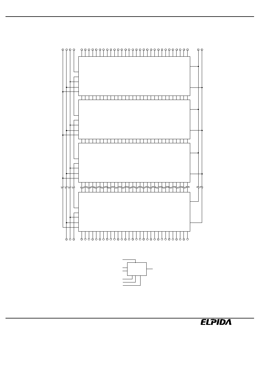
Block Diagram
LDQA 8
LDQA 7
LDQA 6
LDQA 5
LDQA 4
LDQA 3
LDQA 2
LDQA 1
LDQA 0
LCFM
LCFMN
LCTM
LCTMN
LROW 2
LROW 1
LROW 0
LCOL 4
LCOL 3
LCOL 2
LCOL 1
LCOL 0
LDQB 0
LDQB 1
LDQB 2
LDQB 3
LDQB 4
LDQB 5
LDQB 6
LDQB 7
LDQB 8
RDQA 8
RDQA 7
RDQA 6
RDQA 5
RDQA 4
RDQA 3
RDQA 2
RDQA 1
RDQA 0
RCFM
RCFMN
RCTM
RCTMN
RROW 2
RROW 1
RROW 0
RCOL 4
RCOL 3
RCOL 2
RCOL 1
RCOL 0
RDQB 0
RDQB 1
RDQB 2
RDQB 3
RDQB 4
RDQB 5
RDQB 6
RDQB 7
RDQB 8
DQA 8
DQA 7
DQA 6
DQA 5
DQA 4
DQA 3
DQA 2
DQA 1
DQA 0
CFM
CFMN
CTM
CTMN
ROW 2
ROW 1
ROW 0
COL 4
COL 3
COL 2
COL 1
COL 0
DQB 0
DQB 1
DQB 2
DQB 3
DQB 4
DQB 5
DQB 6
DQB 7
DQB 8
SIO 0
SIO 1
SCK
CMD
V
REF
SIO 0
SIO 1
SCK
CMD
V
REF
DQA 8
DQA 7
DQA 6
DQA 5
DQA 4
DQA 3
DQA 2
DQA 1
DQA 0
CFM
CFMN
CTM
CTMN
ROW 2
ROW 1
ROW 0
COL 4
COL 3
COL 2
COL 1
COL 0
DQB 0
DQB 1
DQB 2
DQB 3
DQB 4
DQB 5
DQB 6
DQB 7
DQB 8
SIO 0
SIO 1
SCK
CMD
V
REF
DQA 8
DQA 7
DQA 6
DQA 5
DQA 4
DQA 3
DQA 2
DQA 1
DQA 0
CFM
CFMN
CTM
CTMN
ROW 2
ROW 1
ROW 0
COL 4
COL 3
COL 2
COL 1
COL 0
DQB 0
DQB 1
DQB 2
DQB 3
DQB 4
DQB 5
DQB 6
DQB 7
DQB 8
SIO 0
SIO 1
SCK
CMD
V
REF
SIN
LSCK
LCMD
V
REF
SOUT
RSCK
RCMD
U1
U2
U3
U8
DQA 8
DQA 7
DQA 6
DQA 5
DQA 4
DQA 3
DQA 2
DQA 1
DQA 0
CFM
CFMN
CTM
CTMN
ROW 2
ROW 1
ROW 0
COL 4
COL 3
COL 2
COL 1
COL 0
DQB 0
DQB 1
DQB 2
DQB 3
DQB 4
DQB 5
DQB 6
DQB 7
DQB 8
V
DD
V
CMOS
SCL
SDA
A0 A1
SCL
SA0
SA1
Serial PD
A2
SA2
WP
SWP
U0
VCC
SVDD
SDA
Note: 1. Rambus Channel signals form a loop through the RIMM module, with the exception of the SIO chain.
2. See Serial Presence Detection Specification for information on the SPD device and its contents.

EBR25EC8ABFD
Data Sheet E0310E20 (Ver. 2.0)
7
Electrical Specifications
Absolute Maximum Ratings
Symbol
Parameter
min.
max.
Unit
VI,ABS
Voltage applied to any RSL or CMOS signal pad with
respect to GND
-
0.3
VDD + 0.3
V
VDD,ABS
Voltage on VDD with respect to GND
-
0.5
VDD + 1.0
V
TSTORE
Storage temperature
-
50
+100
∞C
Caution
Exposing the device to stress above those listed in Absolute Maximum Ratings could cause
permanent damage. The device is not meant to be operated under conditions outside the limits
described in the operational section of this specification Exposure to Absolute Maximum Rating
conditions for extended periods may affect device reliability.
DC Recommended Electrical Conditions
Symbol
Parameter and conditions
min.
max.
Unit
VDD
Supply voltage*
1
2.50
-
0.13
2.50 + 0.13
V
VCMOS
CMOS I/O power supply at pad
2.5V controllers
2.50
-
0.13
2.50 + 0.25
V
1.8V controllers
1.8
-
0.1
1.8 + 0.2
V
VREF
Reference voltage*
1
1.4
-
0.2
1.4 + 0.2
V
SVDD
Serial Presence Detector- positive power
supply
2.2
3.6
V
Note: See Direct RDRAM datasheet for more details.

EBR25EC8ABFD
Data Sheet E0310E20 (Ver. 2.0)
8
AC Electrical Specifications
Symbol
Parameter and Conditions
Grade
min.
typ.
max.
Unit
Z
Module Impedance of RSL signals
25.2
28.0
30.8
Module Impedance of SCK and CMD signals
23.8
28.0
32.2
TPD
Average clock delay from finger to finger of all RSL
clock nets (CTM, CTMN,CFM, and CFMN)
--
--
1.56
ns
TPD
Propagation delay variation of RSL signals with respect
to TPD
*
1, 2
-21
--
21
ps
TPD-CMOS
Propagation delay variation of SCK signal with respect
to an average clock delay
*
1
-250
--
250
ps
TPD- SCK,CMD
Propagation delay variation of CMD signal with respect
to SCK signal
-200
--
200
ps
V
/VIN
Attenuation Limit
-AEP
-AE
-AD
-8C
--
--
17.0
%
VXF/VIN
Forward crosstalk coefficient
(300ps input rise time 20% - 80%)
-AEP
-AE
-AD
-8C
--
--
4.0
%
VXB/VIN
Backward crosstalk coefficient
(300ps input rise time 20% - 80%)
-AEP
-AE
-AD
-8C
--
--
2.0
%
RDC
DC Resistance Limit
-AEP
-AE
-AD
-8C
--
--
0.8
Notes 1. TPD or Average clock delay is defined as the average delay from finger to finger of all RSL clock nets
(CTM, CTMN, CFM, and CFMN).
2. If the RIMM module meets the following specification, then it is compliant to the specification.
If the RIMM module does not meet these specifications, then the specification can be adjusted by the
"Adjusted
TPD Specification" table.
Adjusted
TPD Specification
Absolute
Symbol
Parameter and conditions
Adjusted min./max.
min.
max.
Unit
TPD
Propagation delay variation of RSL signals with
respect to TPD
+/
-
[17+(18*N*
Z0)]
*
1
-30
30
ps
Note: 1 N = Number of RDRAM devices installed on the RIMM module.
Z0 = delta Z0% = (max. Z0 - min. Z0) / (min. Z0)
(max. Z0 and min. Z0 are obtained from the loaded (high impedance) impedance coupons of all RSL
layers on the module.)

EBR25EC8ABFD
Data Sheet E0310E20 (Ver. 2.0)
9
RIMM Module Current Profile
IDD
RIMM module power conditions
*
1
Grade
max.
Unit
IDD1
One RDRAM device in Read *
2
,
balance in NAP mode
-AEP, -AE, -AD
-8C
688
548
mA
IDD2
One RDRAM device in Read *
2
,
balance in Standby mode
-AEP, -AE, -AD
-8C
1290
1010
mA
IDD3
One RDRAM device in Read *
2
,
balance in Active mode
-AEP, -AE, -AD
-8C
1570
1220
mA
IDD4
One RDRAM device in Write,
balance in NAP mode
-AEP, -AE, -AD
-8C
708
558
mA
IDD5
One RDRAM device in Write,
balance in Standby mode
-AEP, -AE, -AD
-8C
1310
1020
mA
IDD6
One RDRAM device in Write,
balance in Active mode
-AEP, -AE, -AD
-8C
1590
1230
mA
Notes: 1. Actual power will depend on individual RDRAM component specifications, memory controller and usage
patterns. Power does not include Refresh Current.
2. I/O current is a function of the % of 1's, to add I/O power for 50 % 1's for a x18 need to add 276mA for the
following: VDD = 2.5V, VTERM = 1.8V, VREF = 1.4V and VDIL = VREF
-
0.5V.
EBR25EC8ABFD
Data Sheet E0310E20 (Ver. 2.0)
10
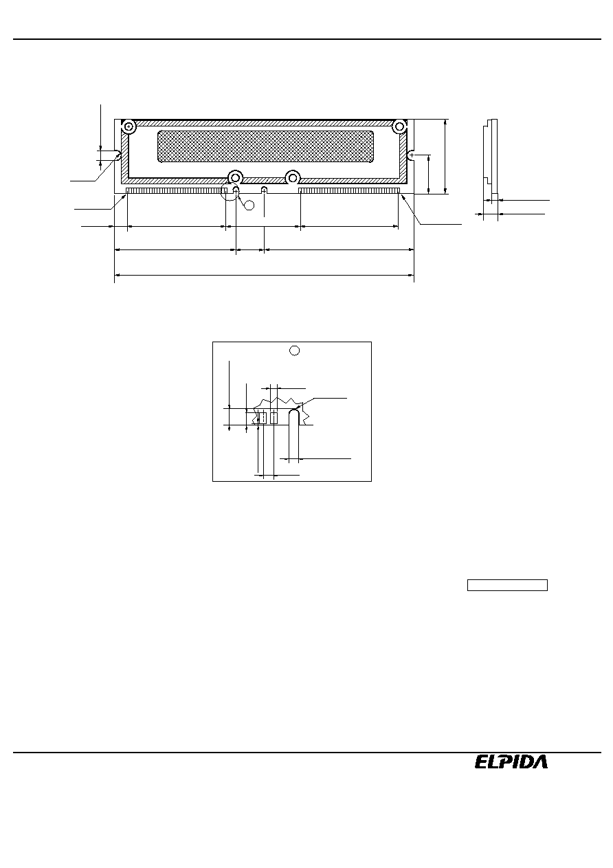
Physical Outline
Pad A1
Pad A92
ECA-TS2-0079-01
133.35
32.0
11.50
45.00
45.00
55.175
4.46 Max
1.27±0.10
17.78
4.00± 0.10
detail of A part
R1.00
2.00±0.10
0.80
3.00± 0.10
2.99
A
1.00
Unit: mm
Note: The dimensions without tolerance specification use the default tolerance of ± 0.13.
5.68
66.675
R2.00
0.30± 0.10
34.925

EBR25EC8ABFD
Data Sheet E0310E20 (Ver. 2.0)
11
CAUTION FOR HANDLING MEMORY MODULES
When handling or inserting memory modules, be sure not to touch any components on the modules, such as
the memory ICs, chip capacitors and chip resistors. It is necessary to avoid undue mechanical stress on
these components to prevent damaging them.
In particular, do not push module cover or drop the modules in order to protect from mechanical defects,
which would be electrical defects.
When re-packing memory modules, be sure the modules are not touching each other.
Modules in contact with other modules may cause excessive mechanical stress, which may damage the
modules.
MDE0202
NOTES FOR CMOS DEVICES
1
PRECAUTION AGAINST ESD FOR MOS DEVICES
Exposing the MOS devices to a strong electric field can cause destruction of the gate
oxide and ultimately degrade the MOS devices operation. Steps must be taken to stop
generation of static electricity as much as possible, and quickly dissipate it, when once
it has occurred. Environmental control must be adequate. When it is dry, humidifier
should be used. It is recommended to avoid using insulators that easily build static
electricity. MOS devices must be stored and transported in an anti-static container,
static shielding bag or conductive material. All test and measurement tools including
work bench and floor should be grounded. The operator should be grounded using
wrist strap. MOS devices must not be touched with bare hands. Similar precautions
need to be taken for PW boards with semiconductor MOS devices on it.
2
HANDLING OF UNUSED INPUT PINS FOR CMOS DEVICES
No connection for CMOS devices input pins can be a cause of malfunction. If no
connection is provided to the input pins, it is possible that an internal input level may be
generated due to noise, etc., hence causing malfunction. CMOS devices behave
differently than Bipolar or NMOS devices. Input levels of CMOS devices must be fixed
high or low by using a pull-up or pull-down circuitry. Each unused pin should be connected
to V
DD
or GND with a resistor, if it is considered to have a possibility of being an output
pin. The unused pins must be handled in accordance with the related specifications.
3
STATUS BEFORE INITIALIZATION OF MOS DEVICES
Power-on does not necessarily define initial status of MOS devices. Production process
of MOS does not define the initial operation status of the device. Immediately after the
power source is turned ON, the MOS devices with reset function have not yet been
initialized. Hence, power-on does not guarantee output pin levels, I/O settings or
contents of registers. MOS devices are not initialized until the reset signal is received.
Reset operation must be executed immediately after power-on for MOS devices having
reset function.
CME0107

EBR25EC8ABFD
Data Sheet E0310E20 (Ver. 2.0)
12
Rambus, RDRAM and the Rambus logo are registered trademarks of Rambus Inc.
Direct Rambus, Direct RDRAM, RIMM, SO-RIMM and QRSL are trademarks of Rambus Inc.
µ
BGA is a registered trademark of Tessera, Inc.
M01E0107
No part of this document may be copied or reproduced in any form or by any means without the prior
written consent of Elpida Memory, Inc.
Elpida Memory, Inc. does not assume any liability for infringement of any intellectual property rights
(including but not limited to patents, copyrights, and circuit layout licenses) of Elpida Memory, Inc. or
third parties by or arising from the use of the products or information listed in this document. No license,
express, implied or otherwise, is granted under any patents, copyrights or other intellectual property
rights of Elpida Memory, Inc. or others.
Descriptions of circuits, software and other related information in this document are provided for
illustrative purposes in semiconductor product operation and application examples. The incorporation of
these circuits, software and information in the design of the customer's equipment shall be done under
the full responsibility of the customer. Elpida Memory, Inc. assumes no responsibility for any losses
incurred by customers or third parties arising from the use of these circuits, software and information.
[Product applications]
Elpida Memory, Inc. makes every attempt to ensure that its products are of high quality and reliability.
However, users are instructed to contact Elpida Memory's sales office before using the product in
aerospace, aeronautics, nuclear power, combustion control, transportation, traffic, safety equipment,
medical equipment for life support, or other such application in which especially high quality and
reliability is demanded or where its failure or malfunction may directly threaten human life or cause risk
of bodily injury.
[Product usage]
Design your application so that the product is used within the ranges and conditions guaranteed by
Elpida Memory, Inc., including the maximum ratings, operating supply voltage range, heat radiation
characteristics, installation conditions and other related characteristics. Elpida Memory, Inc. bears no
responsibility for failure or damage when the product is used beyond the guaranteed ranges and
conditions. Even within the guaranteed ranges and conditions, consider normally foreseeable failure
rates or failure modes in semiconductor devices and employ systemic measures such as fail-safes, so
that the equipment incorporating Elpida Memory, Inc. products does not cause bodily injury, fire or other
consequential damage due to the operation of the Elpida Memory, Inc. product.
[Usage environment]
This product is not designed to be resistant to electromagnetic waves or radiation. This product must be
used in a non-condensing environment.
If you export the products or technology described in this document that are controlled by the Foreign
Exchange and Foreign Trade Law of Japan, you must follow the necessary procedures in accordance
with the relevant laws and regulations of Japan. Also, if you export products/technology controlled by
U.S. export control regulations, or another country's export control laws or regulations, you must follow
the necessary procedures in accordance with such laws or regulations.
If these products/technology are sold, leased, or transferred to a third party, or a third party is granted
license to use these products, that third party must be made aware that they are responsible for
compliance with the relevant laws and regulations.
The information in this document is subject to change without notice. Before using this document, confirm that this is the latest version.