Document Outline
- COVER
- Description
- Features
- Ordering Information
- Pin Configurations
- Pin Description
- Serial PD Matrix
- Block Diagram
- Electrical Specifications
- Absolute Maximum Ratings
- DC Operating Conditions
- DC Characteristics
- Pin Capacitance
- AC Characteristics
- Test Conditions
- Relationship Between Frequency and Minimum Latency
- Pin Functions
- Detailed Operation Part
- Physical Outline

Document No. E0227E20 (Ver. 2.0)
Date Published November 2001 (K) Japan
URL: http://www.elpida.com
Elpida Memory, Inc. 2001
C
DATA SHEET
256MB SDRAM S.O.DIMM
EBS25EC8APSA (32M words
◊
◊
◊
◊
72 bits, 1 bank)
Description
The EBS25EC8APSA is 32M words
◊
72 bits, 1 bank
Synchronous Dynamic RAM Small Outline Dual In-line
Memory Module (S.O.DIMM), mounted 9 pieces of
256M bits SDRAM (EDS2508APTA) sealed in TSOP
package. This module provides high density and large
quantities of memory in a small space without utilizing
the surface mounting technology. Decoupling
capacitors are mounted on power supply line for noise
reduction.
Features
∑
Fully compatible with 8 bytes S.O.DIMM: JEDEC
standard outline
∑
144-pin socket type small outline dual in line memory
module (S.O.DIMM)
PCB height: 38.10mm (1.5inch )
Lead pitch: 0.80mm
∑
3.3V power supply
∑
Clock frequency: 100MHz 133MHz (max.)
∑
LVTTL interface
∑
Data bus width:
◊
72 ECC
∑
Single pulsed /RAS
∑
4 Banks can operates simultaneously and
independently
∑
Burst read/write operation and burst read/single write
operation capability
∑
Programmable burst length (BL): 1, 2, 4, 8, Full page
∑
2 variations of burst sequence
Sequential
Interleave
∑
Programmable /CAS latency (CL): 2, 3
∑
Byte control by DQMB
∑
Refresh cycles: 8192 refresh cycles/64ms
∑
2 variations of refresh
Auto refresh
Self refresh
EBS25EC8APSA
Data Sheet E0227E20 (Ver. 2.0)
2
Ordering Information
Part number
Clock frequency
MHz (max.)
/CAS latency
Package
Contact pad
Mounted devices
EBS25EC8APSA-7A
EBS25EC8APSA-75 *
EBS25EC8APSA-80
133
133
100
2, 3
3
2, 3
144-pin S.O.DIMM
Gold
EDS2508APTA
EBS25EC8APSA-7AL
EBS25EC8APSA-75L*
EBS25EC8APSA-80L
133
133
100
2, 3
3
2, 3
Note: 100MHz operation at /CAS latency = 2.
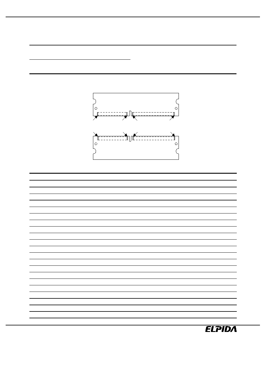
Pin Configurations
Front Side
Back Side
2pin
60pin
62pin
144pin
1pin
59pin
61pin
143pin
Front side
Back side
Pin No.
Pin name
Pin No.
Pin name
Pin No.
Pin name
Pin No.
Pin name
1
VSS
73
NC
2
VSS
74
CLK1
3
DQ0
75
VSS
4
DQ32
76
VSS
5
DQ1
77
CB4
6
DQ33
78
CB5
7
DQ2
79
CB6
8
DQ34
80
CB7
9
DQ3
81
VDD
10
DQ35
82
VDD
11
VDD
83
DQ16
12
VDD
84
DQ48
13
DQ4
85
DQ17
14
DQ36
86
DQ49
15
DQ5
87
DQ18
16
DQ37
88
DQ50
17
DQ6
89
DQ19
18
DQ38
90
DQ51
19
DQ7
91
VSS
20
DQ39
92
VSS
21
VSS
93
DQ20
22
VSS
94
DQ52
23
DQMB0
95
DQ21
24
DQMB4
96
DQ53
25
DQMB1
97
DQ22
26
DQMB5
98
DQ54
27
VDD
99
DQ23
28
VDD
100
DQ55
29
A0
101
VDD
30
A3
102
VDD
31
A1
103
A6
32
A4
104
A7
33
A2
105
A8
34
A5
106
BA0
35
VSS
107
VSS
36
VSS
108
VSS
37
DQ8
109
A9
38
DQ40
110
BA1
39
DQ9
111
A10 (AP)
40
DQ41
112
A11
41
DQ10
113
VDD
42
DQ42
114
VDD
EBS25EC8APSA
Data Sheet E0227E20 (Ver. 2.0)
3
Front side
Back side
Pin No.
Pin name
Pin No.
Pin name
Pin No.
Pin name
Pin No.
Pin name
43
DQ11
115
DQMB2
44
DQ43
116
DQMB6
45
VDD
117
DQMB3
46
VDD
118
DQMB7
47
DQ12
119
VSS
48
DQ44
120
VSS
49
DQ13
121
DQ24
50
DQ45
122
DQ56
51
DQ14
123
DQ25
52
DQ46
124
DQ57
53
DQ15
125
DQ26
54
DQ47
126
DQ58
55
VSS
127
DQ27
56
VSS
128
DQ59
57
CB0
129
VDD
58
CB1
130
VDD
59
CB2
131
DQ28
60
CB3
132
DQ60
61
CLK0
133
DQ29
62
CKE0
134
DQ61
63
VDD
135
DQ30
64
VDD
136
DQ62
65
/RAS
137
DQ31
66
/CAS
138
DQ63
67
/WE
139
VSS
68
NC
140
VSS
69
/CS0
141
SDA
70
A12
142
SCL
71
NC
143
VDD
72
NC
144
VDD
Pin Description
Pin name
Function
A0 to A12
Address input
Row address
A0 to A12
Column address A0 to A9
BA0, BA1
Bank select address
DQ0 to DQ63
Data input/output
CB0 to CB7
Check bit (Data input/output)
/CS0
Chip select input
/RAS
Row enable (/RAS) input
/CAS
Column enable (/CAS) input
/WE
Write enable input
DQMB0 to DQMB7
Byte data mask
CLK0, CLK1
Clock input
CKE0
Clock enable input
SDA
Data input/output for serial PD
SCL
Clock input for serial PD
VDD
Primary positive power supply
VSS
Ground
NC
No connection
EBS25EC8APSA
Data Sheet E0227E20 (Ver. 2.0)
4
Serial PD Matrix
Byte No. Function described
Bit7 Bit6 Bit5 Bit4 Bit3 Bit2 Bit1 Bit0 Hex value
Comments
0
Number of bytes used by module
manufacturer
1
0
0
0
0
0
0
0
80H
128 bytes
1
Total SPD memory size
0
0
0
0
1
0
0
0
08H
256 bytes
2
Memory type
0
0
0
0
0
1
0
0
04H
SDRAM
3
Number of row addresses bits
0
0
0
0
1
1
0
1
0DH
13
4
Number of column addresses bits
0
0
0
0
1
0
1
0
0AH
10
5
Number of banks
0
0
0
0
0
0
0
1
01H
1
6
Module data width
0
1
0
0
1
0
0
0
48H
72 bits
7
Module data width (continued)
0
0
0
0
0
0
0
0
00H
0
8
Module interface signal levels
0
0
0
0
0
0
0
1
01H
LVTTL
9
SDRAM cycle time at CL = 3
(highest /CAS latency)
(-7A/7AL, -75/75L)
0
1
1
1
0
1
0
1
75H
7.5ns
(-80/80L)
1
0
0
0
0
0
0
0
80H
8ns
10
SDRAM access from Clock at CL = 3
(highest /CAS latency)
(-7A/7AL, -75/75L)
0
1
0
1
0
1
0
0
54H
5.4ns
(-80/80L)
0
1
1
0
0
0
0
0
60H
6ns
11
Module configuration type
0
0
0
0
0
0
1
0
02H
ECC
12
Refresh rate/type
1
0
0
0
0
0
1
0
82H
7.8µs
13
SDRAM width
0
0
0
0
1
0
0
0
08H
◊
8
14
Error checking SDRAM width
0
0
0
0
1
0
0
0
08H
◊
8
15
SDRAM device attributes:
minimum clock delay for back-to-
back random column addresses
0
0
0
0
0
0
0
1
01H
1 CLK
16
SDRAM device attributes:
Burst lengths supported
1
0
0
0
1
1
1
1
8FH
1, 2, 4, 8, F
17
SDRAM device attributes: number of
banks on SDRAM device
0
0
0
0
0
1
0
0
04H
4
18
SDRAM device attributes:
/CAS latency
0
0
0
0
0
1
1
0
06H
2, 3
19
SDRAM device attributes:
/CS latency
0
0
0
0
0
0
0
1
01H
0
20
SDRAM device attributes:
/WE latency
0
0
0
0
0
0
0
1
01H
0
21
SDRAM device attributes
0
0
0
0
0
0
0
0
00H
22
SDRAM device attributes: General
0
0
0
0
1
1
1
0
0EH
23
SDRAM cycle time at CL = 2
(2nd highest /CAS latency)
(-7A/7AL)
0
1
1
1
0
1
0
1
75H
7.5ns
(-75/75L, -80/80L)
1
0
1
0
0
0
0
0
A0H
10ns
24
SDRAM access from Clock at CL = 2
(2nd highest /CAS latency)
(-7A/7AL)
0
1
0
1
0
1
0
0
54H
5.4ns
(-75/75L, -80/80L)
0
1
1
0
0
0
0
0
60H
6ns
25 to 26
0
0
0
0
0
0
0
0
00H
27
Minimum row precharge time
(-7A/7AL)
0
0
0
0
1
1
1
1
0FH
15ns
(-75/75L, -80/80L)
0
0
0
1
0
1
0
0
14H
20ns
EBS25EC8APSA
Data Sheet E0227E20 (Ver. 2.0)
5
Byte No. Function described
Bit7 Bit6 Bit5 Bit4 Bit3 Bit2 Bit1 Bit0 Hex value
Comments
28
Row active to row active min
(-7A/7AL, -75/75L)
0
0
0
0
1
1
1
1
0FH
15ns
(-80/80L)
0
0
0
1
0
0
0
0
10H
16ns
29
/RAS to /CAS delay min
(-7A/7AL)
0
0
0
0
1
1
1
1
0FH
15ns
(-75/75L, -80/80L)
0
0
0
1
0
1
0
0
14H
20ns
30
Minimum /RAS pulse width
(-7A/7AL, -75/75L)
0
0
1
0
1
1
0
1
2DH
45ns
(-80/80L)
0
0
1
1
0
0
0
0
30H
48ns
31
Density of each bank on module
0
1
0
0
0
0
0
0
40H
256MB
32
Address and command signal input
setup time
(-7A/7AL, -75/75L)
0
0
0
1
0
1
0
1
15H
1.5ns
(-80/80L)
0
0
1
0
0
0
0
0
20H
2ns
33
Address and command signal input
hold time
(-7A/7AL, -75/75L)
0
0
0
0
1
0
0
0
08H
0.8ns
(-80/80L)
0
0
0
1
0
0
0
0
10H
1ns
34
Data signal input setup time
(-7A/7AL, -75/75L)
0
0
0
1
0
1
0
1
15H
1.5ns
(-80/80L)
0
0
1
0
0
0
0
0
20H
2ns
35
Data signal input hold time
(-7A/7AL, -75/75L)
0
0
0
0
1
0
0
0
08H
0.8ns
(-80/80L)
0
0
0
1
0
0
0
0
10H
1ns
36 to 61
Superset information
0
0
0
0
0
0
0
0
00H
62
SPD data revision code
0
0
0
1
0
0
1
0
12H
1.2
63
Checksum for Bytes 0 to 62
(-7A/7AL)
1
0
1
0
0
0
1
1
A3H
(-75/75L)
1
1
1
0
0
1
0
0
E4H
(-80/80L)
0
0
1
0
0
1
0
1
25H
64
Manufacturer's JEDEC ID code
1
1
1
1
1
1
1
0
FEH
Elpida Memory
65 to 71
Manufacturer's JEDEC ID code
0
0
0
0
0
0
0
0
00H
72
Manufacturing location
73 to 90
Manufacturer's part number
91 to 92
Revision code
93 to 94
Manufacturing date
95 to 98
Assembly serial number
99 to 125 Manufacturer specific data
126
Reserved (Intel specification
frequency)
0
1
1
0
0
1
0
0
64H
100MHz
127
Reserved (Intel specification /CAS#
latency support)
1
1
0
0
0
1
1
1
C7H