Document Outline
- COVER
- Description
- Features
- Ordering Information
- Part Number
- Pin Configurations
- Electrical Specifications
- Absolute Maximum Ratings
- Recommended DC Operating Conditions
- DC Characteristics 1
- DC Characteristics 2
- Pin Capacitance
- AC Characteristics
- Test Conditions
- Timing Parameter Measured in Clock Cycle
- Block Diagram
- Pin Function
- Command Operation
- Command Truth Table
- CKE Truth Table
- Function Truth Table
- Command Truth Table for CKE
- Simplified State Diagram
- Operation of the DDR SDRAM
- Power-up Sequence
- Mode Register and Extended Mode Register Set
- Burst Operation
- Read/Write Operations
- Burst Stop
- Auto Precharge
- Command Intervals
- DM Control
- Timing Waveforms
- Command and Addresses Input Timing Definition
- Read Timing Definition
- Write Timing Definition
- Read Cycle
- Write Cycle
- Mode Register Set Cycle
- Read/Write Cycle
- Auto Refresh Cycle
- Self Refresh Cycle
- Package Drawing
- Recommended Soldering Conditions

Document No. E0533E50 (Ver. 5.0)
Date Published June 2005 (K) Japan
Printed in Japan
URL: http://www.elpida.com
Elpida Memory, Inc. 2004-2005
DATA SHEET
128M bits DDR SDRAM
EDD1232AABH (4M words
◊
32 bits)
Description
The EDD1232AABH is a 128M bits DDR SDRAM
organized as 1,048,576 words
◊
32 bits
◊
4 banks.
Read and write operations are performed at the cross
points of the CK and the /CK. This high-speed data
transfer is realized by the 2 bits prefetch-pipelined
architecture. Data strobe (DQS) both for read and
write are available for high speed and reliable data bus
design. By setting extended mode register, the on-chip
Delay Locked Loop (DLL) can be set enable or disable.
It is packaged in 144-ball FBGA package.
Features
∑
Power supply: VDDQ = 2.5V
±
0.2V
: VDD = 2.5V
±
0.2V
∑
Data rate: 333Mbps/266Mbps (max.)
∑
Double Data Rate architecture; two data transfers per
clock cycle
∑
Bi-directional, data strobe (DQS) is transmitted
/received with data, to be used in capturing data at
the receiver
∑
Data inputs, outputs, and DM are synchronized with
DQS
∑
4 internal banks for concurrent operation
∑
DQS is edge aligned with data for READs; center
aligned with data for WRITEs
∑
Differential clock inputs (CK and /CK)
∑
DLL aligns DQ and DQS transitions with CK
transitions
∑
Commands entered on each positive CK edge; data
and data mask referenced to both edges of DQS
∑
Data mask (DM) for write data
∑
Auto precharge option for each burst access
∑
SSTL_2 compatible I/O
∑
Programmable burst length (BL): 2, 4, 8
∑
Programmable /CAS latency (CL): 2, 2.5, 3
∑
Programmable output driver strength: half/weak
∑
Refresh cycles: 4096 refresh cycles/32ms
7.8
µ
s maximum average periodic refresh interval
∑
2 variations of refresh
Auto refresh
Self refresh
∑
FBGA package with lead free solder (Sn-Ag-Cu)
RoHS compliant
EDD1232AABH
Data Sheet E0533E50 (Ver. 5.0)
2
Ordering Information
Part number
Mask
version
Organization
(words
◊
bits)
Internal
banks
Data Rate
Mbps (max.)
JEDEC speed bin
(CL-tRCDRD-tRP)
Package
EDD1232AABH-6B-E
EDD1232AABH-7A-E
A 4M
◊
32
4
333
266
DDR333B (2.5-3-3)
DDR266A (2-3-3)
144-ball FBGA
Part Number
Elpida Memory
Density / Bank
12: 128M / 4-bank
Organization
32: x32
Power Supply, Interface
A: 2.5V, SSTL_2
Die Rev.
Package
BH: FBGA
Speed
6B: DDR333B (2.5-3-3)
7A: DDR266A (2-3-3)
Product Family
D: DDR SDRAM
Type
D: Monolithic Device
E D D 12 32 A A BH - 6B - E
Environment Code
E: Lead Free
EDD1232AABH
Data Sheet E0533E50 (Ver. 5.0)
3
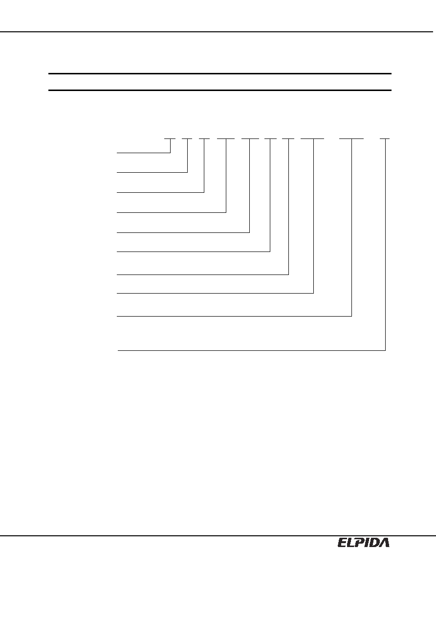
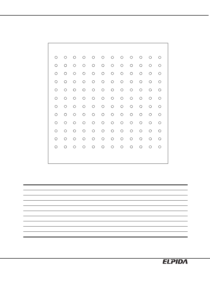
Pin Configurations
/xxx indicates active low signal.
A
B
C
D
E
F
G
H
J
K
L
M
(Top view)
144-ball FBGA
1
2
3
4
5
6
7
8
9
10
11
12
DQS0
DQ6
DQ17
DQ22
VDDQ
NC
DQ4
DQ5
VDDQ
DQ7
DQ16
DQ23
VSSQ
DM0
VSSQ
VDD
VDDQ
/WE
/CAS
VDD
VDDQ
DQ3
VDDQ
VSSQ
VSS
VSSQ
VSS
DQ2
DQ1
VDDQ
VSSQ
VSSQ
VSS
VSS
Thermal
A10
DQ0
VDD
DQ19
DQ21
DQ18
DM2
DQS2
DQ20
VDDQ
NC
VDDQ
VSSQ
VSSQ
VSS
Thermal
VSS
Thermal
VSS
Thermal
VSSQ
VSS
Thermal
VSS
Thermal
VSS
Thermal
VSS
Thermal
VSSQ
VSS
VSS
NC
/CS
BA0
A0
A1
A3
NC
NC
BA1
A2
/RAS
VDD
DQ31
VDDQ
VDD
VSS
VSS
Thermal
VDD
DQ29
DQ30 VDDQ
VSSQ
VSSQ
VSS
VSS
Thermal
RFU
DQ28
VSSQ
VSS
Thermal
VSS
Thermal
VSS
Thermal
VSS
Thermal
VSSQ
VSS
Thermal
VSS
Thermal
VSSQ
VSSQ
VSSQ
VSS
VSS
VSSQ
A4
A6
A7
A9
A11
A5
VSS
VSSQ
NC
VSSQ
VDD
VDDQ
VDD
DM3
VDDQ DQ27
DQ26
VDDQ DQ24
DQ15
NC
DQS3
DQ25
VDDQ
NC
DQ13
DM1
DQS1
VDDQ DQ11
DQ10
DQ12
DQ14
VDDQ
DQ9
DQ8
A8
(AP)
CKE
VREF
CK
RFU
/CK
MCL
NC
Pin name
Function
Pin name
Function
A0 to A11
Address inputs
CK
Clock input
BA0, BA1
Bank select address
/CK
Differential Clock input
DQ0 to DQ31
Data-input/output
CKE
Clock enable
DQS0 to DQS3
Input and output data strobe
VREF
Input reference voltage
/CS
Chip select
VDD
Power for internal circuit
/RAS
Row address strobe command
VSS
Ground for internal circuit
/CAS
Column address strobe command
VDDQ
Power for DQ circuit
/WE
Write enable
VSSQ
Ground for DQ circuit
DM0 to DM3
Input mask
MCL
Must be connected with VSS
NC
No connection
RFU*
Reserved for future use
Note: Don't connect.

EDD1232AABH
Data Sheet E0533E50 (Ver. 5.0)
4
CONTENTS
Description.....................................................................................................................................................1
Features.........................................................................................................................................................1
Ordering Information......................................................................................................................................2
Part Number ..................................................................................................................................................2
Pin Configurations .........................................................................................................................................3
Electrical Specifications.................................................................................................................................5
Block Diagram .............................................................................................................................................11
Pin Function.................................................................................................................................................12
Command Operation ...................................................................................................................................14
Simplified State Diagram .............................................................................................................................21
Operation of the DDR SDRAM ....................................................................................................................22
Timing Waveforms.......................................................................................................................................41
Package Drawing ........................................................................................................................................47
Recommended Soldering Conditions..........................................................................................................48
EDD1232AABH
Data Sheet E0533E50 (Ver. 5.0)
5
Electrical Specifications
∑
All voltages are referenced to VSS (GND).
∑
After power up, wait more than 200 µs and then, execute power on sequence and CBR (Auto) refresh before
proper device operation is achieved.
Absolute Maximum Ratings
Parameter Symbol
Rating Unit
Note
Voltage on any pin relative to VSS
VT
≠1.0 to +3.6
V
Supply voltage relative to VSS
VDD
≠1.0 to +3.6
V
Short circuit output current
IOS
50
mA
Power dissipation
PD
1.0
W
Operating ambient temperature
TA
0 to +70
∞
C
Storage temperature
Tstg
≠55 to +125
∞
C
Caution
Exposing the device to stress above those listed in Absolute Maximum Ratings could cause
permanent damage. The device is not meant to be operated under conditions outside the limits
described in the operational section of this specification. Exposure to Absolute Maximum Rating
conditions for extended periods may affect device reliability.
Recommended DC Operating Conditions (TA = 0 to +70
∞
C)
Parameter Symbol
min.
typ.
max.
Unit
Notes
Supply voltage
VDD,
VDDQ
2.3 2.5
2.7 V
1
VSS,
VSSQ
0 0
0 V
Input reference voltage
VREF
0.49
◊
VDDQ
0.50
◊
VDDQ 0.51
◊
VDDQ
V
Termination voltage
VTT
VREF ≠ 0.04
VREF
VREF + 0.04
V
Input high voltage
VIH (DC)
VREF + 0.15
--
VDDQ + 0.3
V
2
Input low voltage
VIL (DC)
≠0.3
--
VREF ≠ 0.15
V
3
Input voltage level,
CK and /CK inputs
VIN (DC)
≠0.3
--
VDDQ + 0.3
V
4
Input differential cross point
voltage, CK and /CK inputs
VIX (DC)
0.5
◊
VDDQ
-
0.2V 0.5
◊
VDDQ
0.5
◊
VDDQ + 0.2V V
Input differential voltage,
CK and /CK inputs
VID (DC)
0.36
--
VDDQ + 0.6
V
5, 6
Notes: 1. VDDQ must be lower than or equal to VDD.
2. VIH is allowed to exceed VDD up to 3.6V for the period shorter than or equal to 5ns.
3. VIL is allowed to outreach below VSS down to ≠1.0V for the period shorter than or equal to 5ns.
4. VIN (DC) specifies the allowable DC execution of each differential input.
5. VID (DC) specifies the input differential voltage required for switching.
6. VIH (CK) min assumed over VREF + 0.18V, VIL (CK) max assumed under VREF ≠ 0.18V
if measurement.